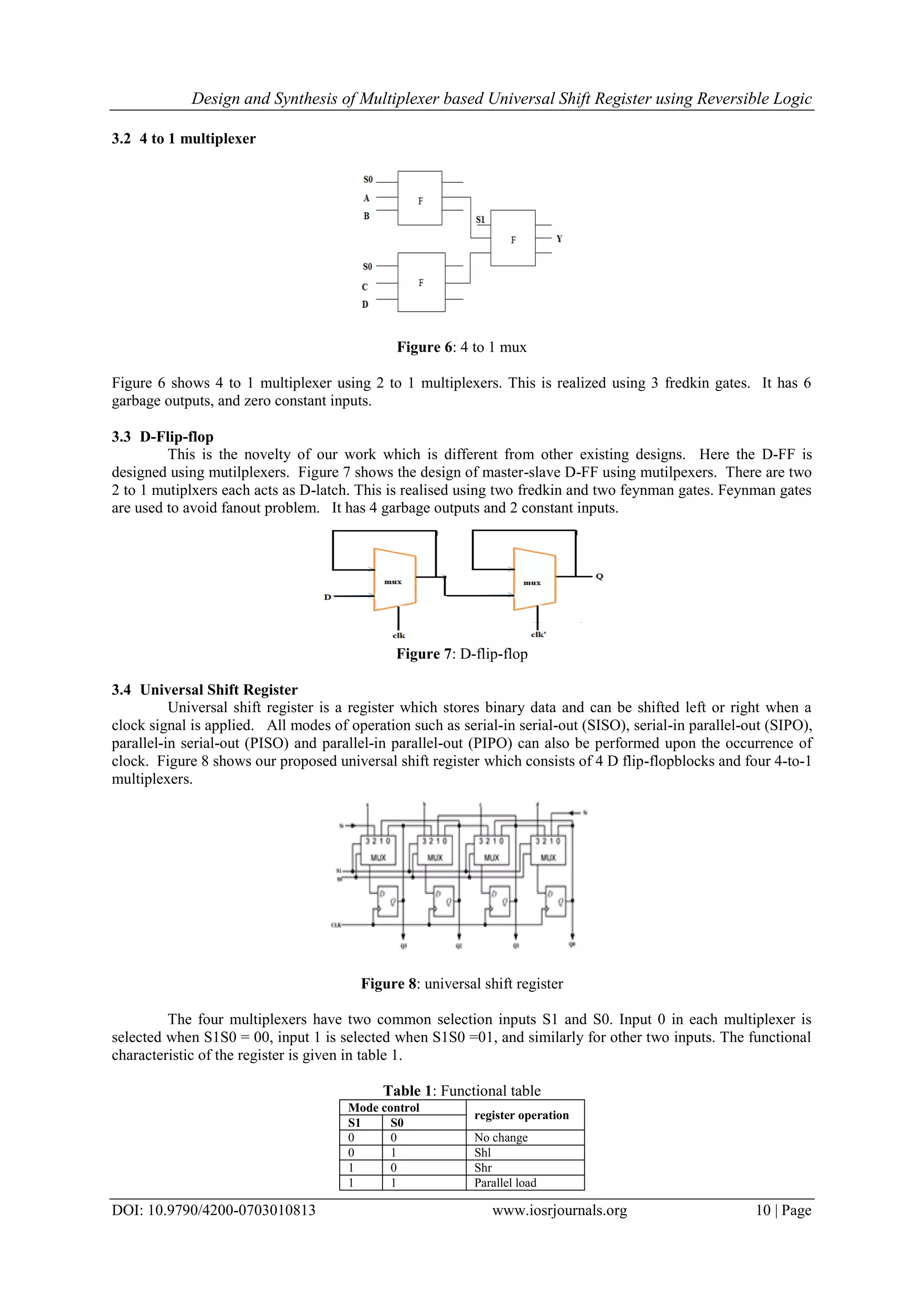
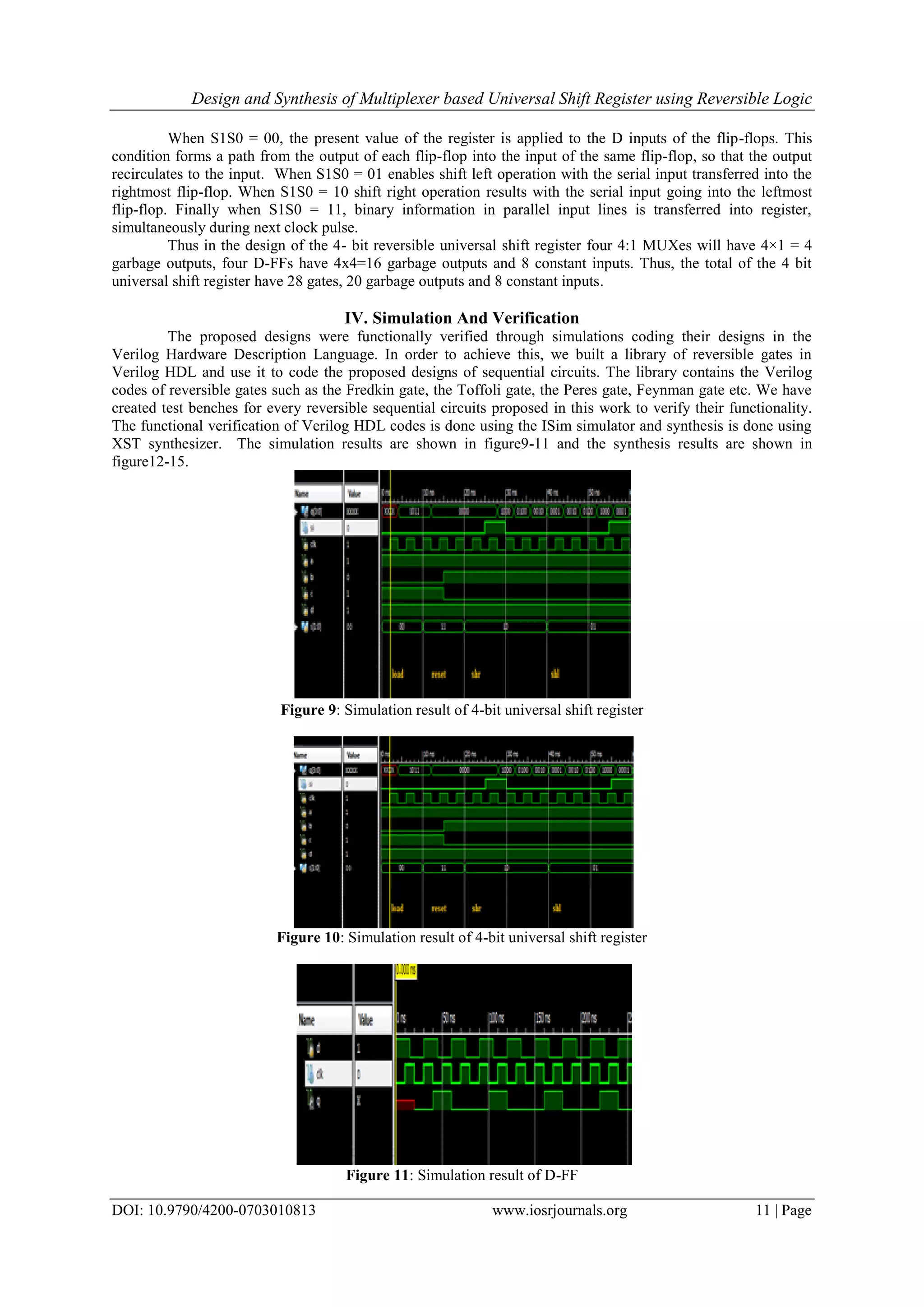
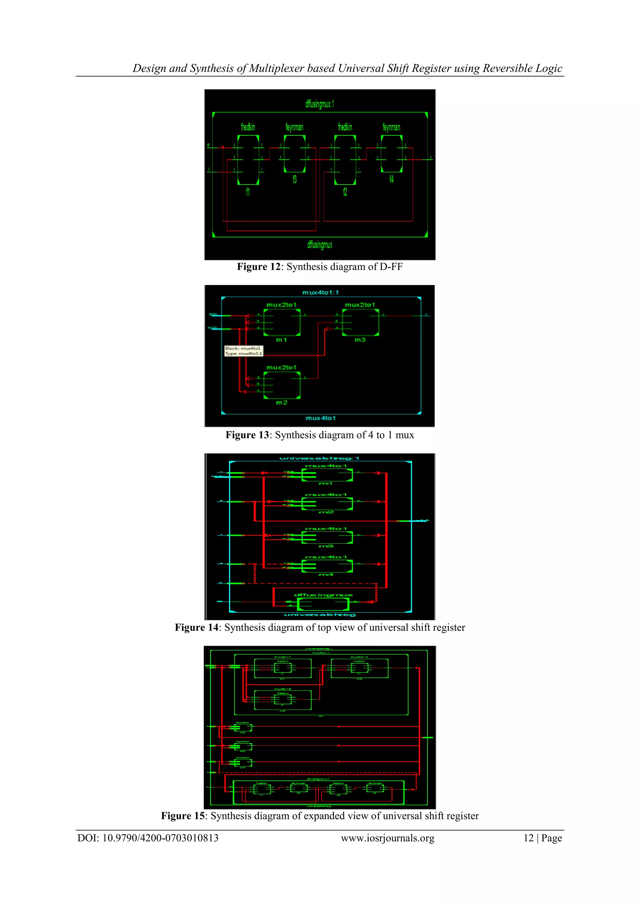
IOSR Journal of VLSI and Signal Processing (IOSR-JVSP) Volume 7, Issue 3, Ver. I (May. - Jun. 2017), PP 08-13 e-ISSN: 2319 – 4200, p-ISSN No. : 2319 – 4197 www.iosrjournals.org DOI: 10.9790/4200-0703010813 www.iosrjournals.org 8 | Page Design and Synthesis of Multiplexer based Universal Shift Register using Reversible Logic N. Srinivasa Rao1 , P.Satyanarayana2 1 Research scholar, SV University, Tirupathi, India Dept. of Telecommunication Engineering, BMS College of Engineering, Bangalore, India 2 Dept. of ECE, Annamacharya Institute of Technology and Sciences, Tirupathi, India Abstract: Reversible logic has shown wide applications in emerging technologies such as quantum computing, optical computing, and extremely low power VLSI circuits. Recently, many researchers have focused on the design and synthesis of efficient reversible logic circuits. In this work, as an example of reversible logic sequential circuits, we propose a novel reversible logic design of the Universal Shift Register. Here, we proposed a D-flip-flop whose efficiency is shown in terms of garbage output, constant input and number of reversible gates. Using this D flip-flop, efficient universal shift register is proposed. Universal shift register is a register that has both right and left shifts and parallel load capabilities. The proposed designs were functionally verified through simulations using Verilog Hardware Description Language. Keywords: Reversible Logic, Reversible Gate, Shift Register I. Introduction: In digital circuit design and synthesis, energy loss is an important consideration. Higher levels of integration and the use of new fabrication processes have dramatically reduced the heat loss over the last decades. Landauer's [1,2] principle states that logic computations generate KT log 2 Joules of heat energy for every bit of information that is lost, where Kis Boltzmann's constant and T the absolute temperature at which computation is performed. This amount may not seem to be significant, but it will become relevant for the complex circuits. Reversible design is the design that does not result in any information loss. It naturally takes care of heating generated due to the information loss. Bennett [3] showed zero energy dissipation would be possible only if the network consists of reversible gates. Thus reversibility will become an essential property in future circuit design[4]. Most traditional gates used in digital design are not reversible. For example the AND, OR and EXOR gates do not perform reversible operations. Of the commonly used gates, only the NOT gate is reversible. A set of reversible gates is needed to design reversible circuits. Several such gates have been proposed over the past decades. Among them are the controlled-not (CNOT) proposed by Feynman [5], Toffoli [6], Fredkin [7] and Peres [8]gates. Traditional design methods use, the number of gates as a complexity measure. From the point of view of reversible logic we have one more factor which is more important than the number of gates used, namely the number of garbage outputs. Since reversible design methods use reversible gates, where the number of inputs is equal tothe number of outputs, the total number of outputs of such a network will be equal to the number of inputs. The existing methods [9] use the analogy of copying information from the input of the network, therefore introducing garbage outputs -information that we do not need for the computation. In some cases garbage is unavoidable, since reversibility necessitates an equal number of outputs and inputs. This paper is organized as follows: Section 2 gives the brief introduction of the reversible logic gates and gates required for the present work. In Section 3, the designs of multiplexers and D-FFs with Fredkin gate, Reversible Universal shift register and its implementation are described. The simulation and Synthesis results are shown in section 4. Finally, Section 5 concludes with scope for further research II. Basic Reversible Gates There are a number of existing reversible gates in the literature. Some of the basic reversible logic gates are, Feynman gate: Figure 1 shows a 2x2 Feynman gate [5]. The input vector is I (A, B) and the output vector is O (P, Q) and the relation between input and output is given by P=A, Q = A⊕B.
Design and Synthesis of Multiplexer based Universal Shift Register using Reversible Logic DOI: 10.9790/4200-0703010813 www.iosrjournals.org 9 | Page Figure 1: Feynman gate Double Feynman gate (F2G): Figure 2 shows a 3x3 Double Feynman gate. The input vector is I (A, B, C) and the output vector is O (P, Q, R) and output is defined by P = A, Q = A⊕B, R = A⊕C Figure 2: Double Feynman gate Fredkin Gate: Figure 3 shows a 3*3 Fredkin gate [7]. The input vector is I (A, B, C) and the output vector is O (P, Q, R). The output is defined by P=A,Q=A′B⊕AC and R=A′C⊕AB Figure3: Fredkin gate Peres Gate:Figure 4 shows a 3*3 Peres gate [8]. The input vector is I (A, B, C) and the output vector is O (P, Q, R). The output is defined by P = A, Q = A⊕B and R=AB⊕C. Figure 4: Peres gate III. Proposed Work There are many existing designs [12] to demonstrate the working of universal shift register. In these designs, different reversible gates are used to realize various components. In this paper, authors have used only one type of reversible gate, i.e. Fredkingate for realizing multiplexer and D-FF and hence 4-bit universal shift register. 3.1 Fredkin gate used as 2 to 1 multiplexer Initially, the component 2 to 1 multiplexer [10] which is shown in Figure 5. This is demonstrated using one fredkin gate. It has two garbage outputs, and zero constant inputs. Figure 5: 2 to 1 mux
Design and Synthesis of Multiplexer based Universal Shift Register using Reversible Logic DOI: 10.9790/4200-0703010813 www.iosrjournals.org 10 | Page 3.2 4 to 1 multiplexer Figure 6: 4 to 1 mux Figure 6 shows 4 to 1 multiplexer using 2 to 1 multiplexers. This is realized using 3 fredkin gates. It has 6 garbage outputs, and zero constant inputs. 3.3 D-Flip-flop This is the novelty of our work which is different from other existing designs. Here the D-FF is designed using mutilplexers. Figure 7 shows the design of master-slave D-FF using mutilpexers. There are two 2 to 1 mutiplxers each acts as D-latch. This is realised using two fredkin and two feynman gates. Feynman gates are used to avoid fanout problem. It has 4 garbage outputs and 2 constant inputs. Figure 7: D-flip-flop 3.4 Universal Shift Register Universal shift register is a register which stores binary data and can be shifted left or right when a clock signal is applied. All modes of operation such as serial-in serial-out (SISO), serial-in parallel-out (SIPO), parallel-in serial-out (PISO) and parallel-in parallel-out (PIPO) can also be performed upon the occurrence of clock. Figure 8 shows our proposed universal shift register which consists of 4 D flip-flopblocks and four 4-to-1 multiplexers. Figure 8: universal shift register The four multiplexers have two common selection inputs S1 and S0. Input 0 in each multiplexer is selected when S1S0 = 00, input 1 is selected when S1S0 =01, and similarly for other two inputs. The functional characteristic of the register is given in table 1. Table 1: Functional table Mode control register operation S1 S0 0 0 No change 0 1 Shl 1 0 Shr 1 1 Parallel load
Design and Synthesis of Multiplexer based Universal Shift Register using Reversible Logic DOI: 10.9790/4200-0703010813 www.iosrjournals.org 11 | Page When S1S0 = 00, the present value of the register is applied to the D inputs of the flip-flops. This condition forms a path from the output of each flip-flop into the input of the same flip-flop, so that the output recirculates to the input. When S1S0 = 01 enables shift left operation with the serial input transferred into the rightmost flip-flop. When S1S0 = 10 shift right operation results with the serial input going into the leftmost flip-flop. Finally when S1S0 = 11, binary information in parallel input lines is transferred into register, simultaneously during next clock pulse. Thus in the design of the 4- bit reversible universal shift register four 4:1 MUXes will have 4×1 = 4 garbage outputs, four D-FFs have 4x4=16 garbage outputs and 8 constant inputs. Thus, the total of the 4 bit universal shift register have 28 gates, 20 garbage outputs and 8 constant inputs. IV. Simulation And Verification The proposed designs were functionally verified through simulations coding their designs in the Verilog Hardware Description Language. In order to achieve this, we built a library of reversible gates in Verilog HDL and use it to code the proposed designs of sequential circuits. The library contains the Verilog codes of reversible gates such as the Fredkin gate, the Toffoli gate, the Peres gate, Feynman gate etc. We have created test benches for every reversible sequential circuits proposed in this work to verify their functionality. The functional verification of Verilog HDL codes is done using the ISim simulator and synthesis is done using XST synthesizer. The simulation results are shown in figure9-11 and the synthesis results are shown in figure12-15. Figure 9: Simulation result of 4-bit universal shift register Figure 10: Simulation result of 4-bit universal shift register Figure 11: Simulation result of D-FF
Design and Synthesis of Multiplexer based Universal Shift Register using Reversible Logic DOI: 10.9790/4200-0703010813 www.iosrjournals.org 12 | Page Figure 12: Synthesis diagram of D-FF Figure 13: Synthesis diagram of 4 to 1 mux Figure 14: Synthesis diagram of top view of universal shift register Figure 15: Synthesis diagram of expanded view of universal shift register
Design and Synthesis of Multiplexer based Universal Shift Register using Reversible Logic DOI: 10.9790/4200-0703010813 www.iosrjournals.org 13 | Page V. Conclusion In this work, the authors have presented the novel design of reversible universal shift register. Here all the components are based on multiplexers. The present work differs from the existing approaches in the literature that have optimized the reversible sequential circuit designs in terms of number of reversible gates and garbage outputs. The reversible designs are functionally verified at the logical level by using Verilog hardware description language. The simulation and synthesis results are also presented. One of the limitations of our work is that it does not calculate the delay and quantum cost of the reversible sequential circuits. The next future step in the design of reversible sequential circuits is to investigate synthesis of reversible sequential circuits with above parameters. References [1]. R. Landauer,“Irreversibility and heat generation in the computing process”, IBMJ. Research and Development, pages: 183-191, 1961. [2]. R. W. Keyes and R. Landauer, “Minimal energy dissipation in logic”,IBM J. Research and Development, pages 152-157, March 1970. [3]. C. H. Bennett, “Logical reversibility of computation”,IBM J. Research and Development, pages: 525-532, November 1973. [4]. C. H. Bennett, “Notes on the history of reversible computation”,IBM J. Research and Development, 32(1):16-23, January 1988. [5]. R. Feynman, “Quantum Mechanical Computers”, optics News, Vol.11, pp. 11–20, 1985. [6]. T. Toffoli, “Reversible Computing,” Tech memo MIT/LCS/TM-151, MIT Lab for Comp. Sci, 1980. [7]. E. Fredkin and T. Toffoli, “Conservative logic,”Int’l J. Theoretical Physics, Vol. 21, pp.219–253, 1982. [8]. A. Peres, “Reversible Logic and Quantum Computers”, Physical review A, 32:3266- 3276, 1985. [9]. A. Mishchenko and M. Perkowski, “ Logic synthesis of reversible wave cascades”, International Workshop on Logic Synthesis, pages 197-202, June 2002. [10]. N.SrinivasaRao and P.Satyanarayana, “Realization of Logic Functions using Reversible Logic Gates”, International journal of VLSI System Design and Communication Systems”, ISSN 2322-0929 Vol.04, Issue.07, July-2016, Pages: 543-546 [11]. D.Michael Miller, Dmitri Maslov, and GergardWDueck, “A Transformation based Algorithm for reversible Logic Synthesis”, Annual ACM IEEE Design Automation Conference Proceedings of the 40th annual design automation conference, Anaheim CA, USA Pages: 318-327 [12]. H. Thapliyal and A. P. Vinod, “Design of reversible sequential elements with feasibility of transistor implementation” In Proc. the 2007 IEEE Intl. Symp. On Cir.and Sys., pages 625–628, New Orleans, USA, May 2007. [13]. AshisKumerBiswas, Lafifa Jamal, M. A. Mottalib1, Hafiz Md. HasanBabu.” Design of a Reversible Parallel Loading Shift Register” .Dhaka Univ. J.Eng& Tech. vol 1(2) 1-5, 2011. [14]. D. Krishnaveni, M. GeethaPriya, “A Novel Design of Reversible Universal Shift Register with Reduced Delay and Quantum Cost”, Journal of Computing, Volume 4, Issue 2, February 2012, ISSN 2151-9617. [15]. Md. Selim Al Mamun, Indrani Mandal, Md. Hasanuzzaman,” Design of Universal Shift Register Using Reversible Logic”, International Journal of Engineering and Technology Volume 2 No. 9, September, 2012 ISSN: 2049-3444, 2012

Design and Synthesis of Multiplexer based Universal Shift Register using Reversible Logic

  • 1.
    IOSR Journal ofVLSI and Signal Processing (IOSR-JVSP) Volume 7, Issue 3, Ver. I (May. - Jun. 2017), PP 08-13 e-ISSN: 2319 – 4200, p-ISSN No. : 2319 – 4197 www.iosrjournals.org DOI: 10.9790/4200-0703010813 www.iosrjournals.org 8 | Page Design and Synthesis of Multiplexer based Universal Shift Register using Reversible Logic N. Srinivasa Rao1 , P.Satyanarayana2 1 Research scholar, SV University, Tirupathi, India Dept. of Telecommunication Engineering, BMS College of Engineering, Bangalore, India 2 Dept. of ECE, Annamacharya Institute of Technology and Sciences, Tirupathi, India Abstract: Reversible logic has shown wide applications in emerging technologies such as quantum computing, optical computing, and extremely low power VLSI circuits. Recently, many researchers have focused on the design and synthesis of efficient reversible logic circuits. In this work, as an example of reversible logic sequential circuits, we propose a novel reversible logic design of the Universal Shift Register. Here, we proposed a D-flip-flop whose efficiency is shown in terms of garbage output, constant input and number of reversible gates. Using this D flip-flop, efficient universal shift register is proposed. Universal shift register is a register that has both right and left shifts and parallel load capabilities. The proposed designs were functionally verified through simulations using Verilog Hardware Description Language. Keywords: Reversible Logic, Reversible Gate, Shift Register I. Introduction: In digital circuit design and synthesis, energy loss is an important consideration. Higher levels of integration and the use of new fabrication processes have dramatically reduced the heat loss over the last decades. Landauer's [1,2] principle states that logic computations generate KT log 2 Joules of heat energy for every bit of information that is lost, where Kis Boltzmann's constant and T the absolute temperature at which computation is performed. This amount may not seem to be significant, but it will become relevant for the complex circuits. Reversible design is the design that does not result in any information loss. It naturally takes care of heating generated due to the information loss. Bennett [3] showed zero energy dissipation would be possible only if the network consists of reversible gates. Thus reversibility will become an essential property in future circuit design[4]. Most traditional gates used in digital design are not reversible. For example the AND, OR and EXOR gates do not perform reversible operations. Of the commonly used gates, only the NOT gate is reversible. A set of reversible gates is needed to design reversible circuits. Several such gates have been proposed over the past decades. Among them are the controlled-not (CNOT) proposed by Feynman [5], Toffoli [6], Fredkin [7] and Peres [8]gates. Traditional design methods use, the number of gates as a complexity measure. From the point of view of reversible logic we have one more factor which is more important than the number of gates used, namely the number of garbage outputs. Since reversible design methods use reversible gates, where the number of inputs is equal tothe number of outputs, the total number of outputs of such a network will be equal to the number of inputs. The existing methods [9] use the analogy of copying information from the input of the network, therefore introducing garbage outputs -information that we do not need for the computation. In some cases garbage is unavoidable, since reversibility necessitates an equal number of outputs and inputs. This paper is organized as follows: Section 2 gives the brief introduction of the reversible logic gates and gates required for the present work. In Section 3, the designs of multiplexers and D-FFs with Fredkin gate, Reversible Universal shift register and its implementation are described. The simulation and Synthesis results are shown in section 4. Finally, Section 5 concludes with scope for further research II. Basic Reversible Gates There are a number of existing reversible gates in the literature. Some of the basic reversible logic gates are, Feynman gate: Figure 1 shows a 2x2 Feynman gate [5]. The input vector is I (A, B) and the output vector is O (P, Q) and the relation between input and output is given by P=A, Q = A⊕B.
  • 2.
    Design and Synthesisof Multiplexer based Universal Shift Register using Reversible Logic DOI: 10.9790/4200-0703010813 www.iosrjournals.org 9 | Page Figure 1: Feynman gate Double Feynman gate (F2G): Figure 2 shows a 3x3 Double Feynman gate. The input vector is I (A, B, C) and the output vector is O (P, Q, R) and output is defined by P = A, Q = A⊕B, R = A⊕C Figure 2: Double Feynman gate Fredkin Gate: Figure 3 shows a 3*3 Fredkin gate [7]. The input vector is I (A, B, C) and the output vector is O (P, Q, R). The output is defined by P=A,Q=A′B⊕AC and R=A′C⊕AB Figure3: Fredkin gate Peres Gate:Figure 4 shows a 3*3 Peres gate [8]. The input vector is I (A, B, C) and the output vector is O (P, Q, R). The output is defined by P = A, Q = A⊕B and R=AB⊕C. Figure 4: Peres gate III. Proposed Work There are many existing designs [12] to demonstrate the working of universal shift register. In these designs, different reversible gates are used to realize various components. In this paper, authors have used only one type of reversible gate, i.e. Fredkingate for realizing multiplexer and D-FF and hence 4-bit universal shift register. 3.1 Fredkin gate used as 2 to 1 multiplexer Initially, the component 2 to 1 multiplexer [10] which is shown in Figure 5. This is demonstrated using one fredkin gate. It has two garbage outputs, and zero constant inputs. Figure 5: 2 to 1 mux
  • 3.
    Design and Synthesisof Multiplexer based Universal Shift Register using Reversible Logic DOI: 10.9790/4200-0703010813 www.iosrjournals.org 10 | Page 3.2 4 to 1 multiplexer Figure 6: 4 to 1 mux Figure 6 shows 4 to 1 multiplexer using 2 to 1 multiplexers. This is realized using 3 fredkin gates. It has 6 garbage outputs, and zero constant inputs. 3.3 D-Flip-flop This is the novelty of our work which is different from other existing designs. Here the D-FF is designed using mutilplexers. Figure 7 shows the design of master-slave D-FF using mutilpexers. There are two 2 to 1 mutiplxers each acts as D-latch. This is realised using two fredkin and two feynman gates. Feynman gates are used to avoid fanout problem. It has 4 garbage outputs and 2 constant inputs. Figure 7: D-flip-flop 3.4 Universal Shift Register Universal shift register is a register which stores binary data and can be shifted left or right when a clock signal is applied. All modes of operation such as serial-in serial-out (SISO), serial-in parallel-out (SIPO), parallel-in serial-out (PISO) and parallel-in parallel-out (PIPO) can also be performed upon the occurrence of clock. Figure 8 shows our proposed universal shift register which consists of 4 D flip-flopblocks and four 4-to-1 multiplexers. Figure 8: universal shift register The four multiplexers have two common selection inputs S1 and S0. Input 0 in each multiplexer is selected when S1S0 = 00, input 1 is selected when S1S0 =01, and similarly for other two inputs. The functional characteristic of the register is given in table 1. Table 1: Functional table Mode control register operation S1 S0 0 0 No change 0 1 Shl 1 0 Shr 1 1 Parallel load
  • 4.
    Design and Synthesisof Multiplexer based Universal Shift Register using Reversible Logic DOI: 10.9790/4200-0703010813 www.iosrjournals.org 11 | Page When S1S0 = 00, the present value of the register is applied to the D inputs of the flip-flops. This condition forms a path from the output of each flip-flop into the input of the same flip-flop, so that the output recirculates to the input. When S1S0 = 01 enables shift left operation with the serial input transferred into the rightmost flip-flop. When S1S0 = 10 shift right operation results with the serial input going into the leftmost flip-flop. Finally when S1S0 = 11, binary information in parallel input lines is transferred into register, simultaneously during next clock pulse. Thus in the design of the 4- bit reversible universal shift register four 4:1 MUXes will have 4×1 = 4 garbage outputs, four D-FFs have 4x4=16 garbage outputs and 8 constant inputs. Thus, the total of the 4 bit universal shift register have 28 gates, 20 garbage outputs and 8 constant inputs. IV. Simulation And Verification The proposed designs were functionally verified through simulations coding their designs in the Verilog Hardware Description Language. In order to achieve this, we built a library of reversible gates in Verilog HDL and use it to code the proposed designs of sequential circuits. The library contains the Verilog codes of reversible gates such as the Fredkin gate, the Toffoli gate, the Peres gate, Feynman gate etc. We have created test benches for every reversible sequential circuits proposed in this work to verify their functionality. The functional verification of Verilog HDL codes is done using the ISim simulator and synthesis is done using XST synthesizer. The simulation results are shown in figure9-11 and the synthesis results are shown in figure12-15. Figure 9: Simulation result of 4-bit universal shift register Figure 10: Simulation result of 4-bit universal shift register Figure 11: Simulation result of D-FF
  • 5.
    Design and Synthesisof Multiplexer based Universal Shift Register using Reversible Logic DOI: 10.9790/4200-0703010813 www.iosrjournals.org 12 | Page Figure 12: Synthesis diagram of D-FF Figure 13: Synthesis diagram of 4 to 1 mux Figure 14: Synthesis diagram of top view of universal shift register Figure 15: Synthesis diagram of expanded view of universal shift register
  • 6.
    Design and Synthesisof Multiplexer based Universal Shift Register using Reversible Logic DOI: 10.9790/4200-0703010813 www.iosrjournals.org 13 | Page V. Conclusion In this work, the authors have presented the novel design of reversible universal shift register. Here all the components are based on multiplexers. The present work differs from the existing approaches in the literature that have optimized the reversible sequential circuit designs in terms of number of reversible gates and garbage outputs. The reversible designs are functionally verified at the logical level by using Verilog hardware description language. The simulation and synthesis results are also presented. One of the limitations of our work is that it does not calculate the delay and quantum cost of the reversible sequential circuits. The next future step in the design of reversible sequential circuits is to investigate synthesis of reversible sequential circuits with above parameters. References [1]. R. Landauer,“Irreversibility and heat generation in the computing process”, IBMJ. Research and Development, pages: 183-191, 1961. [2]. R. W. Keyes and R. Landauer, “Minimal energy dissipation in logic”,IBM J. Research and Development, pages 152-157, March 1970. [3]. C. H. Bennett, “Logical reversibility of computation”,IBM J. Research and Development, pages: 525-532, November 1973. [4]. C. H. Bennett, “Notes on the history of reversible computation”,IBM J. Research and Development, 32(1):16-23, January 1988. [5]. R. Feynman, “Quantum Mechanical Computers”, optics News, Vol.11, pp. 11–20, 1985. [6]. T. Toffoli, “Reversible Computing,” Tech memo MIT/LCS/TM-151, MIT Lab for Comp. Sci, 1980. [7]. E. Fredkin and T. Toffoli, “Conservative logic,”Int’l J. Theoretical Physics, Vol. 21, pp.219–253, 1982. [8]. A. Peres, “Reversible Logic and Quantum Computers”, Physical review A, 32:3266- 3276, 1985. [9]. A. Mishchenko and M. Perkowski, “ Logic synthesis of reversible wave cascades”, International Workshop on Logic Synthesis, pages 197-202, June 2002. [10]. N.SrinivasaRao and P.Satyanarayana, “Realization of Logic Functions using Reversible Logic Gates”, International journal of VLSI System Design and Communication Systems”, ISSN 2322-0929 Vol.04, Issue.07, July-2016, Pages: 543-546 [11]. D.Michael Miller, Dmitri Maslov, and GergardWDueck, “A Transformation based Algorithm for reversible Logic Synthesis”, Annual ACM IEEE Design Automation Conference Proceedings of the 40th annual design automation conference, Anaheim CA, USA Pages: 318-327 [12]. H. Thapliyal and A. P. Vinod, “Design of reversible sequential elements with feasibility of transistor implementation” In Proc. the 2007 IEEE Intl. Symp. On Cir.and Sys., pages 625–628, New Orleans, USA, May 2007. [13]. AshisKumerBiswas, Lafifa Jamal, M. A. Mottalib1, Hafiz Md. HasanBabu.” Design of a Reversible Parallel Loading Shift Register” .Dhaka Univ. J.Eng& Tech. vol 1(2) 1-5, 2011. [14]. D. Krishnaveni, M. GeethaPriya, “A Novel Design of Reversible Universal Shift Register with Reduced Delay and Quantum Cost”, Journal of Computing, Volume 4, Issue 2, February 2012, ISSN 2151-9617. [15]. Md. Selim Al Mamun, Indrani Mandal, Md. Hasanuzzaman,” Design of Universal Shift Register Using Reversible Logic”, International Journal of Engineering and Technology Volume 2 No. 9, September, 2012 ISSN: 2049-3444, 2012