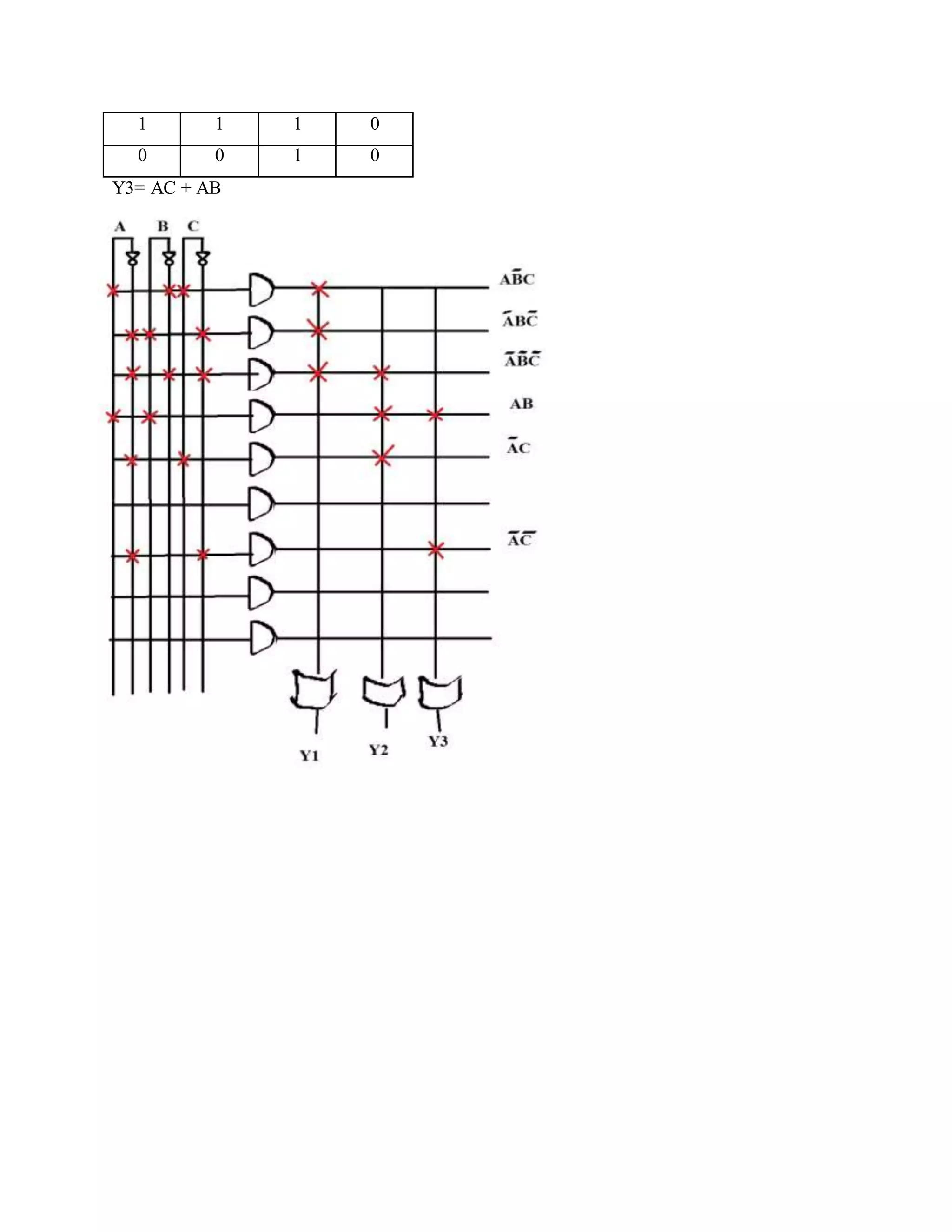
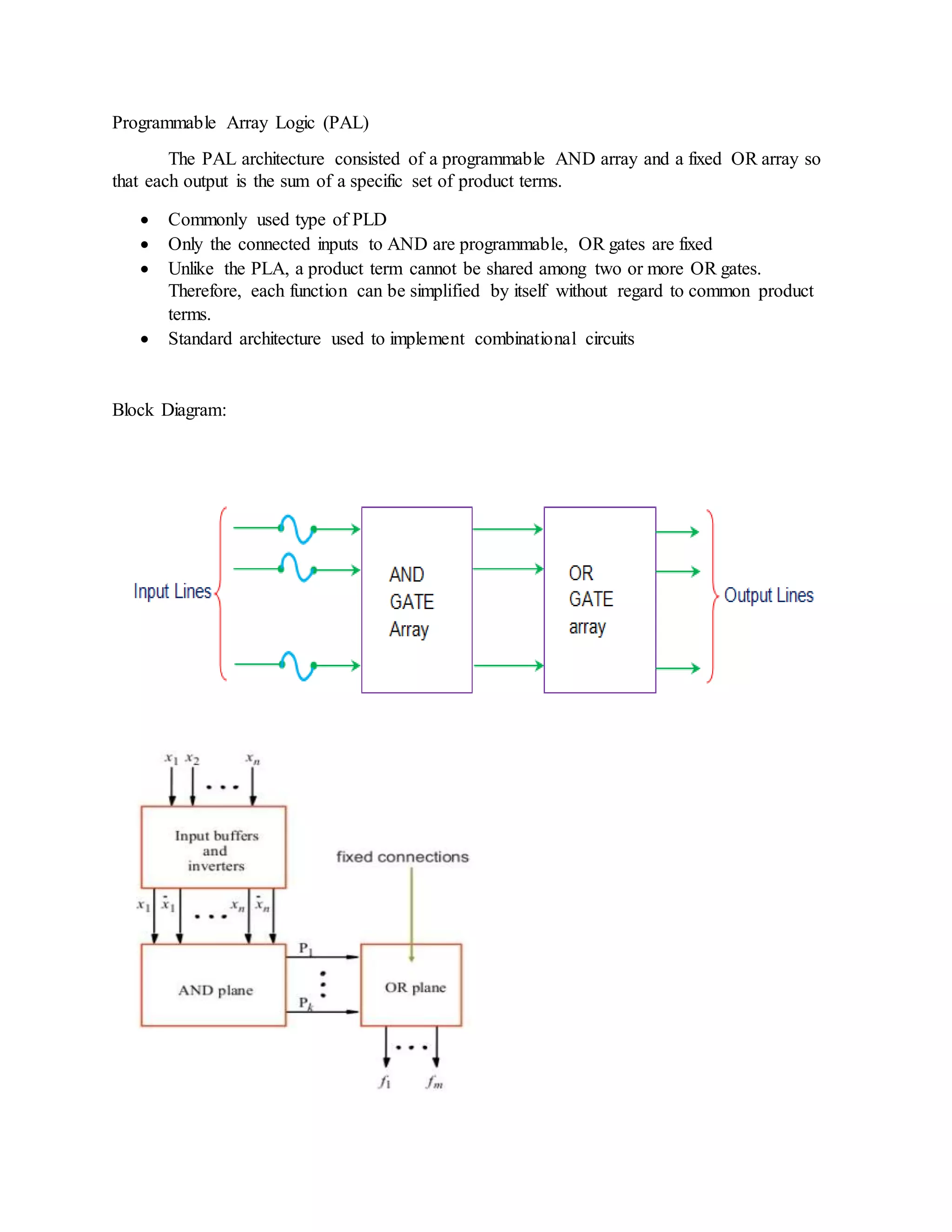
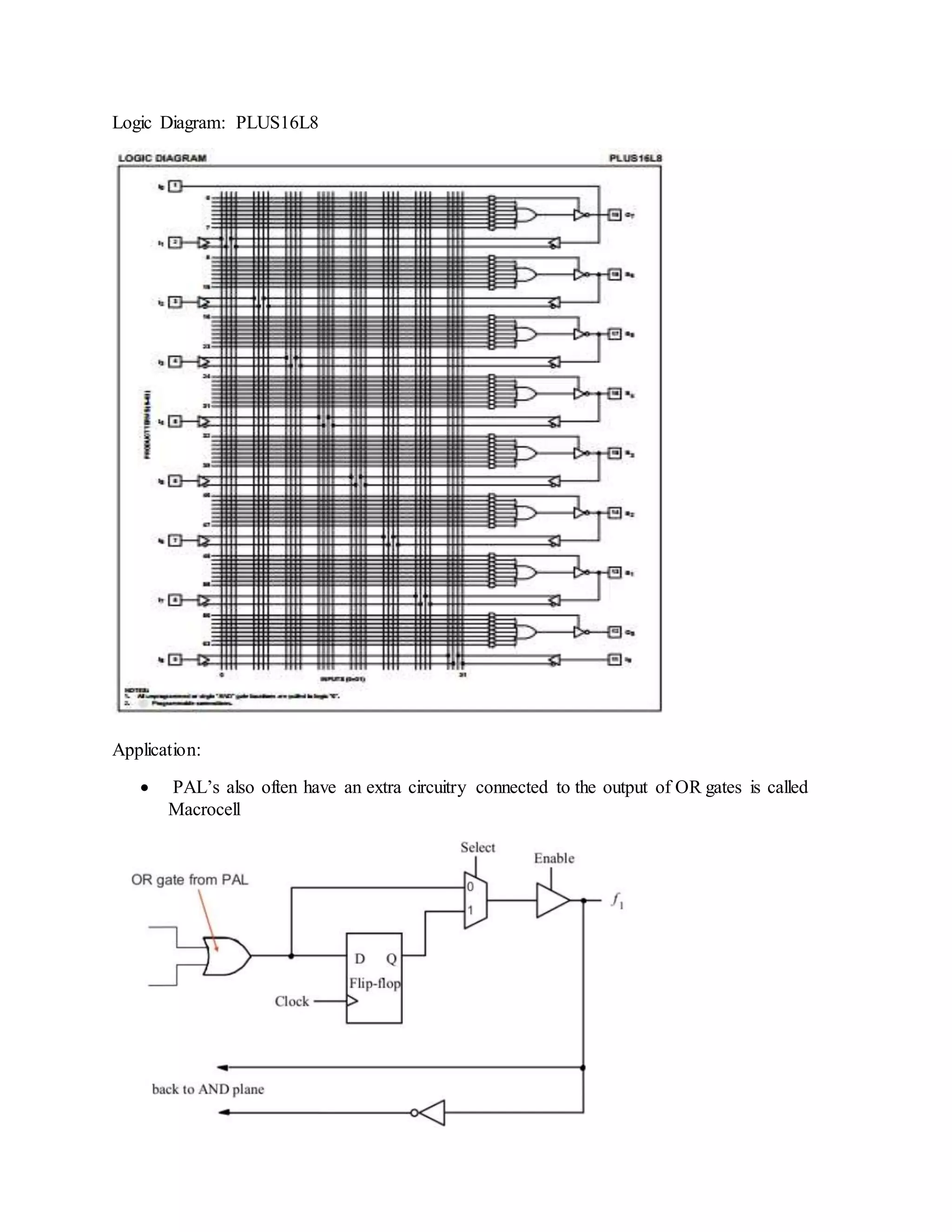
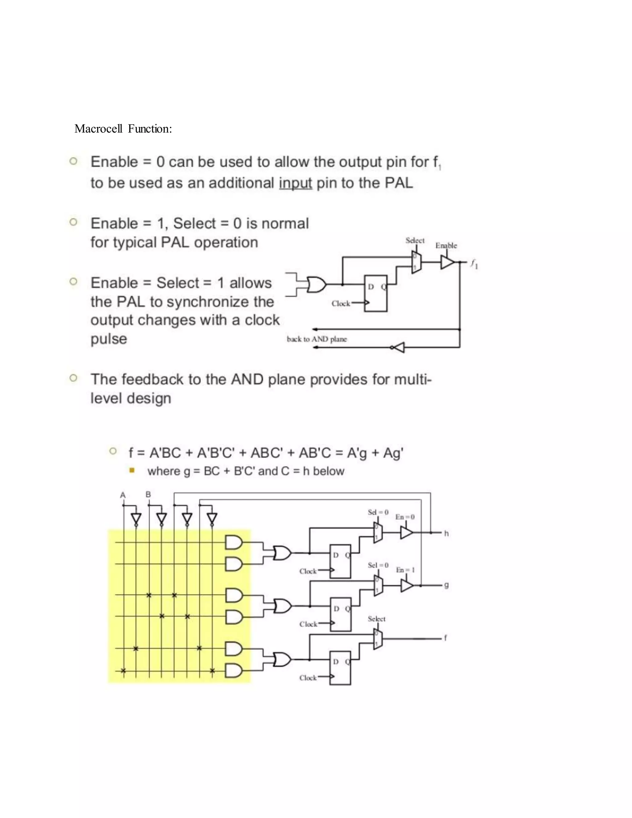
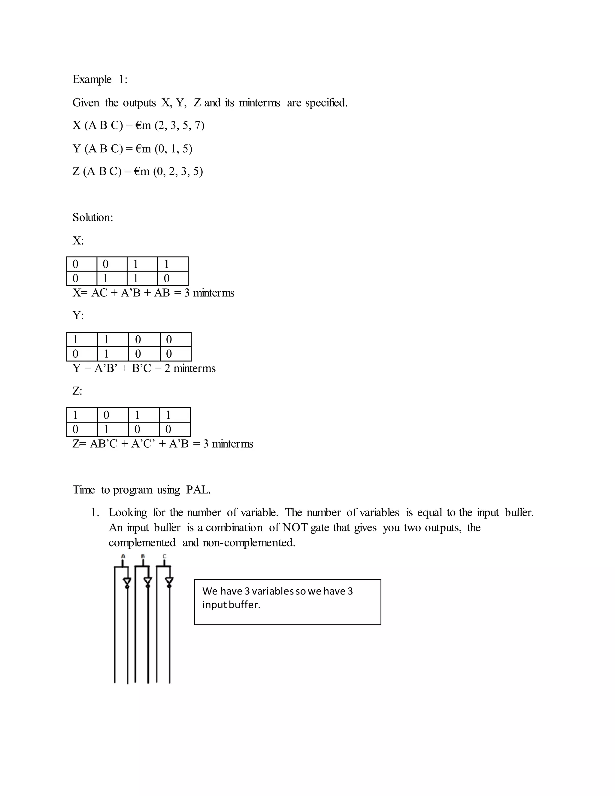
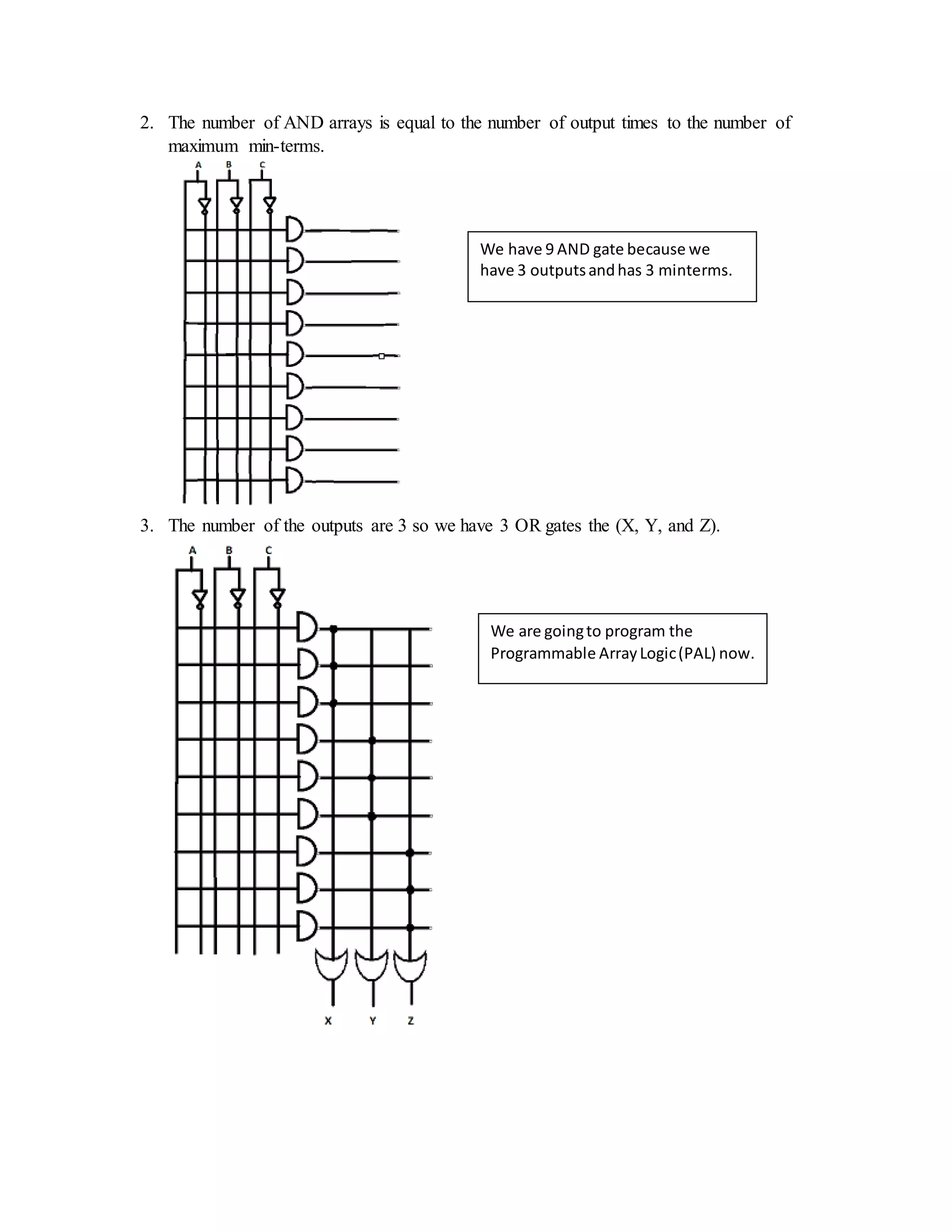
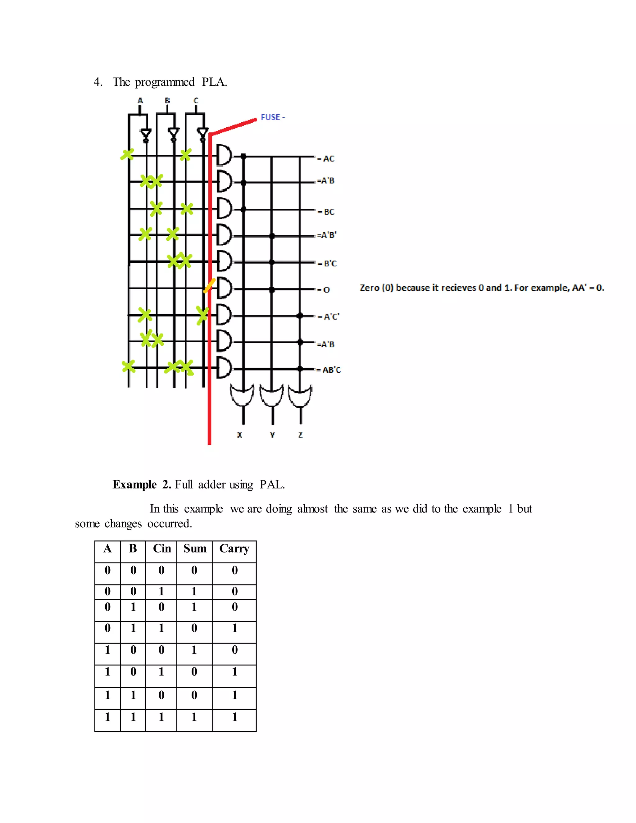
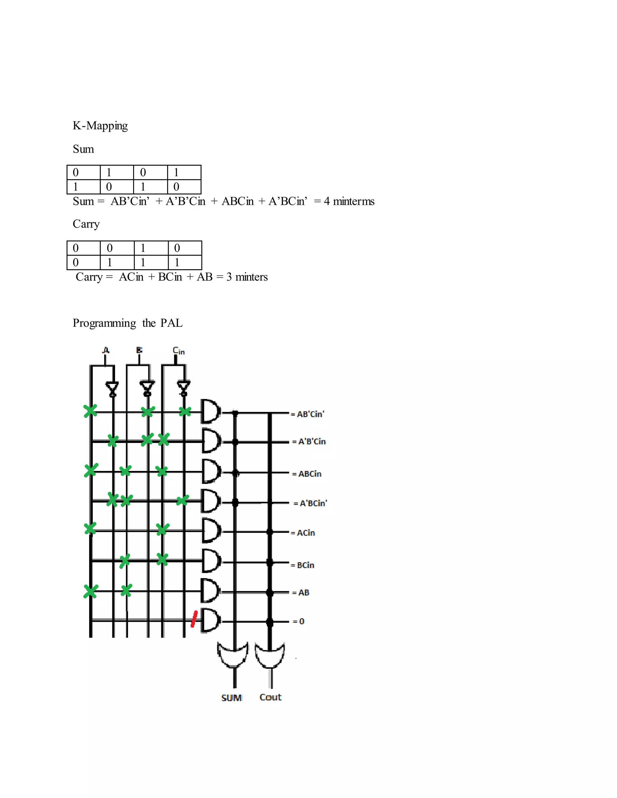
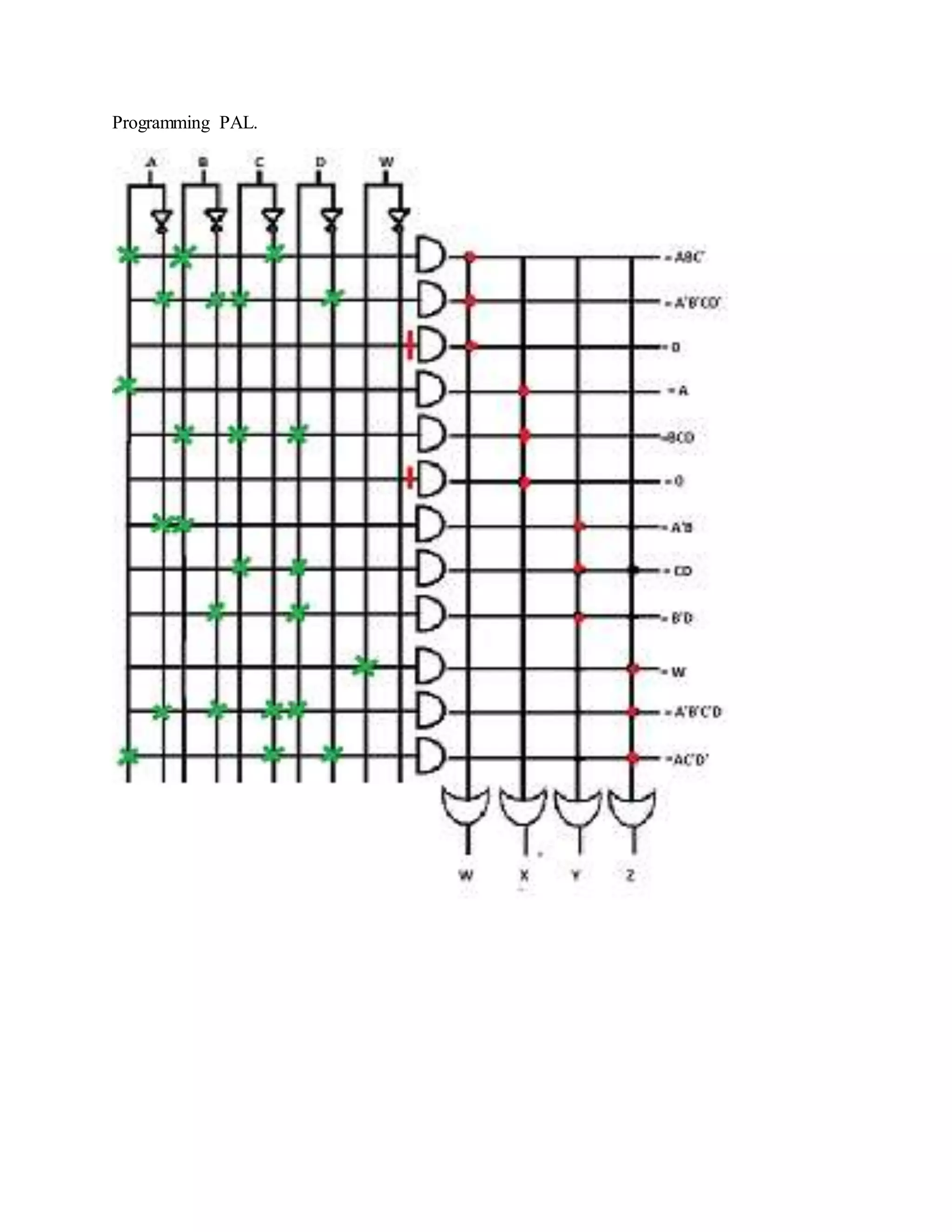
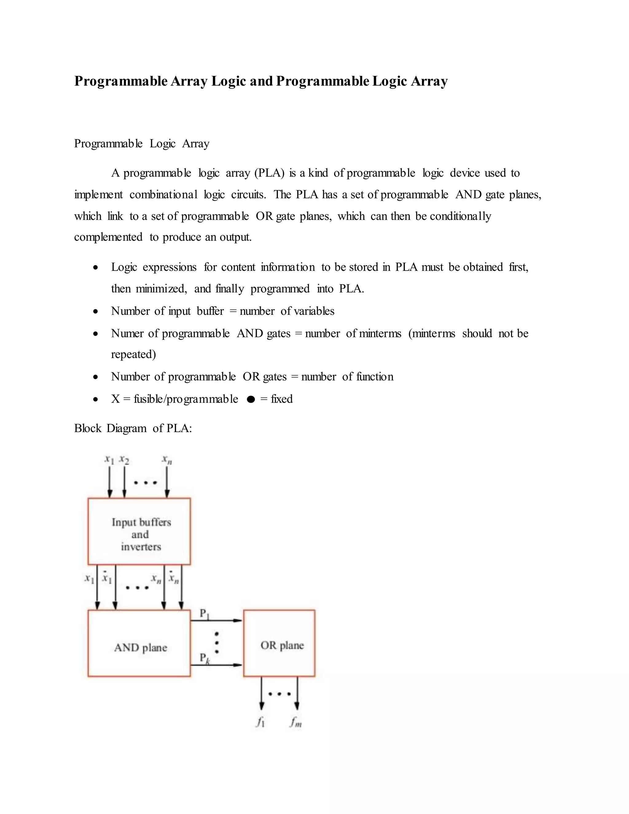
The document discusses programmable logic arrays (PLAs) and programmable array logic (PALs). PLAs have programmable AND gates that feed into programmable OR gates, allowing implementation of combinational logic circuits. PALs similarly have a programmable AND array but fixed OR gates, so each output depends on a specific set of product terms. Both PLAs and PALs can implement state machines and digital circuits through programming. Examples show mapping logic functions to the architectures and programming the resulting AND-OR configurations.
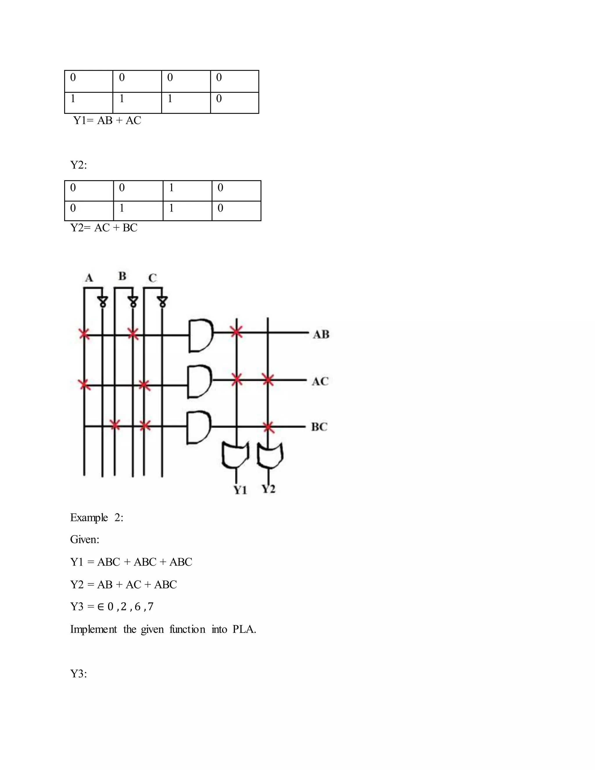
![Application: One application of a PLA is to implement the control over a datapath. It defines various states in an instruction set, and produces the next state (by conditional branching). [e.g. if the machine is in state 2, and will go to state 4 if the instruction contains an immediate field; then the PLA should define the actions of the control in state 2, will set the next state to be 4 if the instruction contains an immediate field, and will define the actions of the control in state 4]. Programmable logic arrays should correspond to a state diagram for the system. Note that the use of the word "programmable" does not indicate that all PLAs are field- programmable; in fact many are mask-programmed during manufacture in the same manner as a mask ROM. This is particularly true of PLAs that are embedded in more complex and numerous integrated circuits such as microprocessors. PLAs that can be programmed after manufacture are called FPGA (Field-programmable gate array), or less frequently FPLA (Field- programmable logic array).. The Commodore 64 home computer released in 1982 used a "906114-01 PLA" to handle system signals. Example 1: Given the truth table, design the combinational circuit using PLA. A B C Y1 Y2 0 0 0 0 0 0 0 1 0 0 0 1 0 0 0 0 1 1 0 1 1 0 0 1 0 1 0 1 1 1 1 1 0 0 0 1 1 1 1 1 Solution: Y1:](https://image.slidesharecdn.com/programmable-array-logic-and-programmable-logic-array-180305041327/75/Programmable-array-logic-and-programmable-logic-array-2-2048.jpg)