Download to read offline

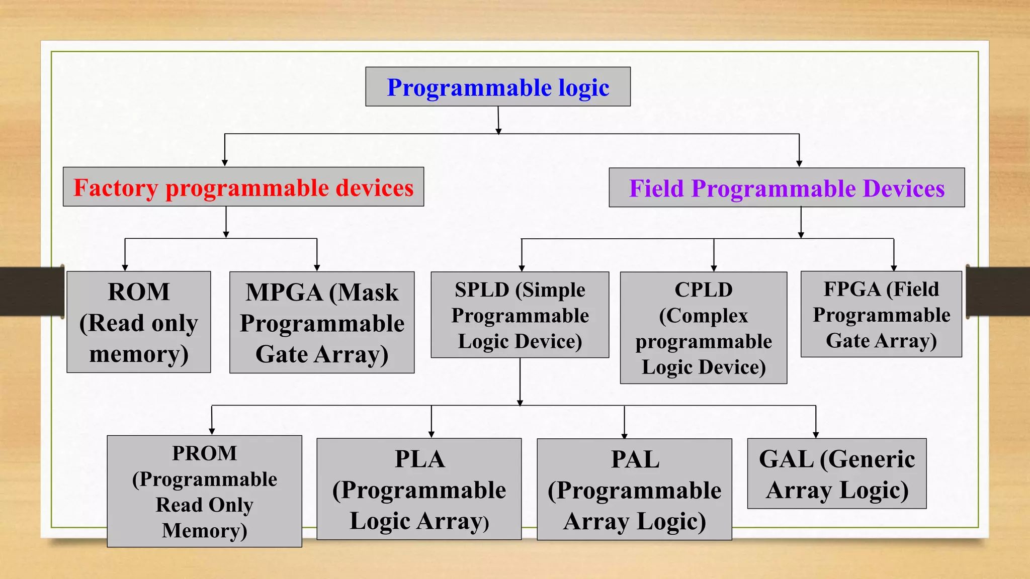
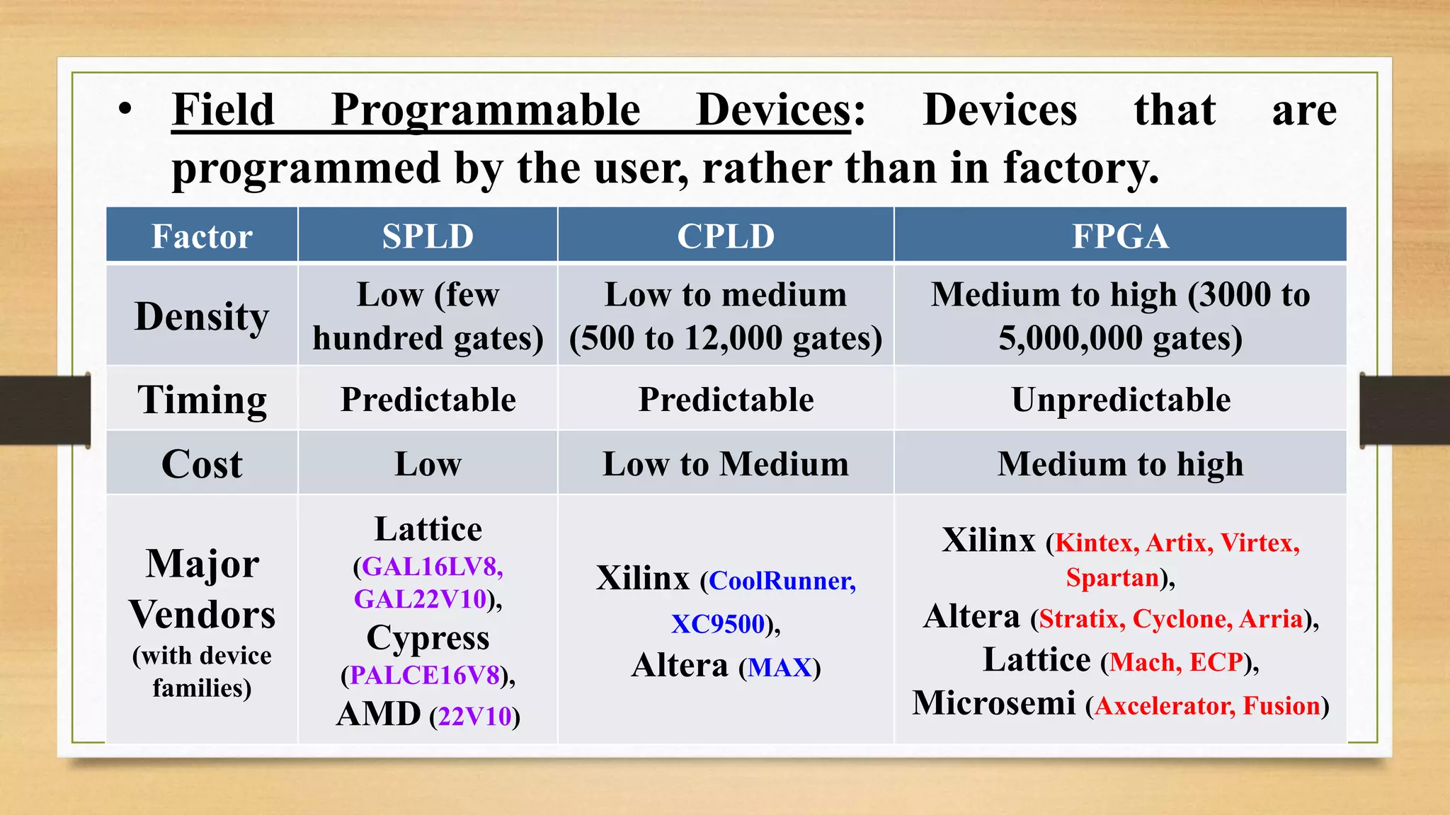
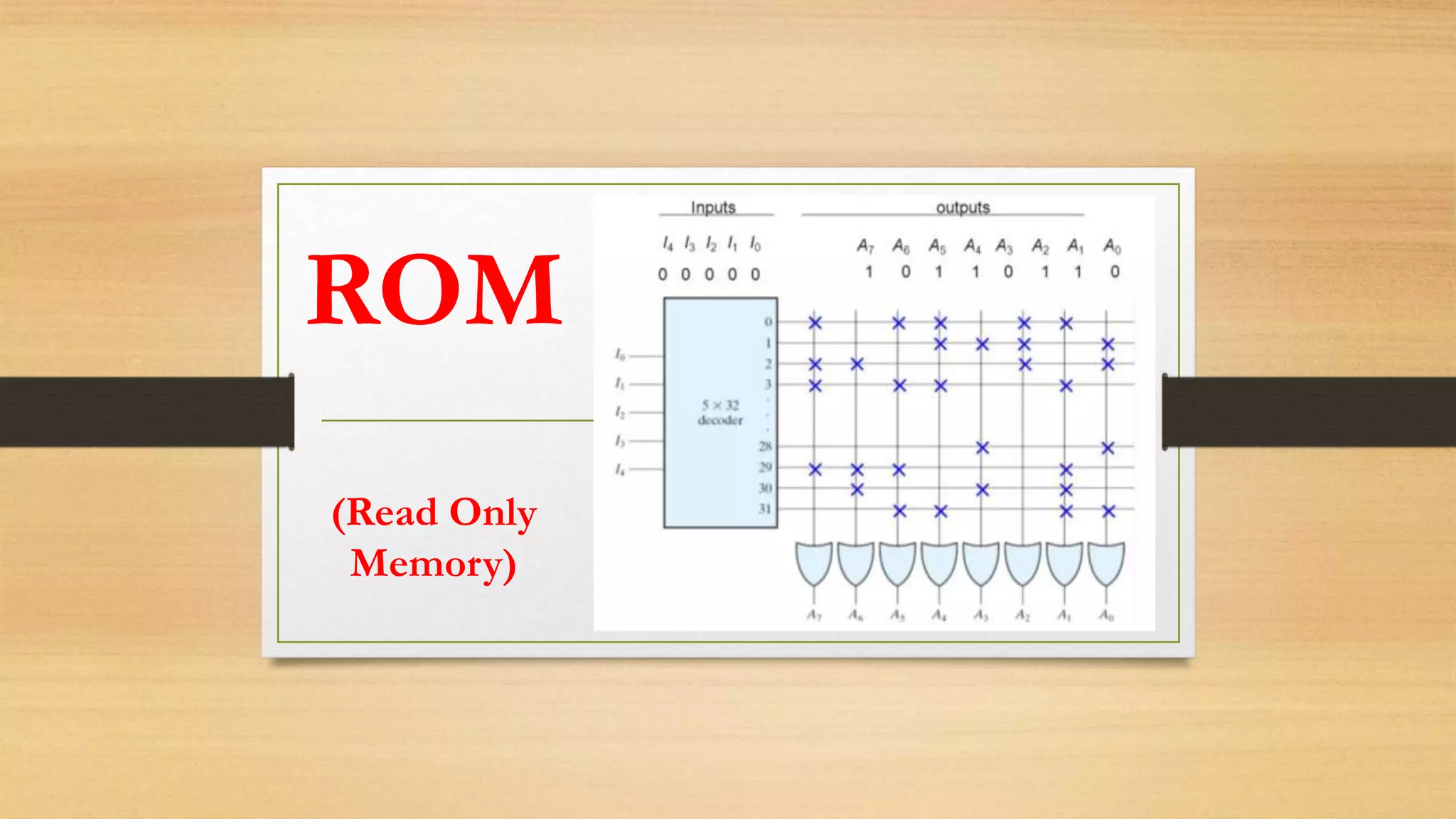
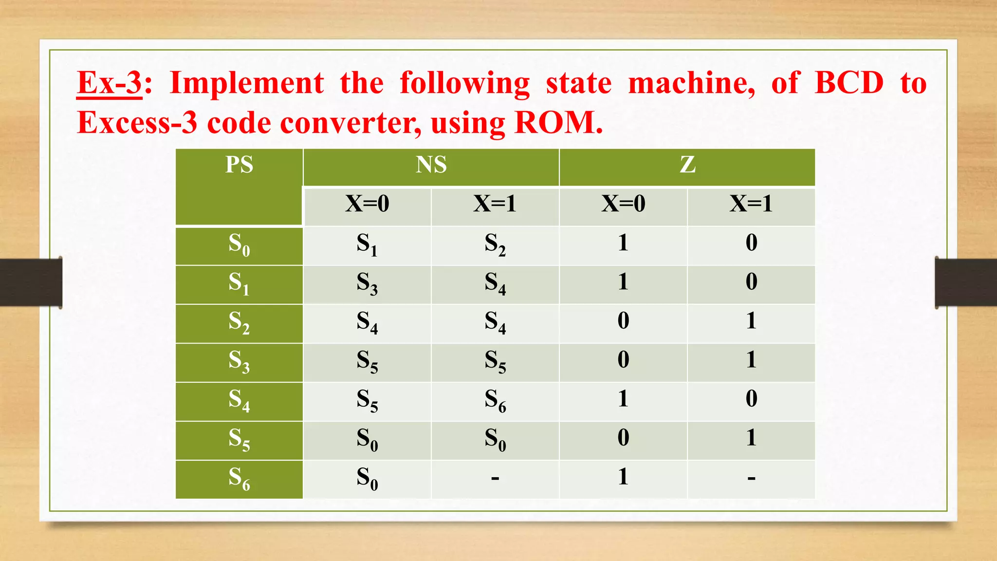
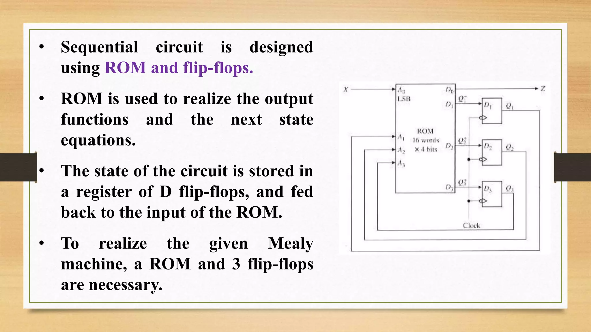
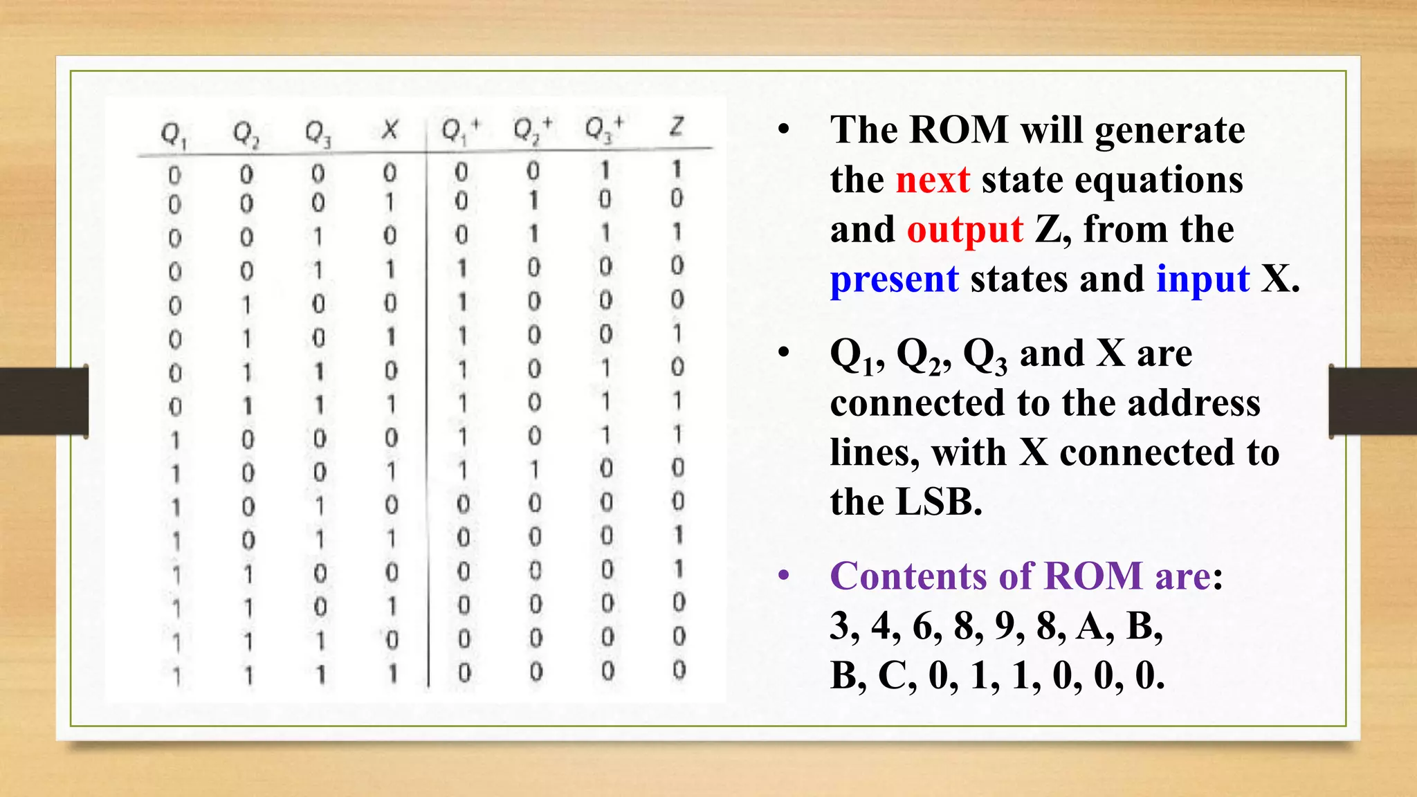
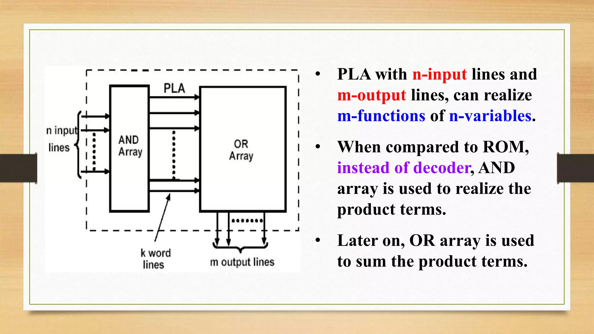
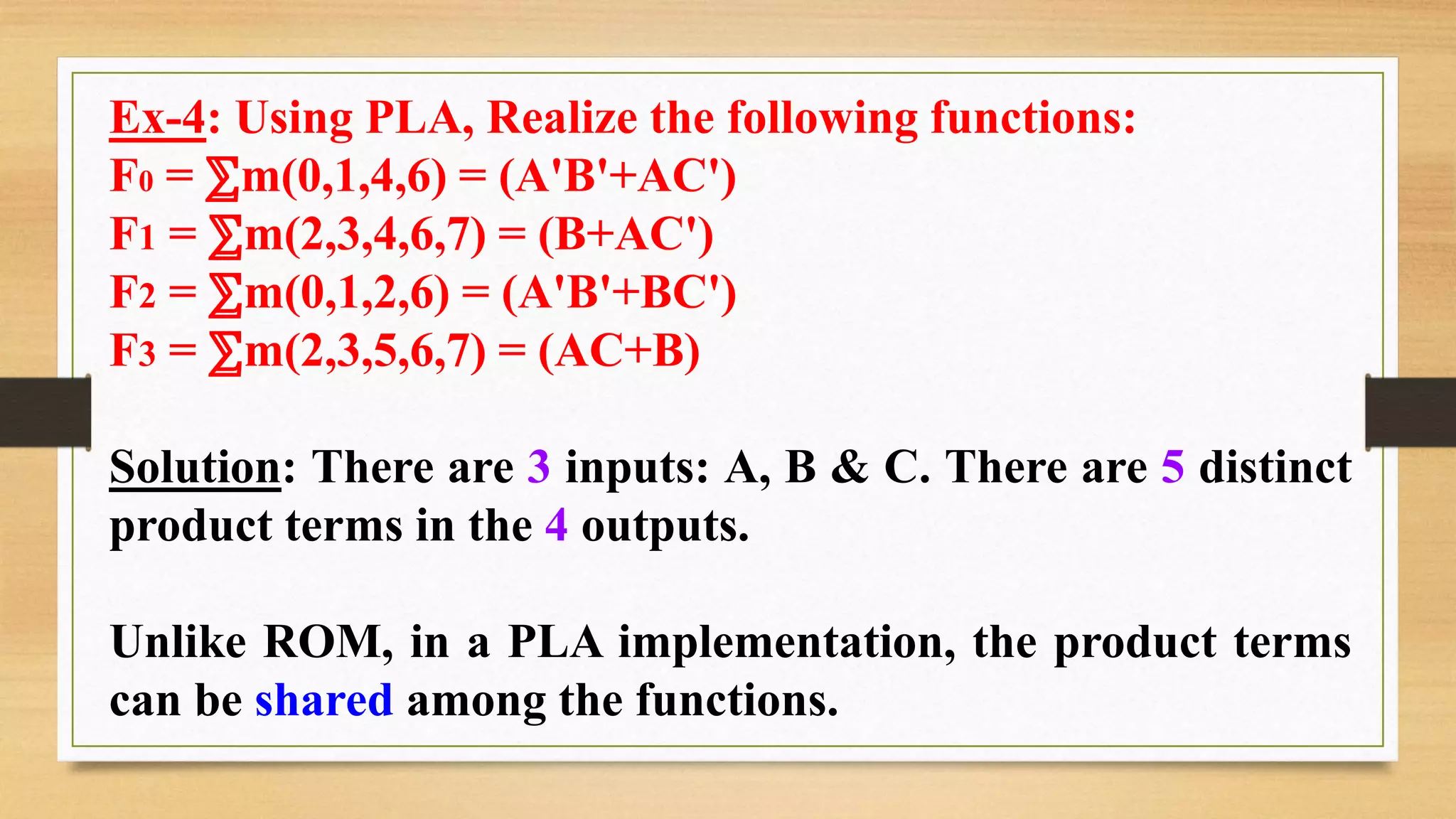
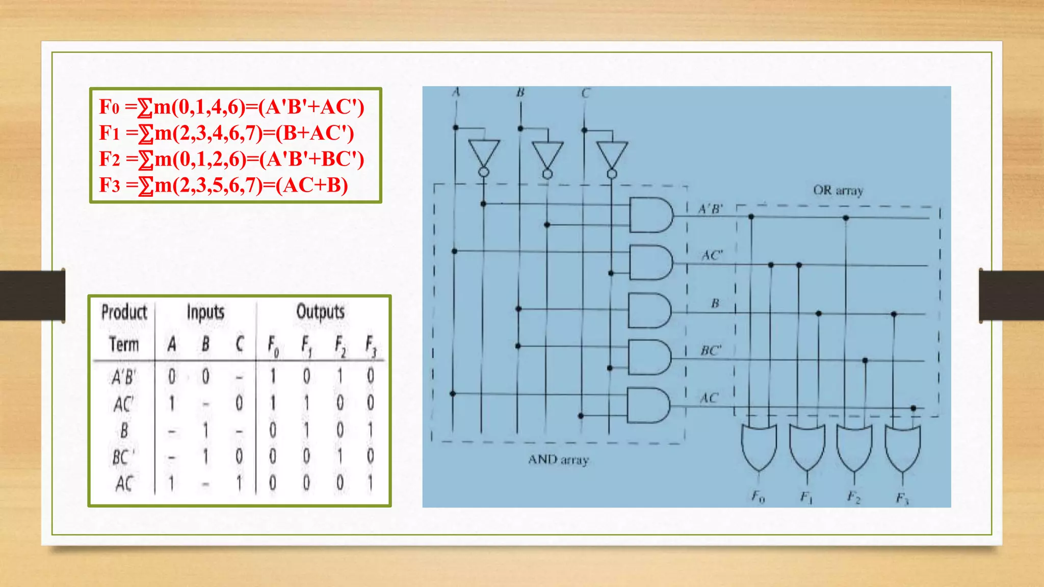
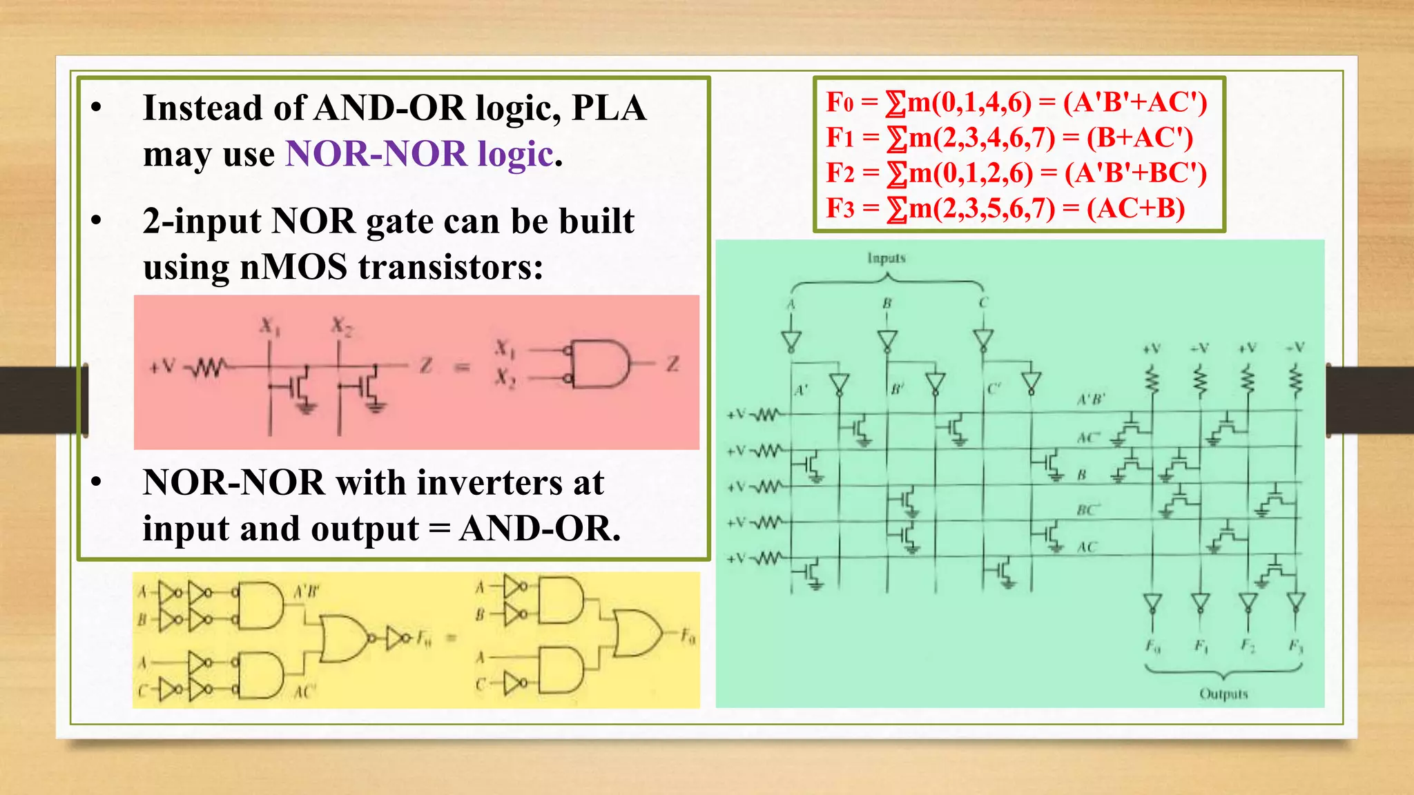


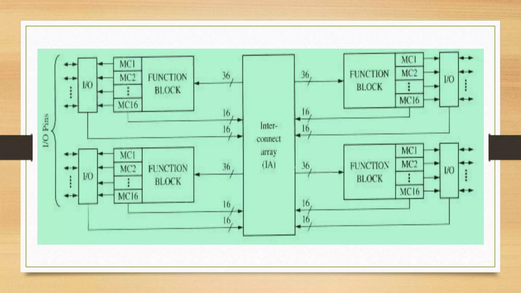
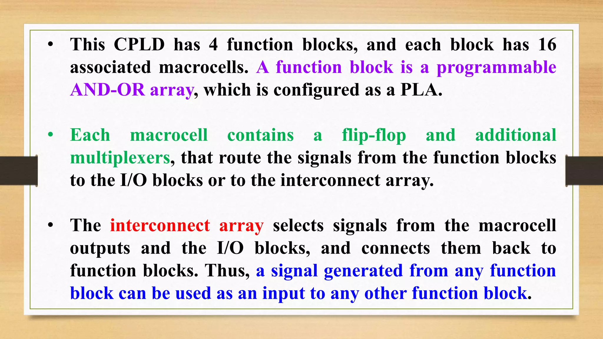
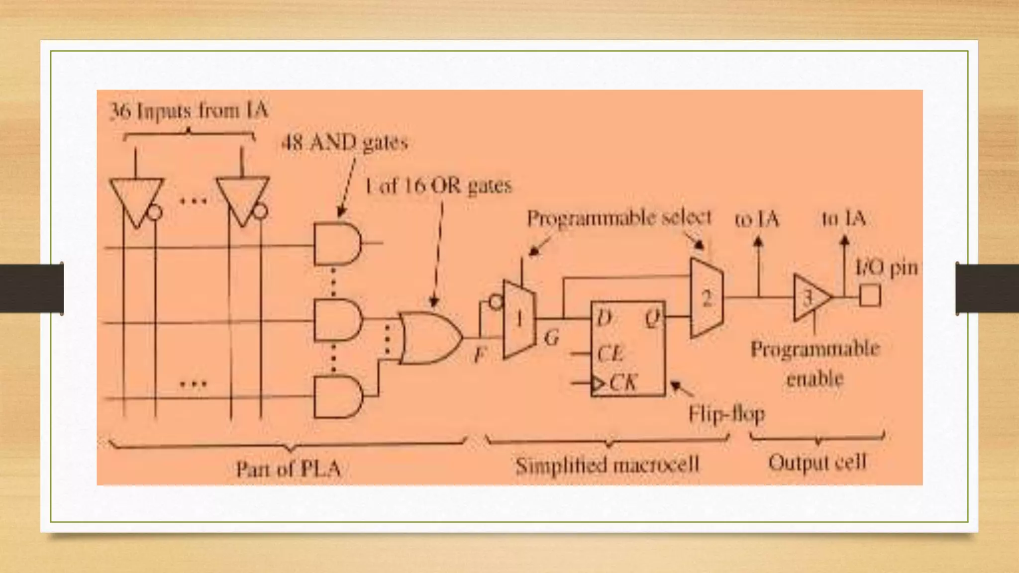
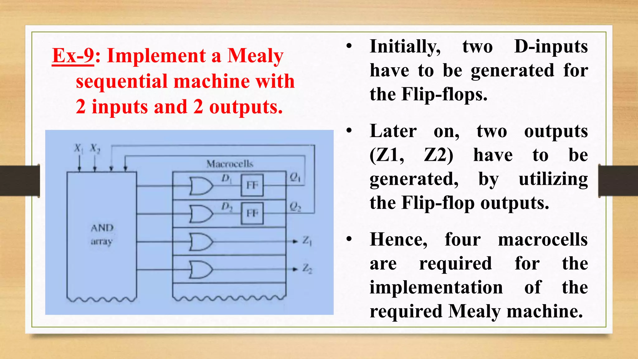
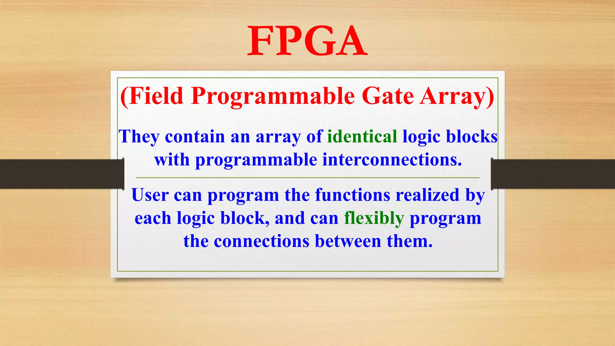
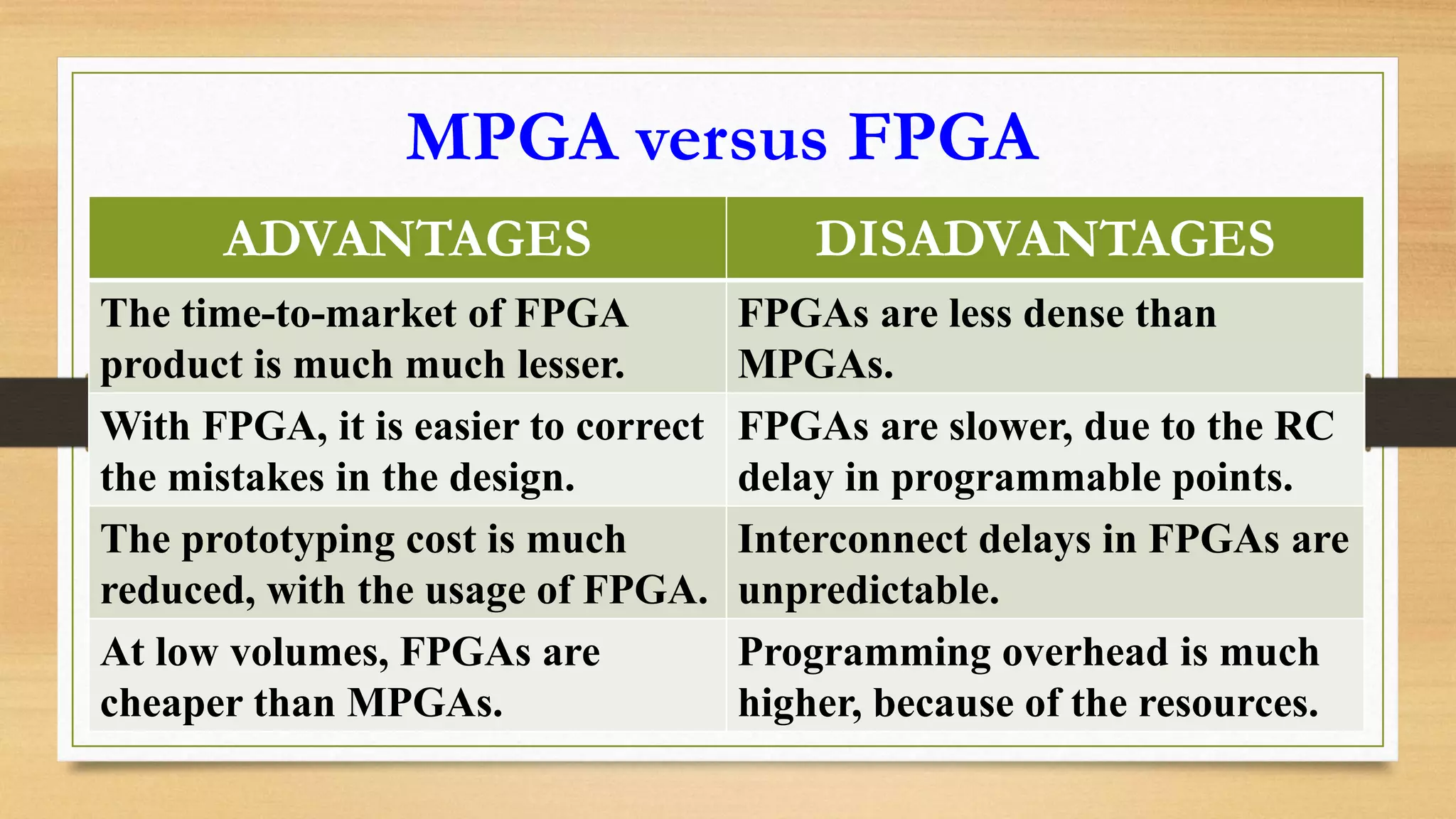
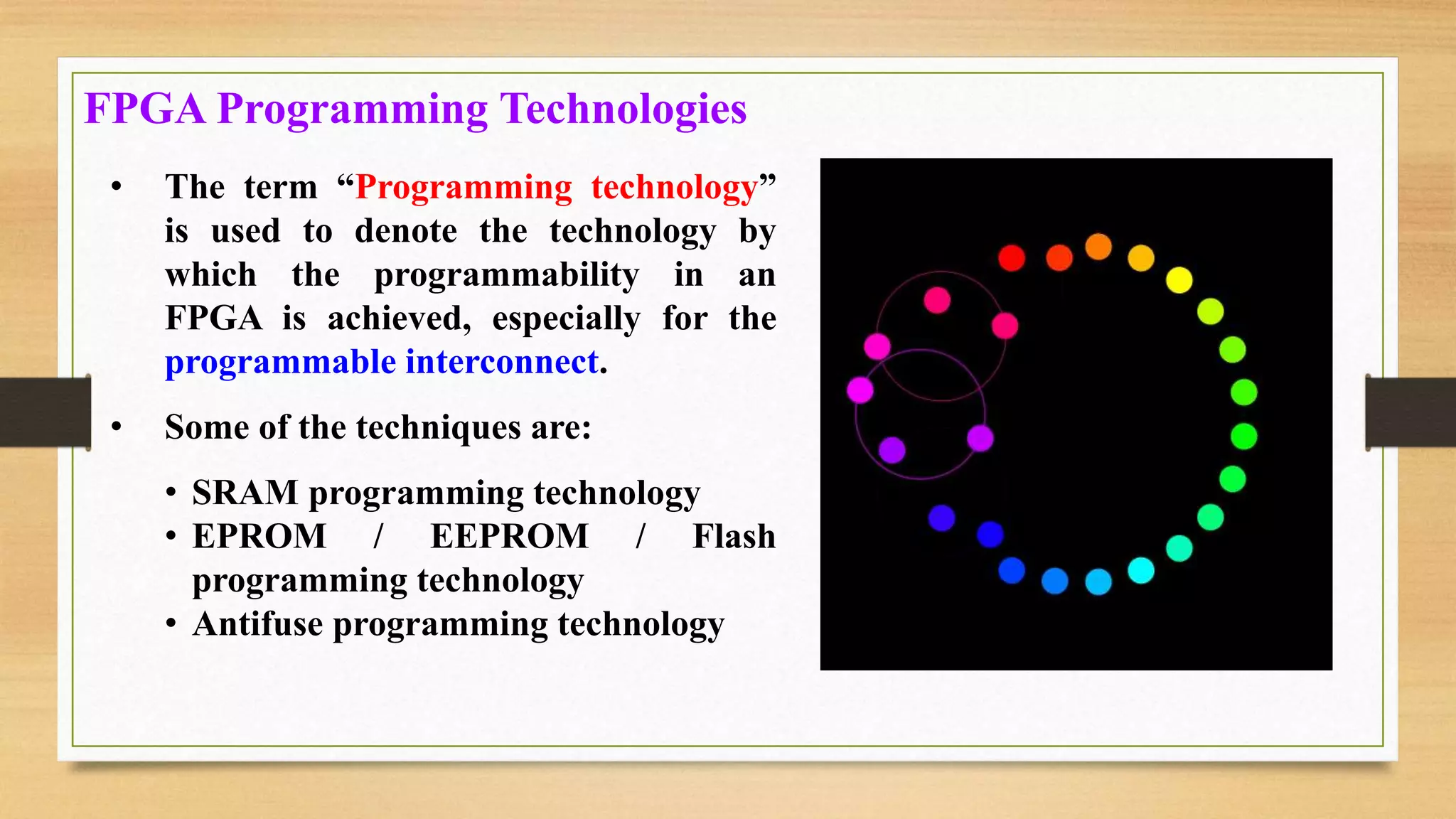
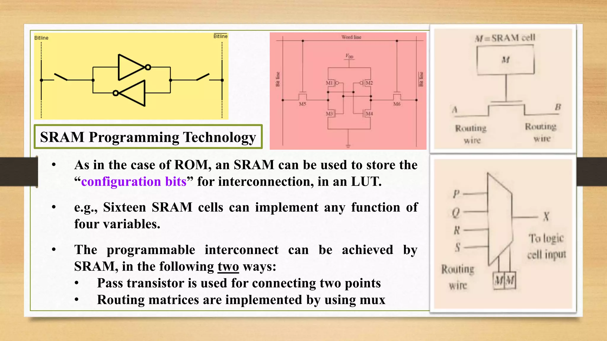
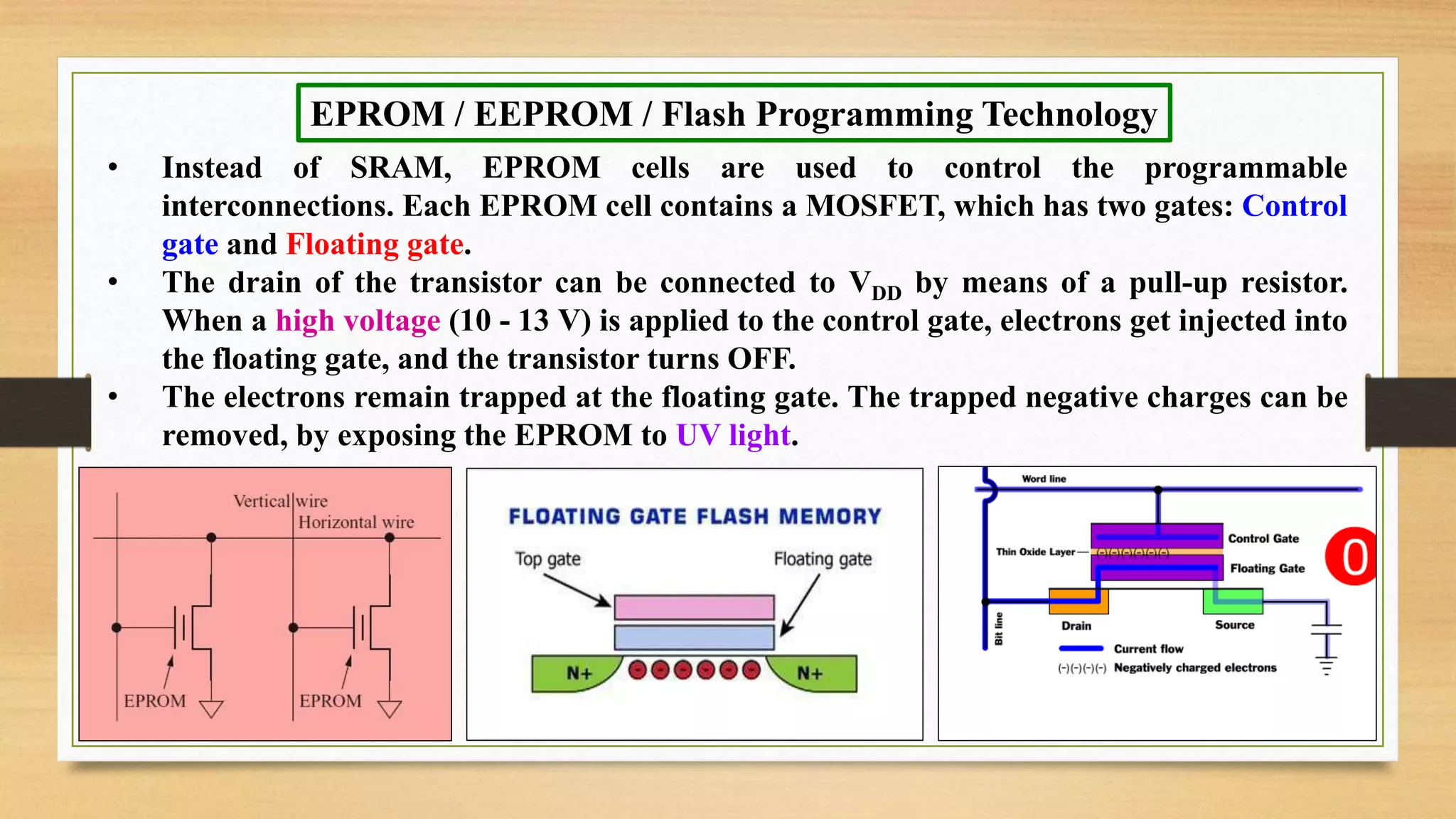
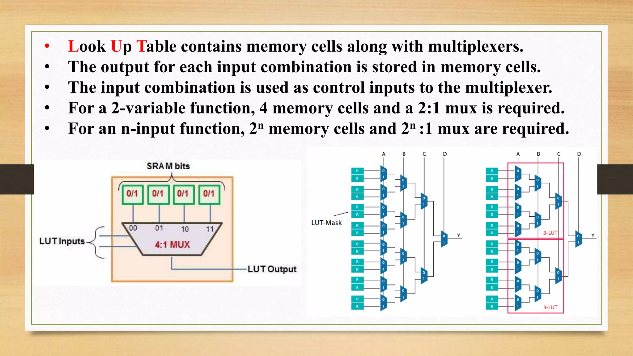
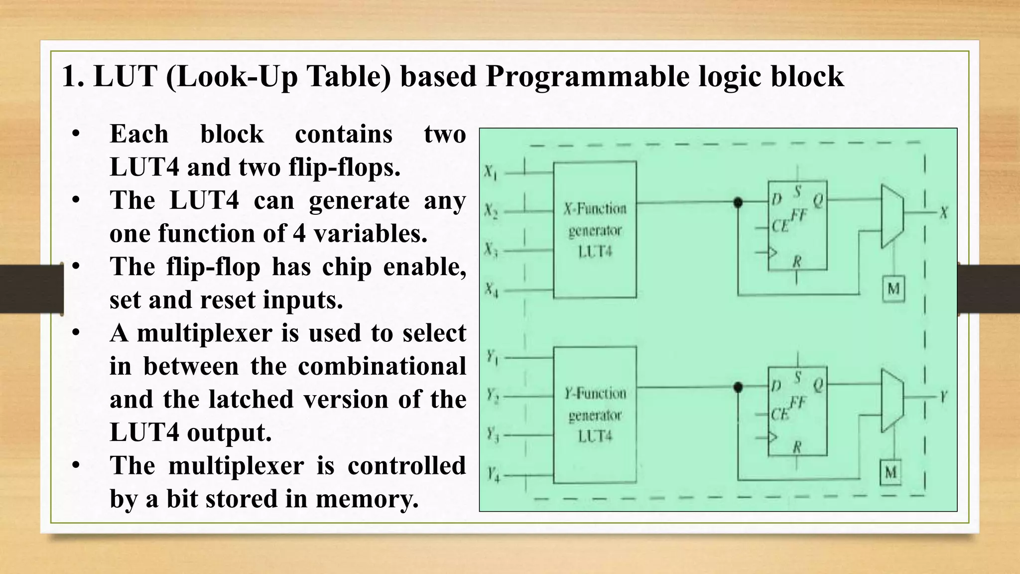
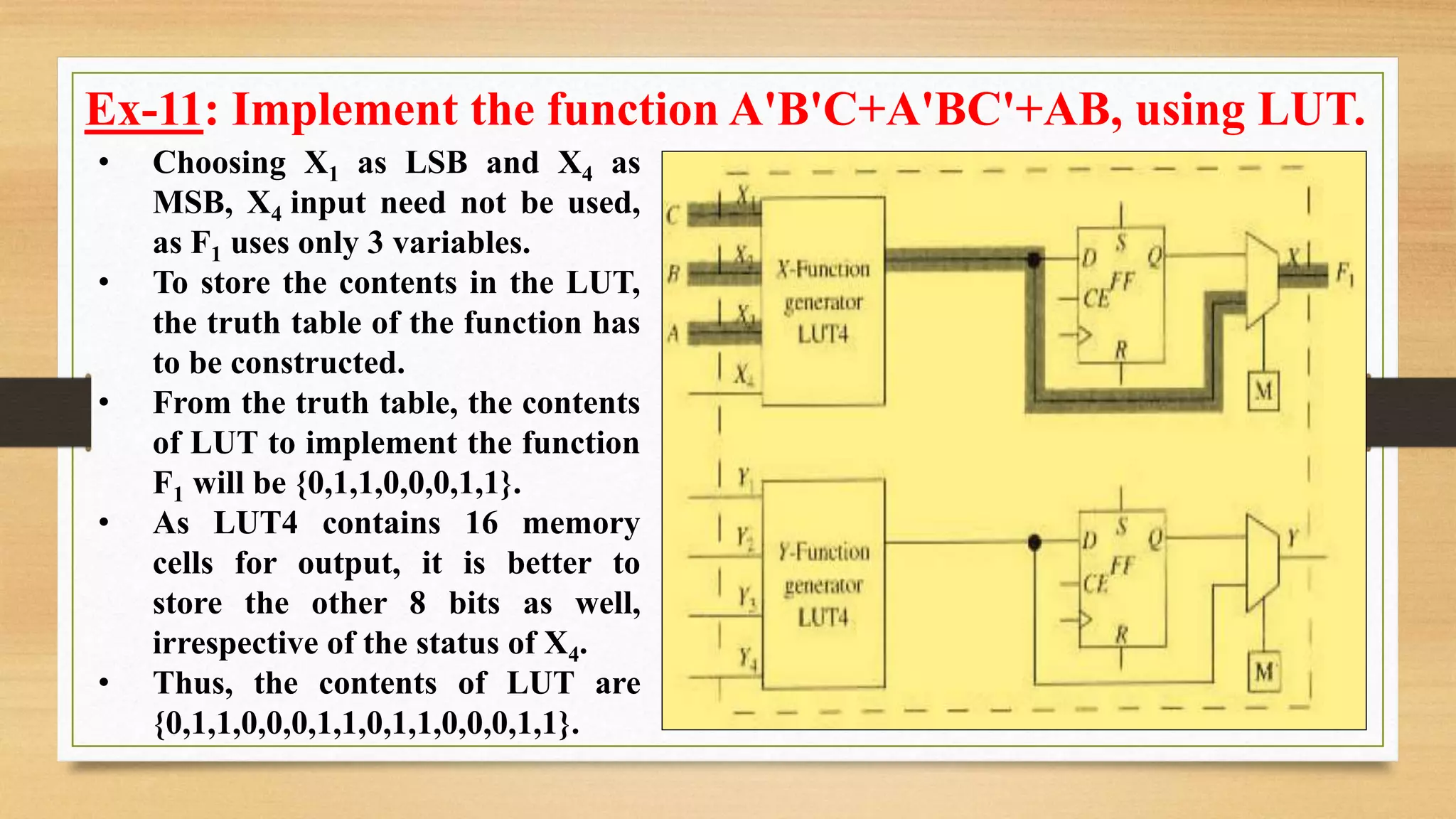
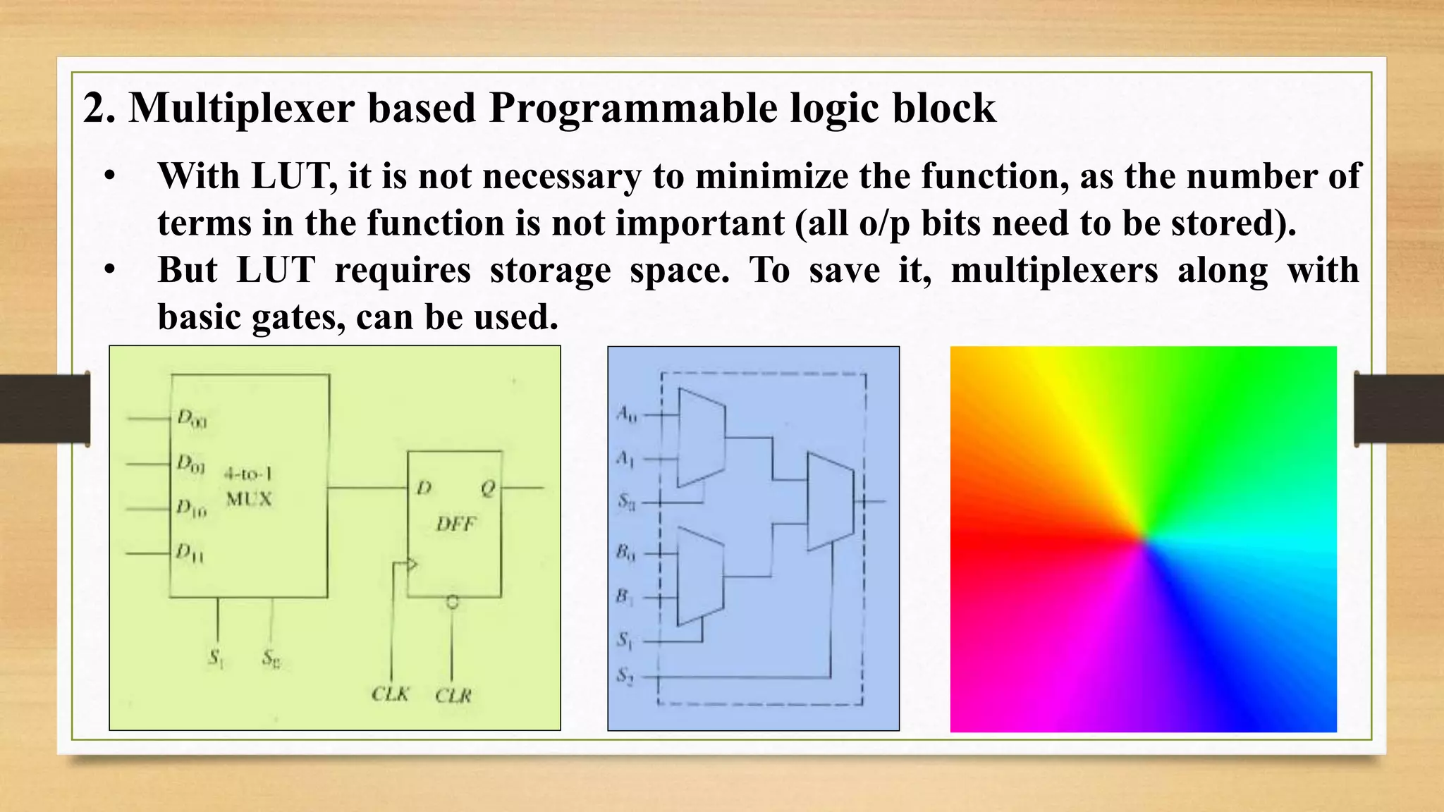
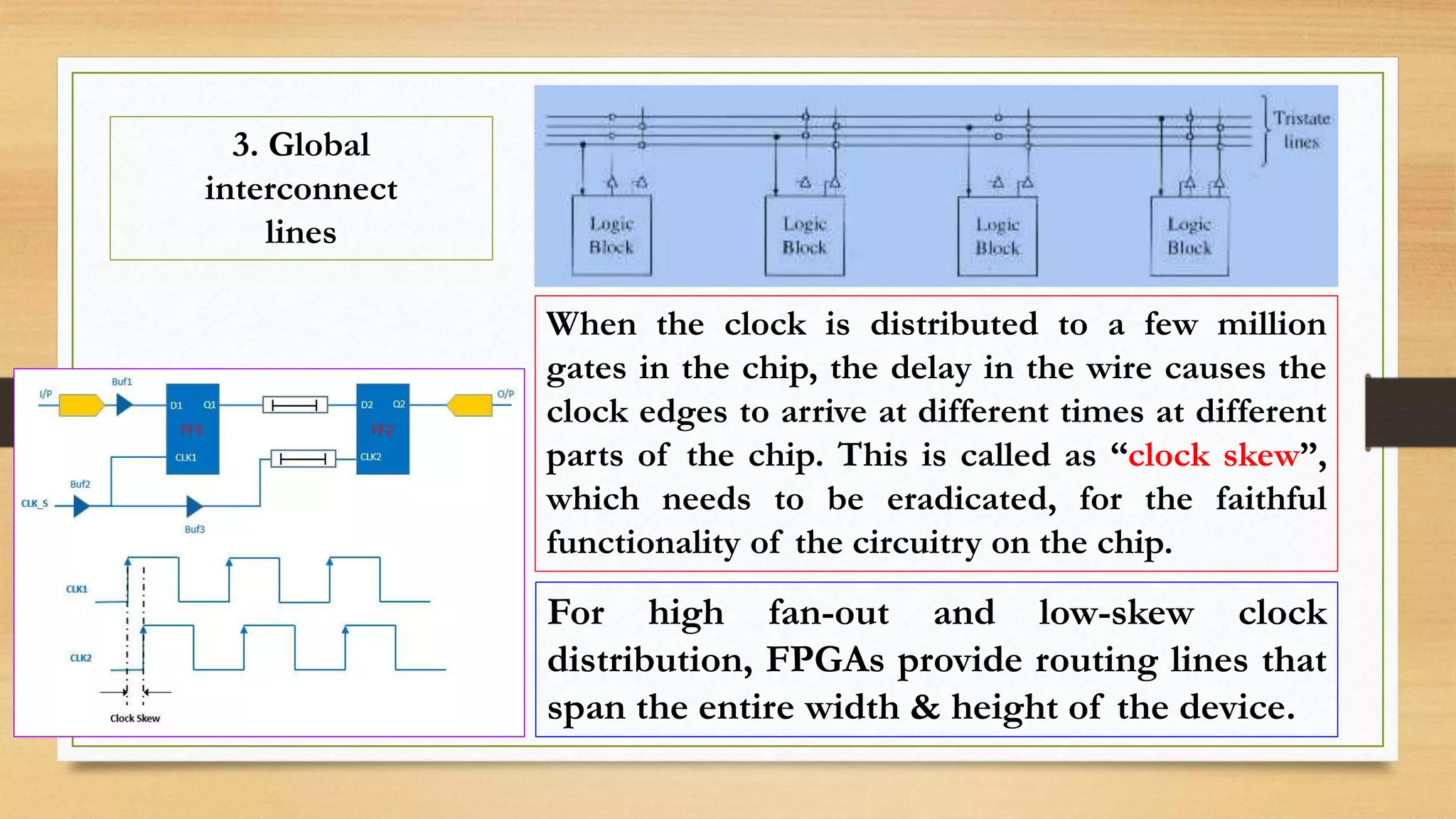
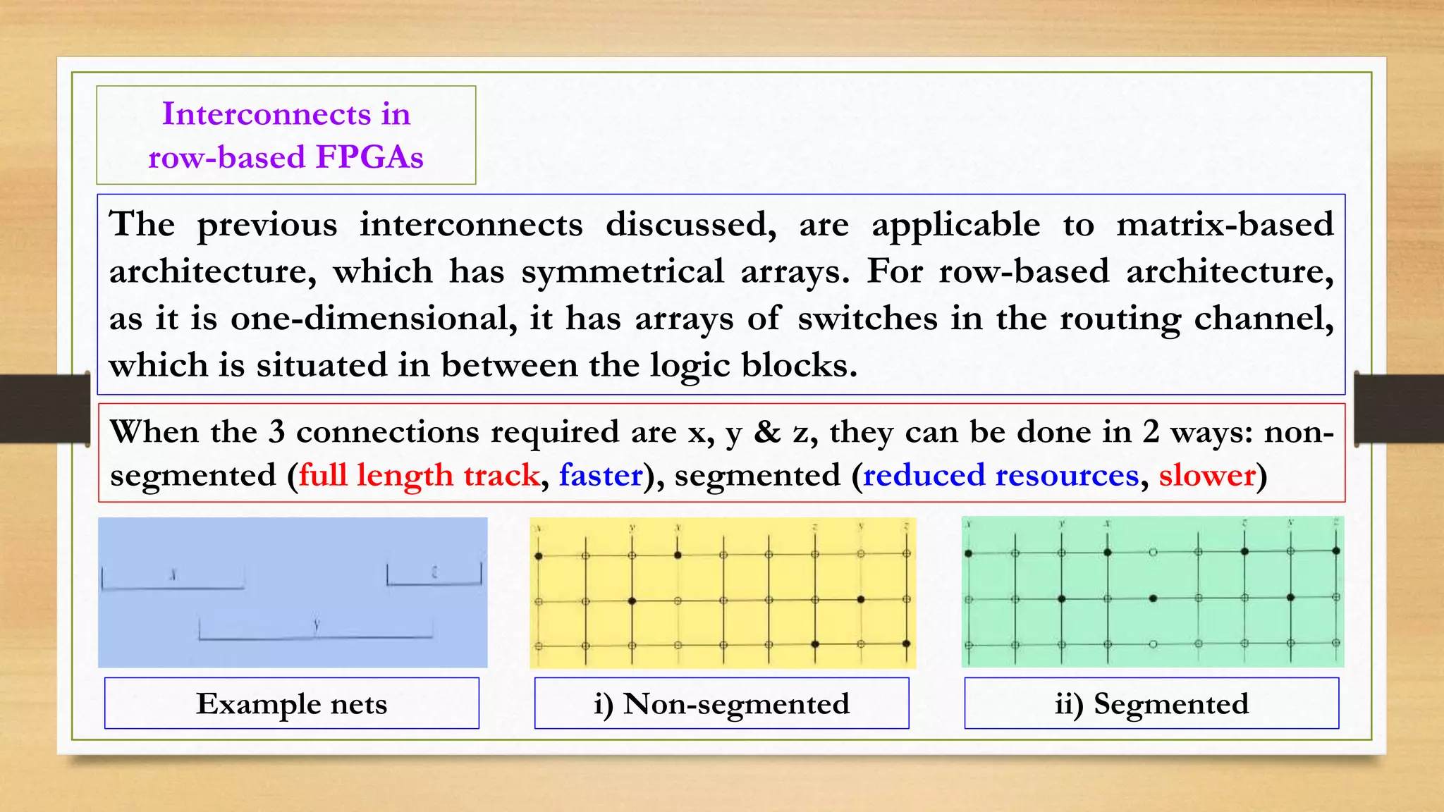
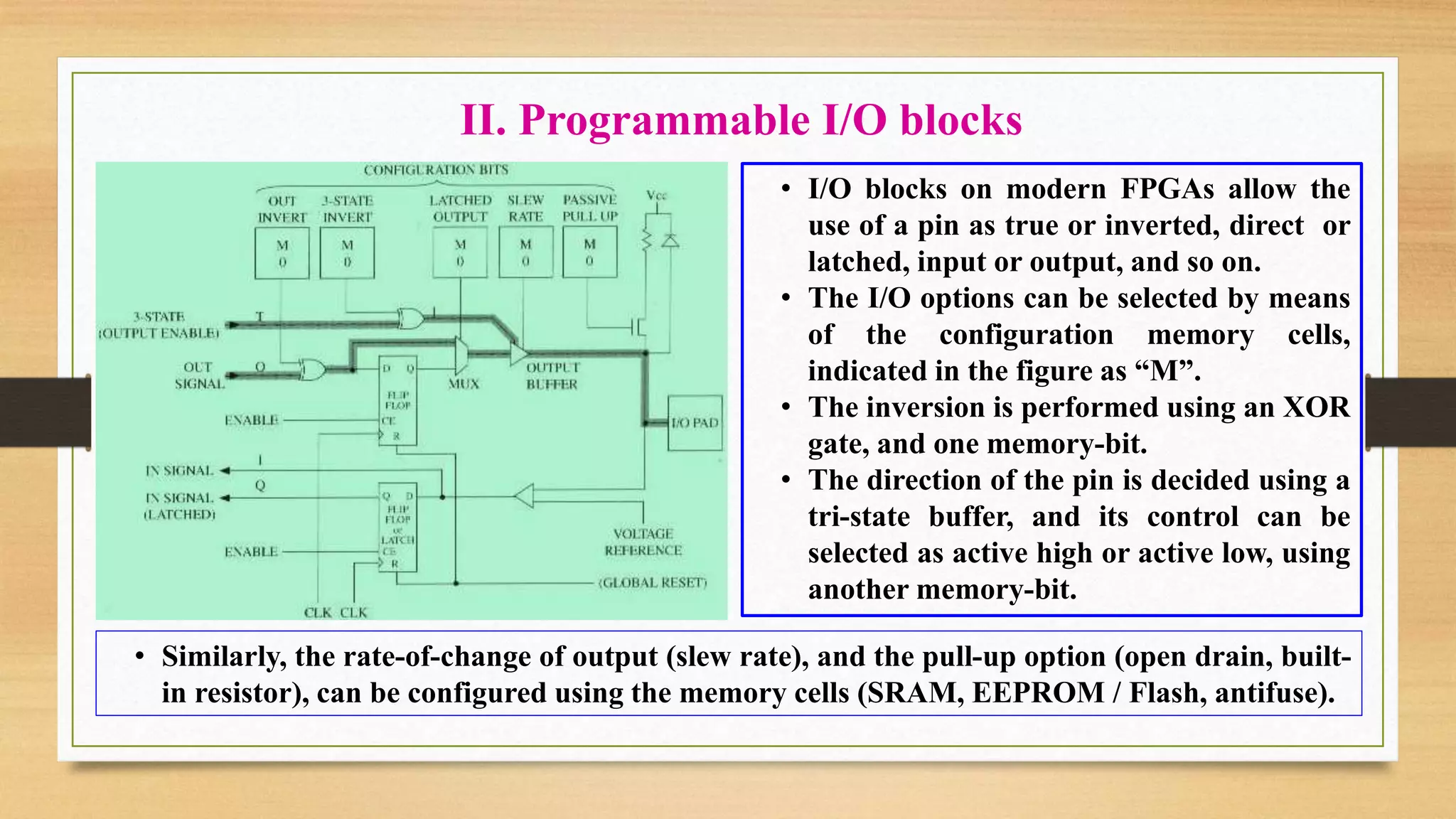
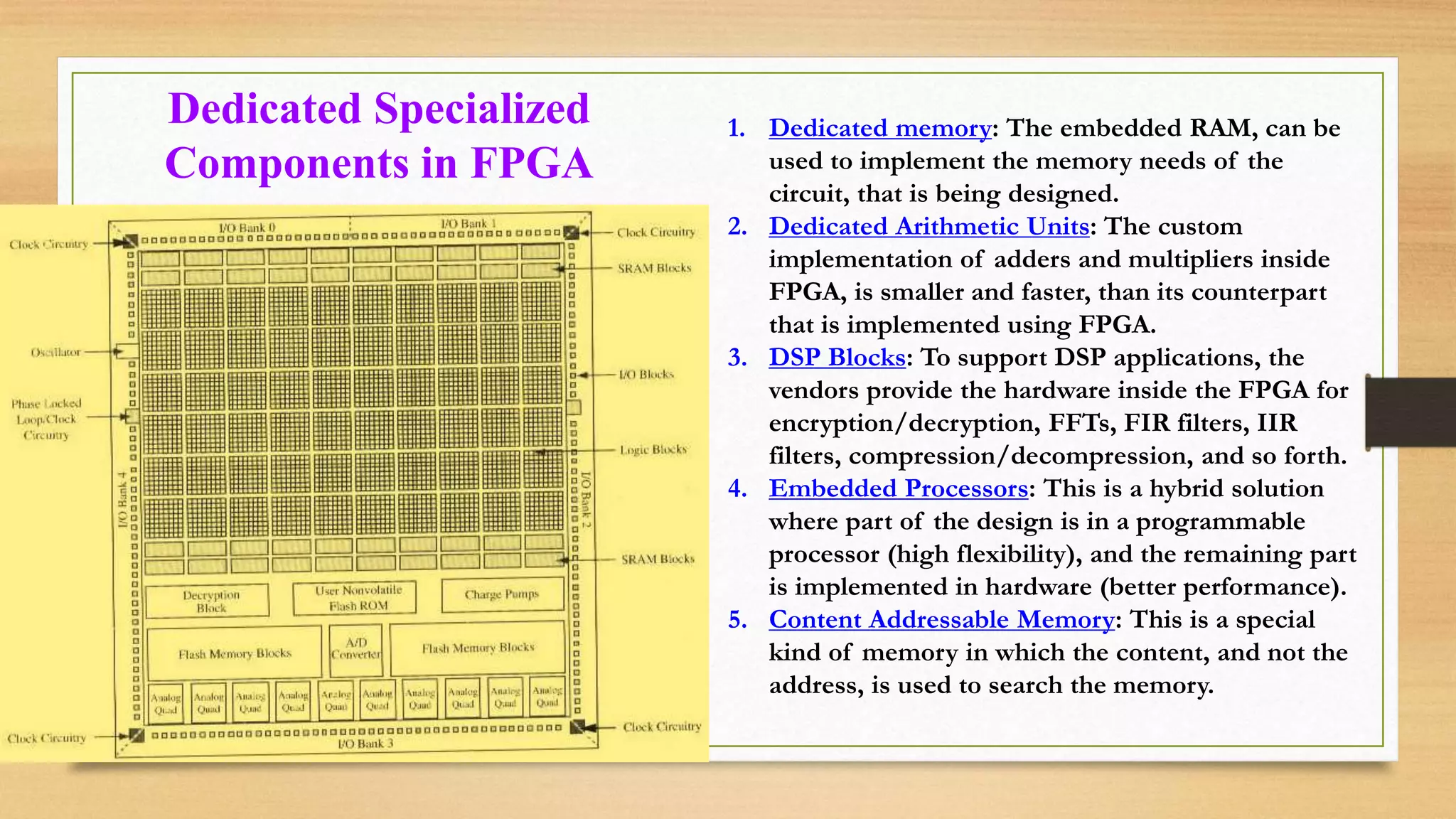
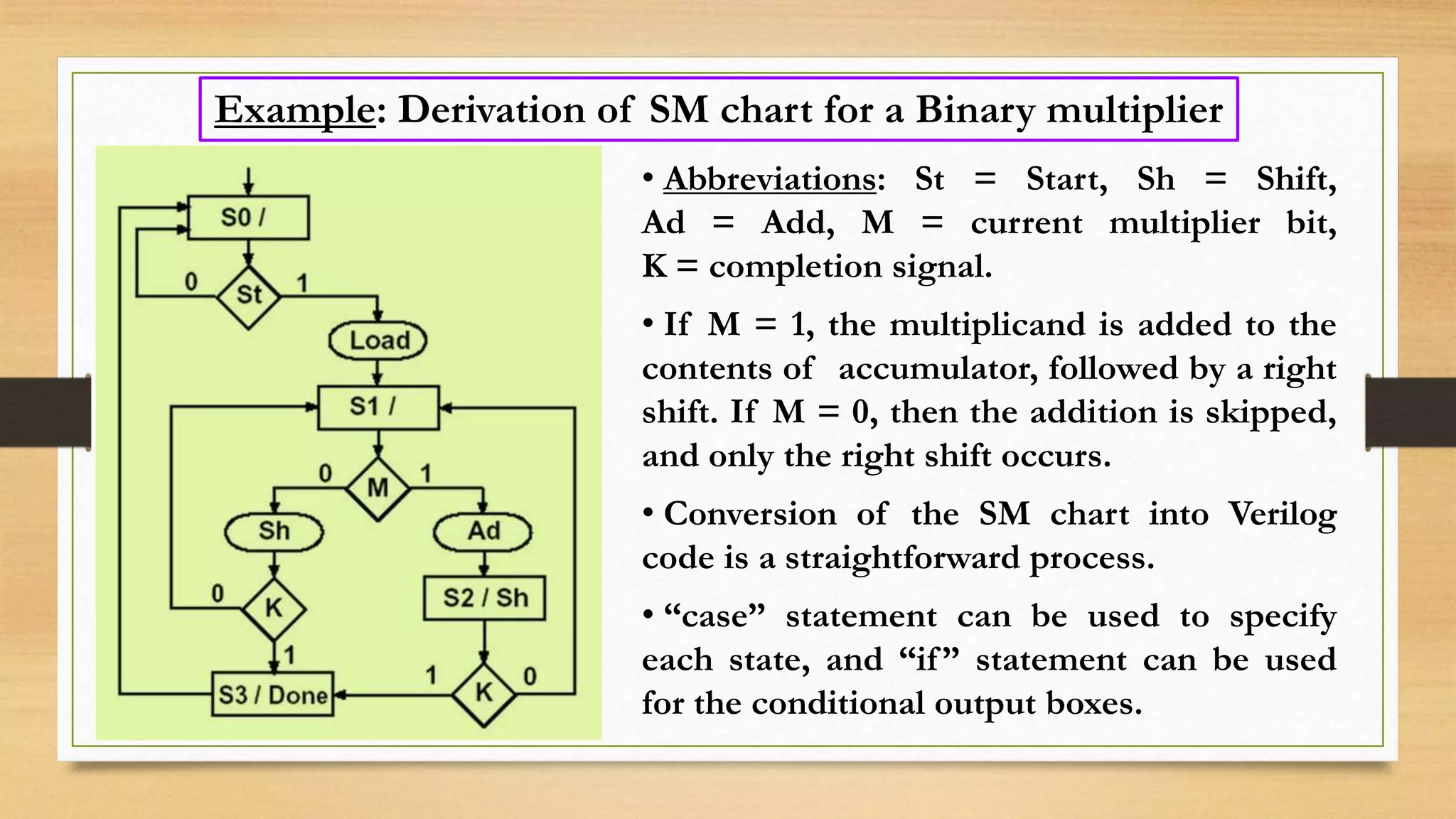


The document provides an overview of digital system design using hardware description language (HDL), focusing on programmable logic devices (PLDs), including various types such as ROM, FPGA, CPLD, PAL, and PLA. It discusses their functionalities, architectures, programming methods, and applications in implementing logic circuits. Additionally, it compares the advantages and disadvantages of different programmable logic devices regarding reprogrammability and performance characteristics.