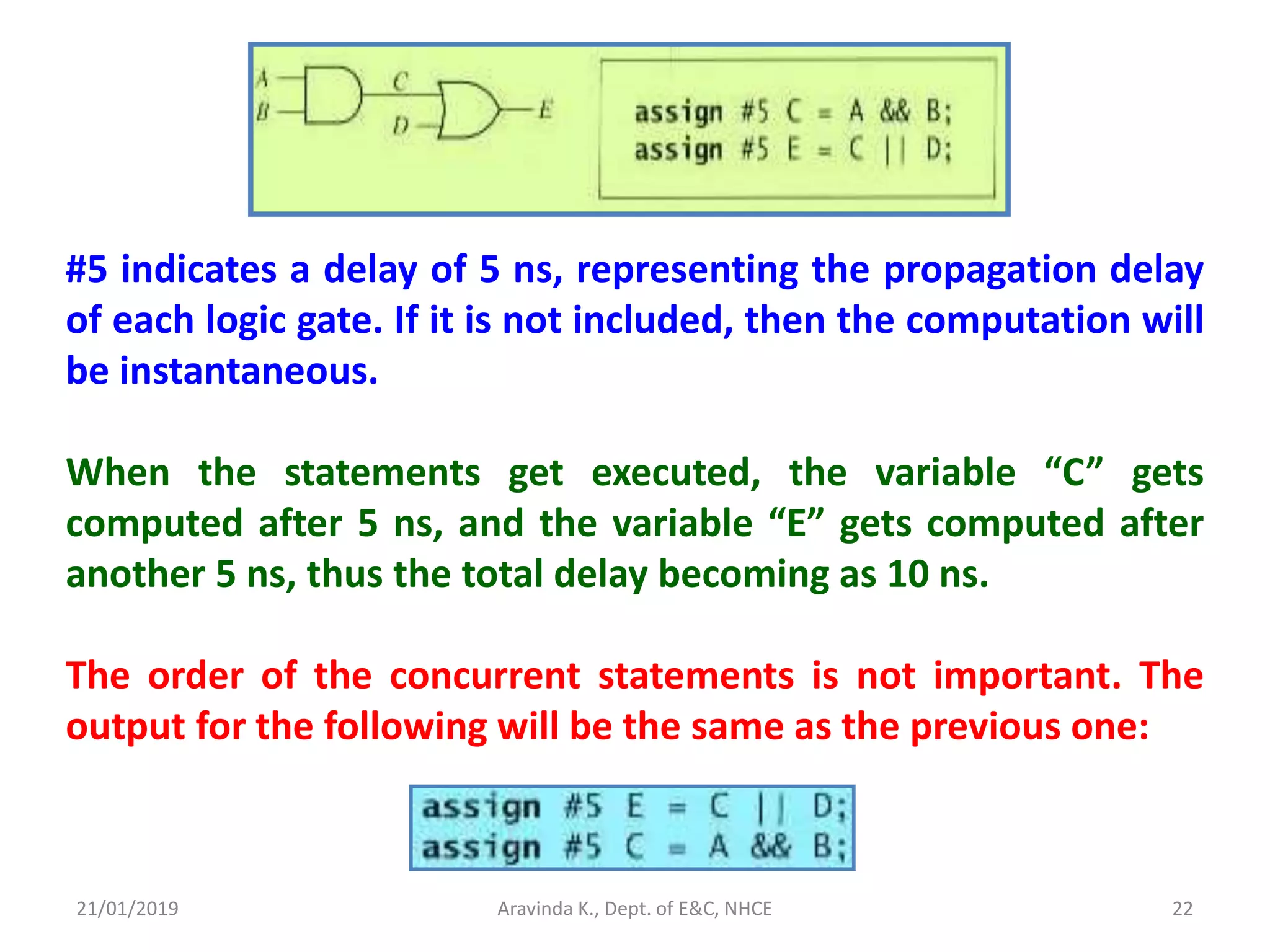
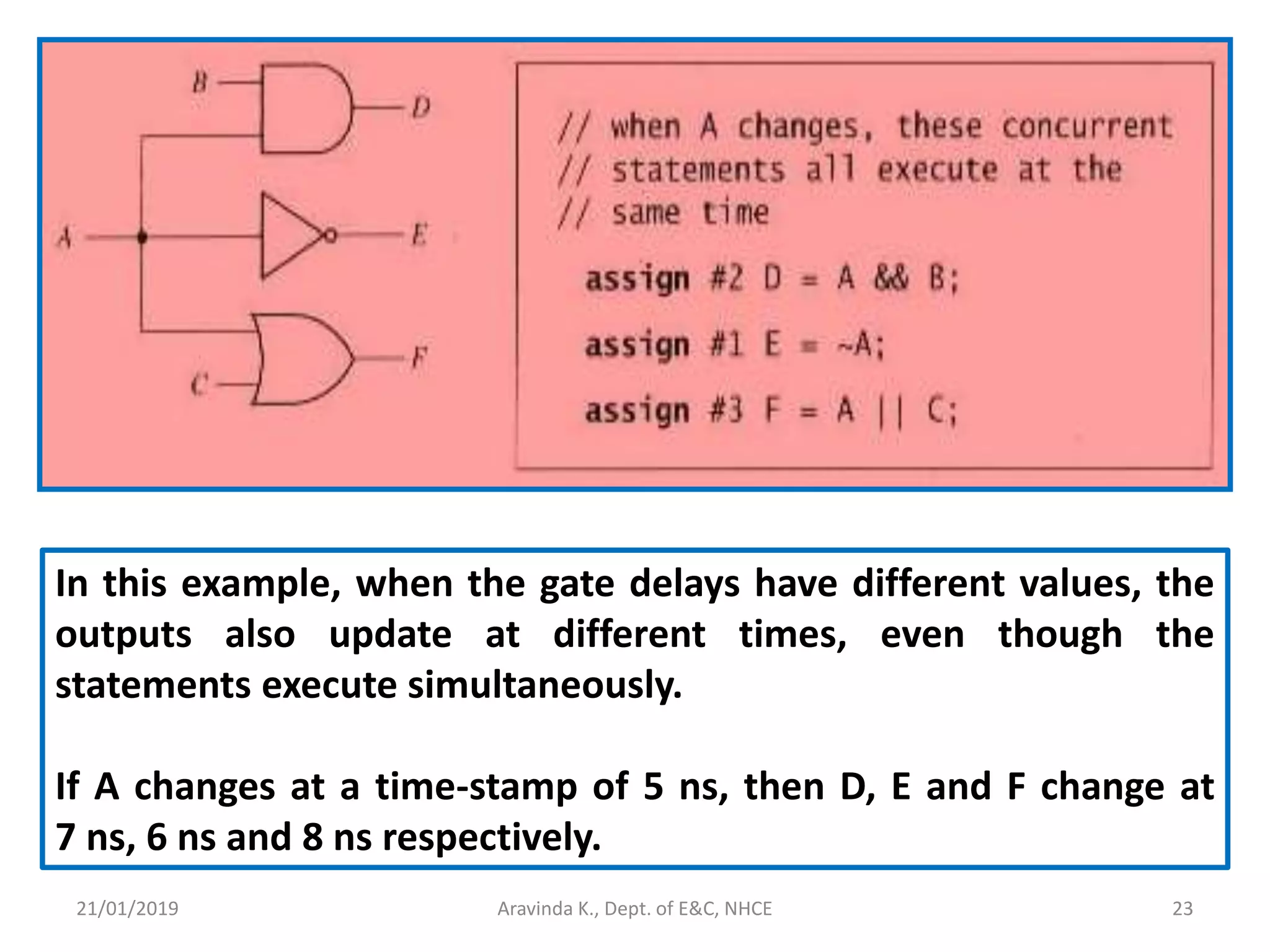
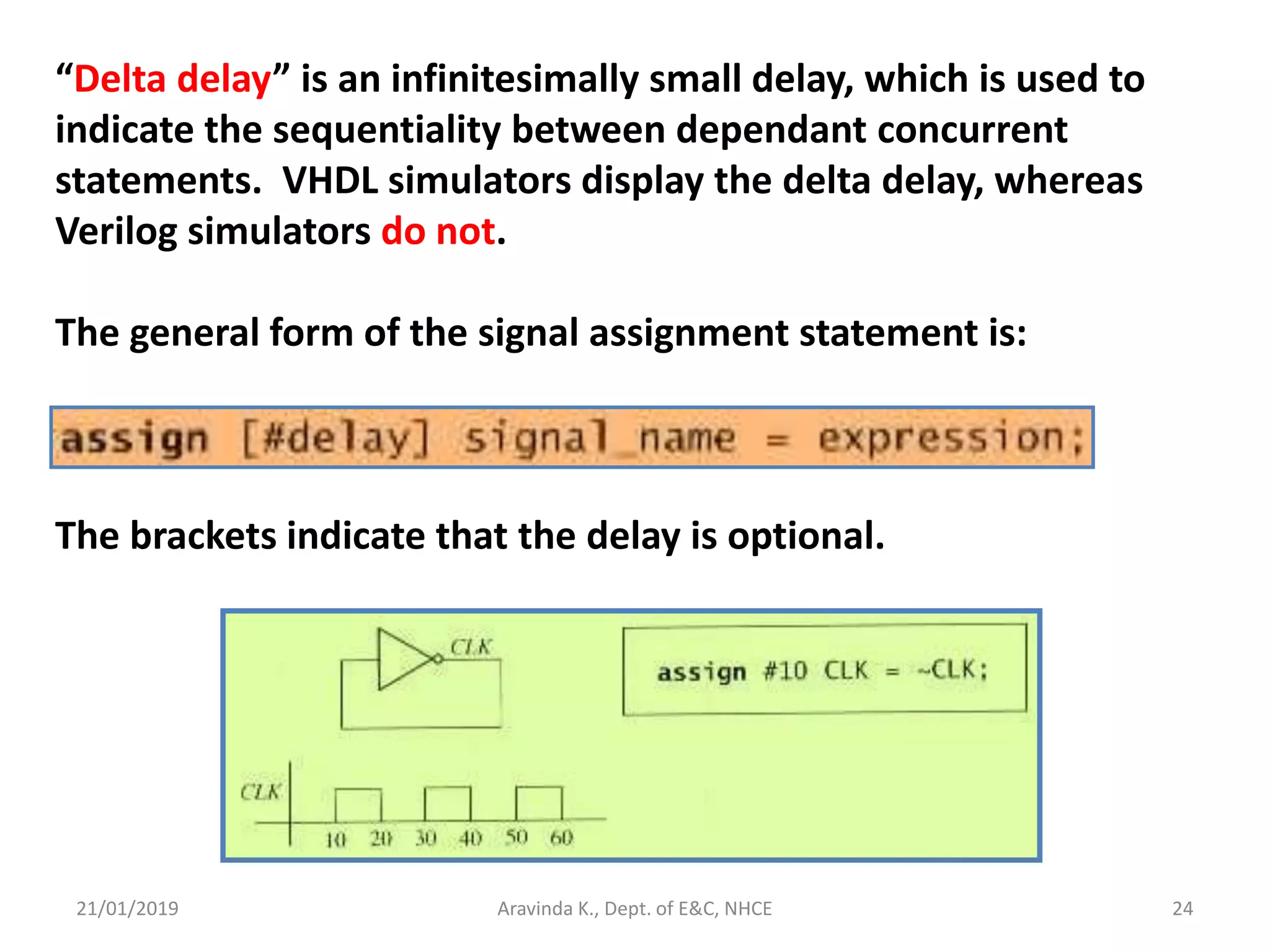
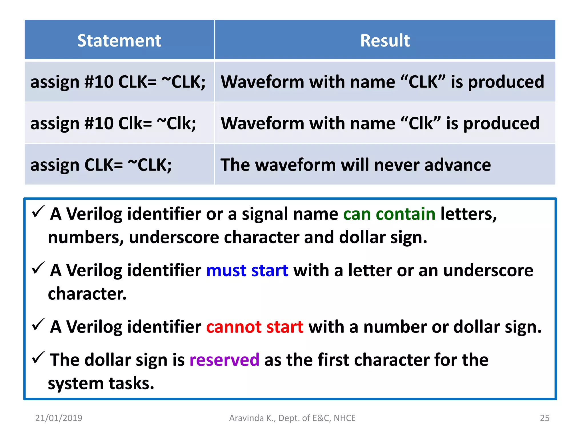
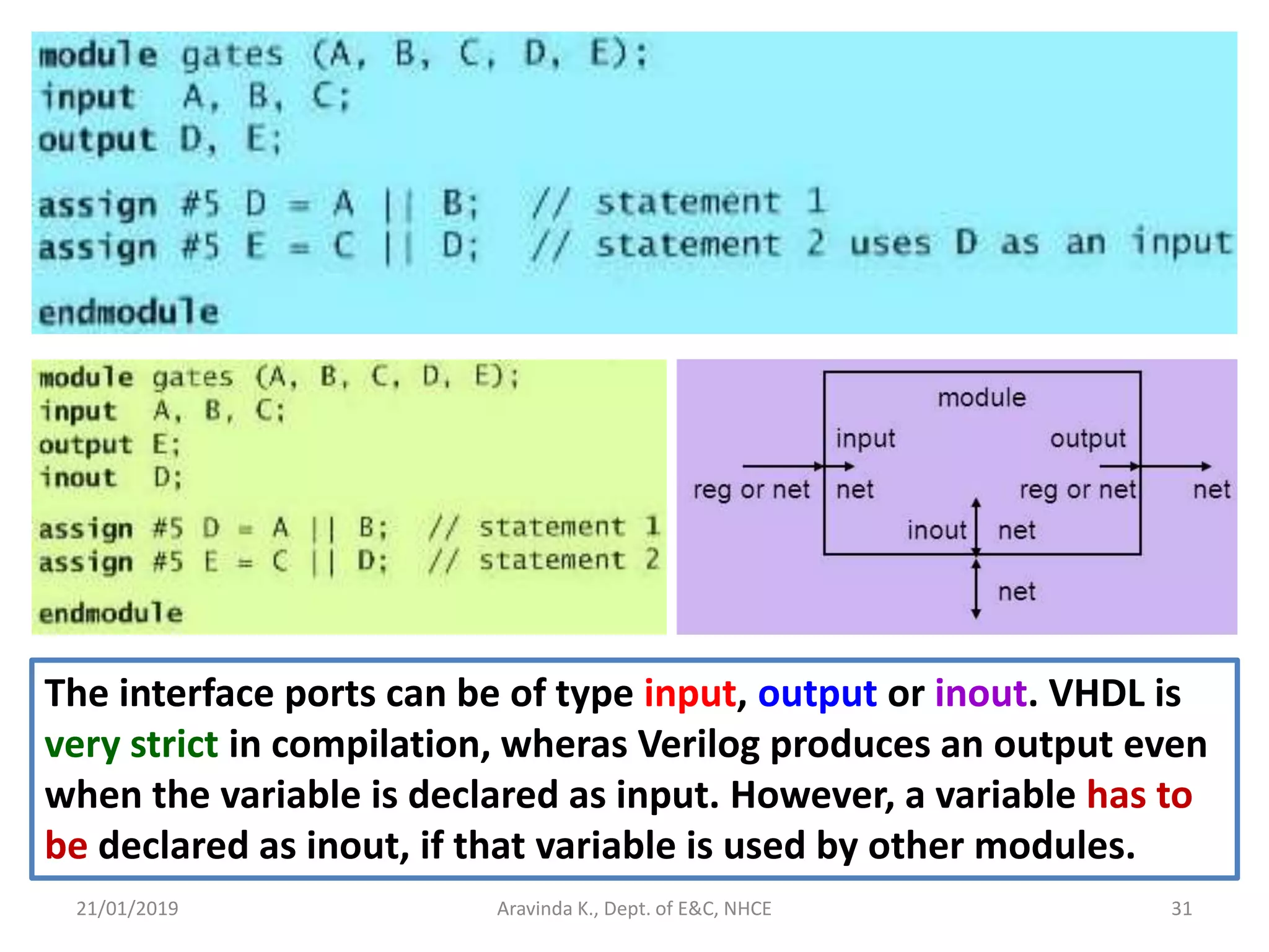
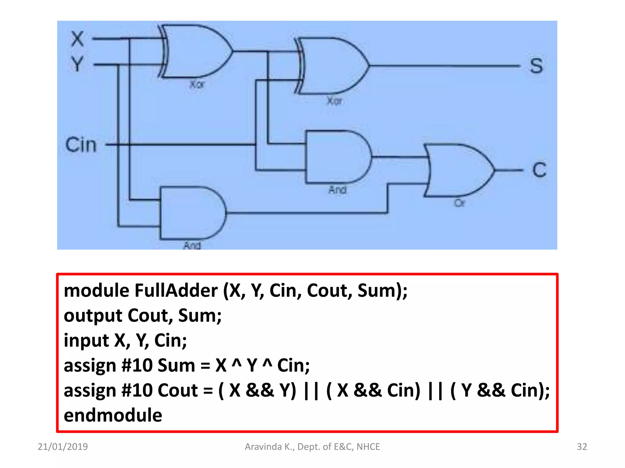
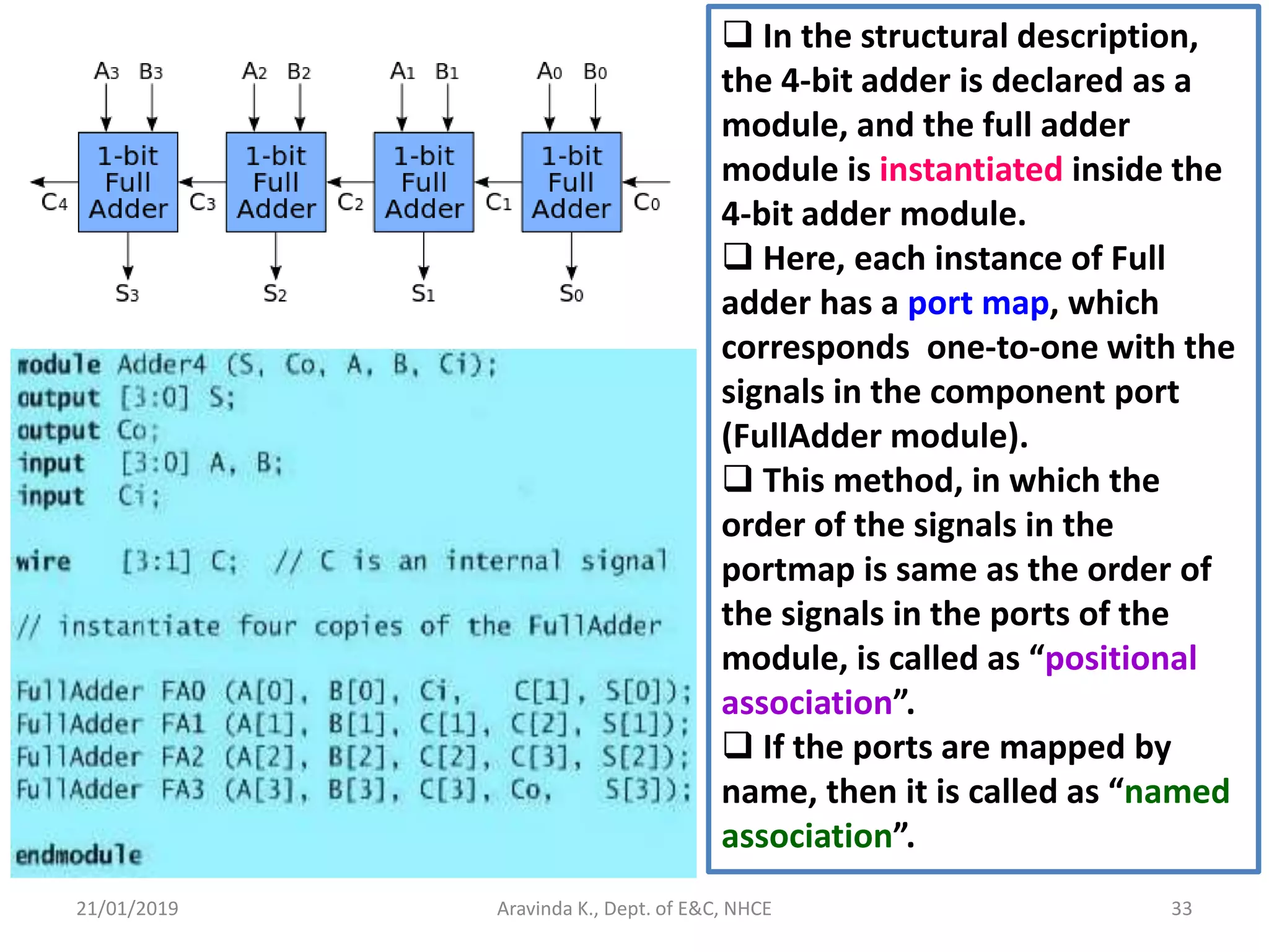
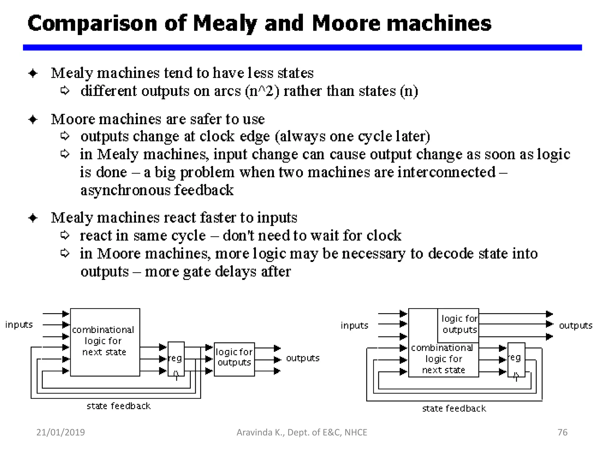
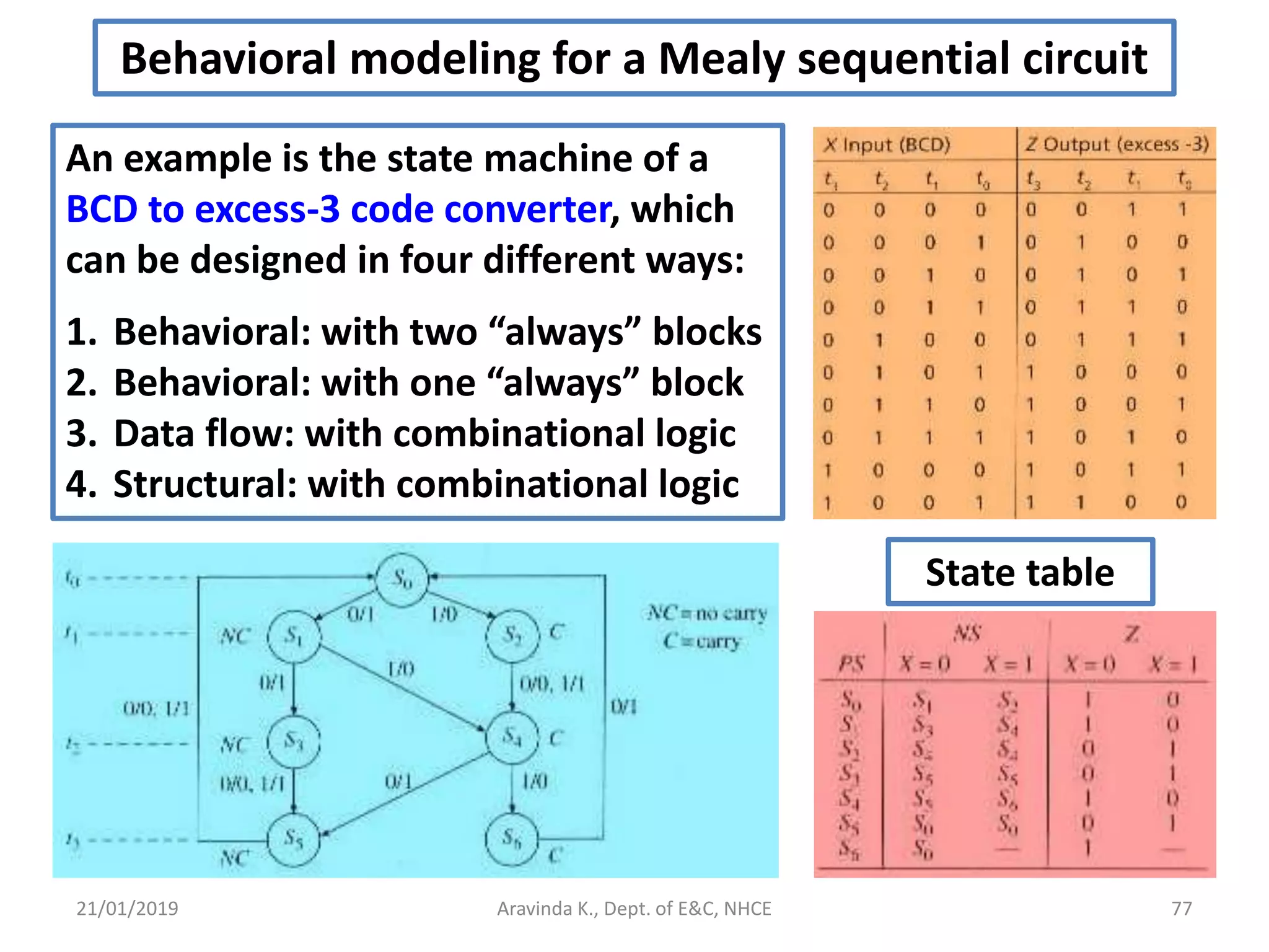
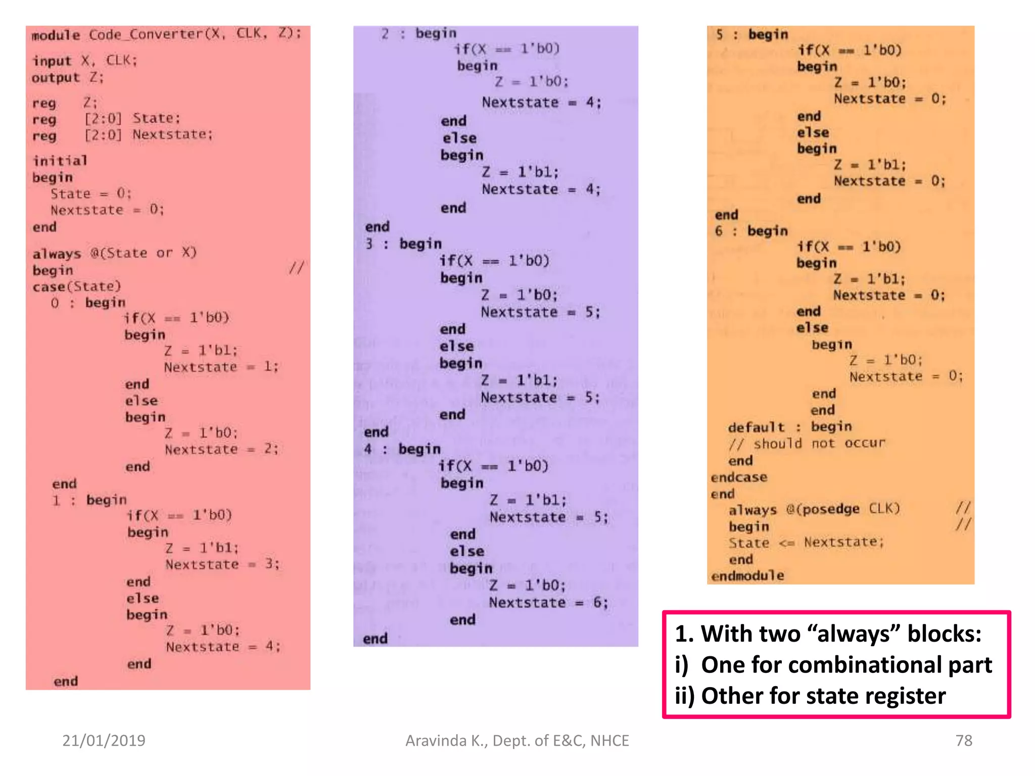
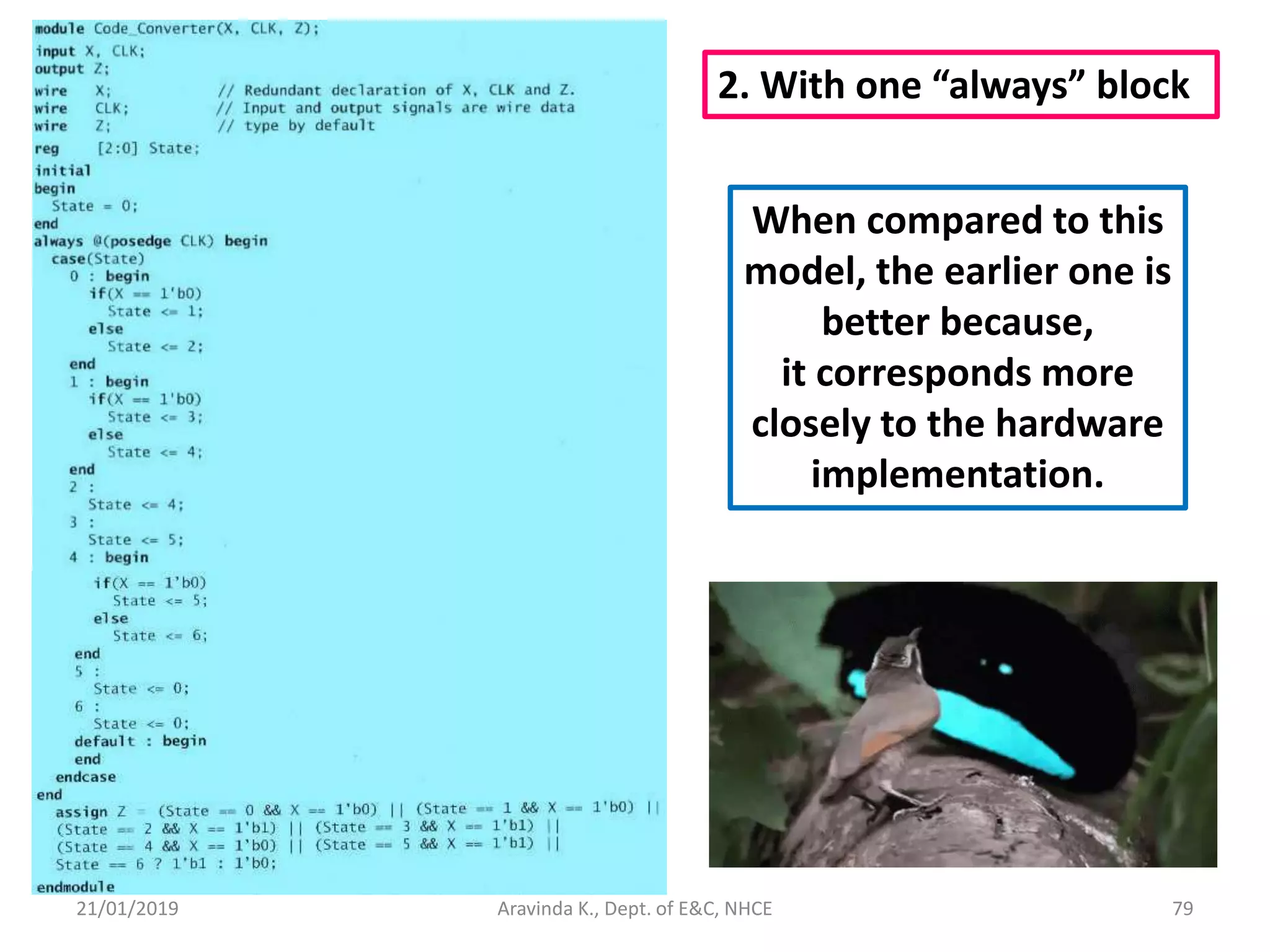
Download to read offline

![21/01/2019 27Aravinda K., Dept. of E&C, NHCE When the signal is of type wire (or net), it generally has a value of 0 or 1. The net values in Verilog are represented as - <number of bits>’<base><value>. Hence, 1’b0 means “1 position binary 0”. The decimal and hexadecimal values are represented with “d” and “h”. A one-dimensional array of bit signals is referred to as a vector. A 4 bit-wire can be named as vector B, and can be declared as, wire B[3:0];. The vector B has an index range 0 through 3, and its elements are designated as B[0], B[1], B[2] and B[3]. The statement B=4’b1100 assigns 1 to B[3], 1 to B[2], 0 to B[1] and 0 to B[0].](https://image.slidesharecdn.com/sdhdlece43-m1-200302071630/75/System-design-using-HDL-Module-1-27-2048.jpg)
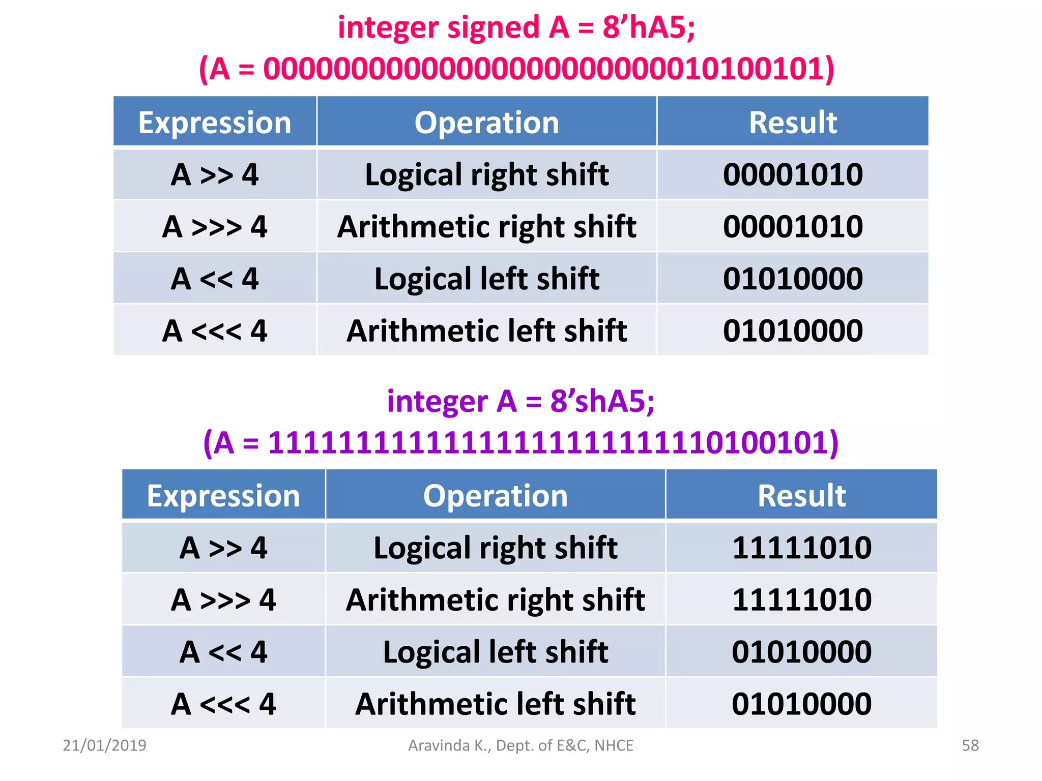
![21/01/2019 57Aravinda K., Dept. of E&C, NHCE Expression Operation Result A >> 4 Logical right shift 00001010 A >>> 4 Arithmetic right shift 11111010 A << 4 Logical left shift 01010000 A <<< 4 Arithmetic left shift 01010000 reg signed [7:0] A = 8’hA5; (A = 10100101) Expression Operation Result B >> 4 Logical right shift 00001010 B >>> 4 Arithmetic right shift 00001010 B << 4 Logical left shift 01010000 B <<< 4 Arithmetic left shift 01010000 reg [7:0] B = 8’hA5; (B = 10100101)](https://image.slidesharecdn.com/sdhdlece43-m1-200302071630/75/System-design-using-HDL-Module-1-57-2048.jpg)
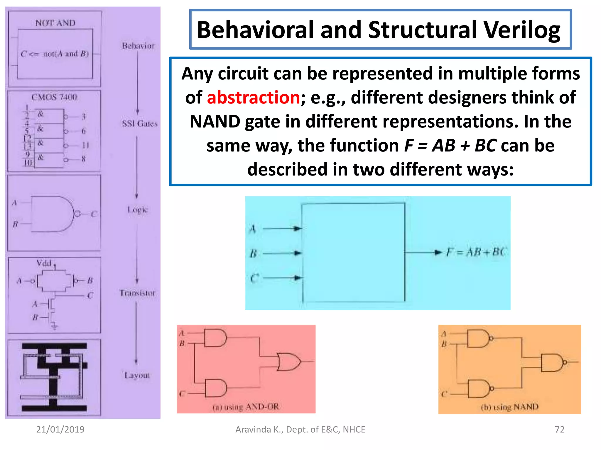
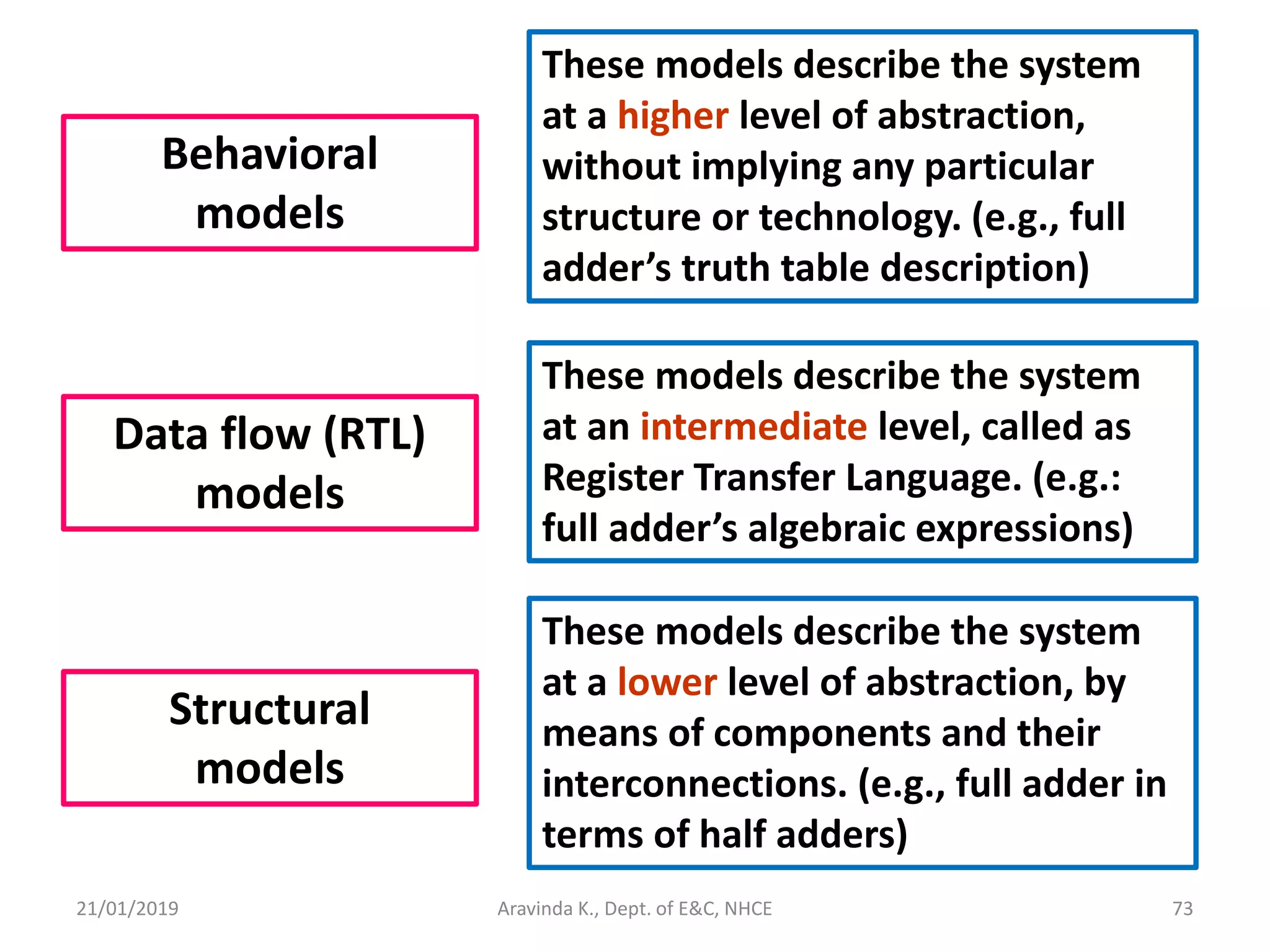


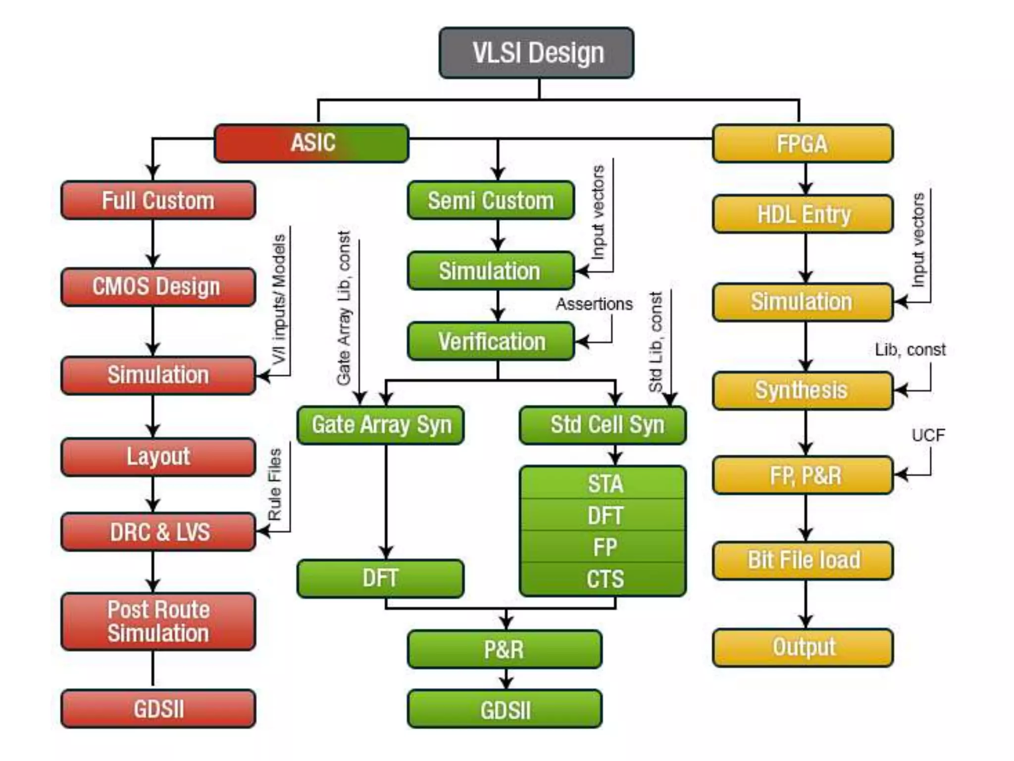
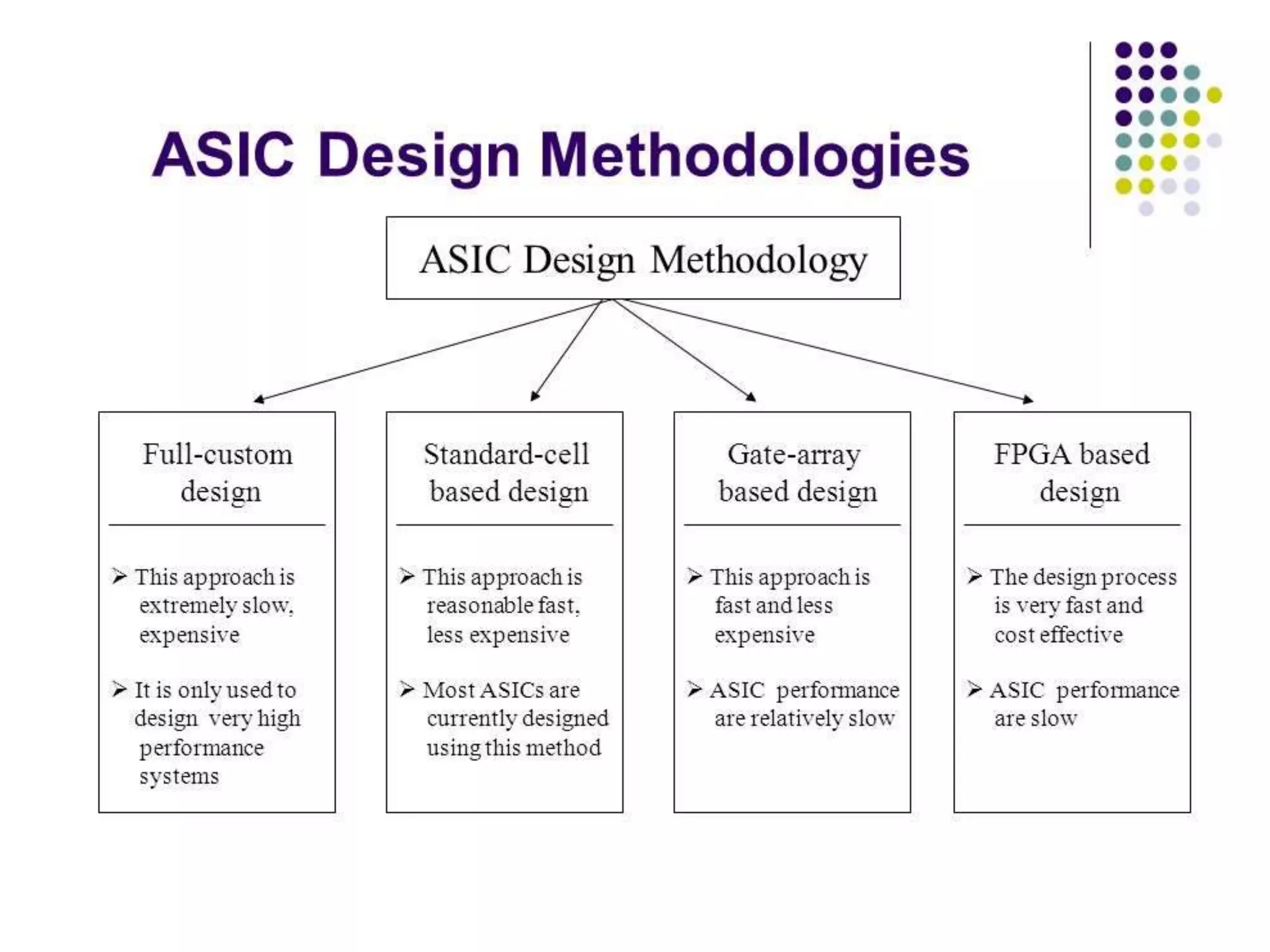
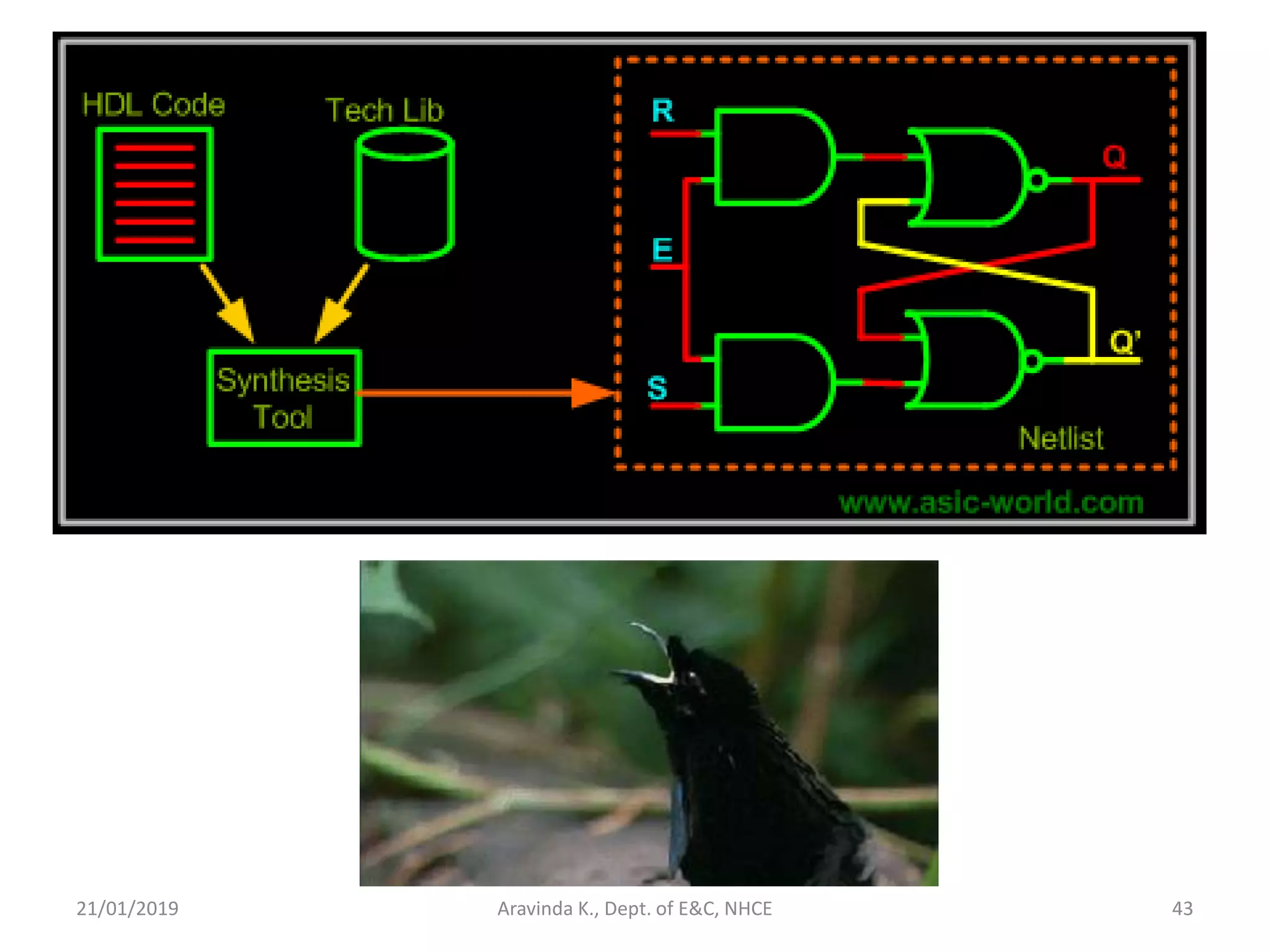
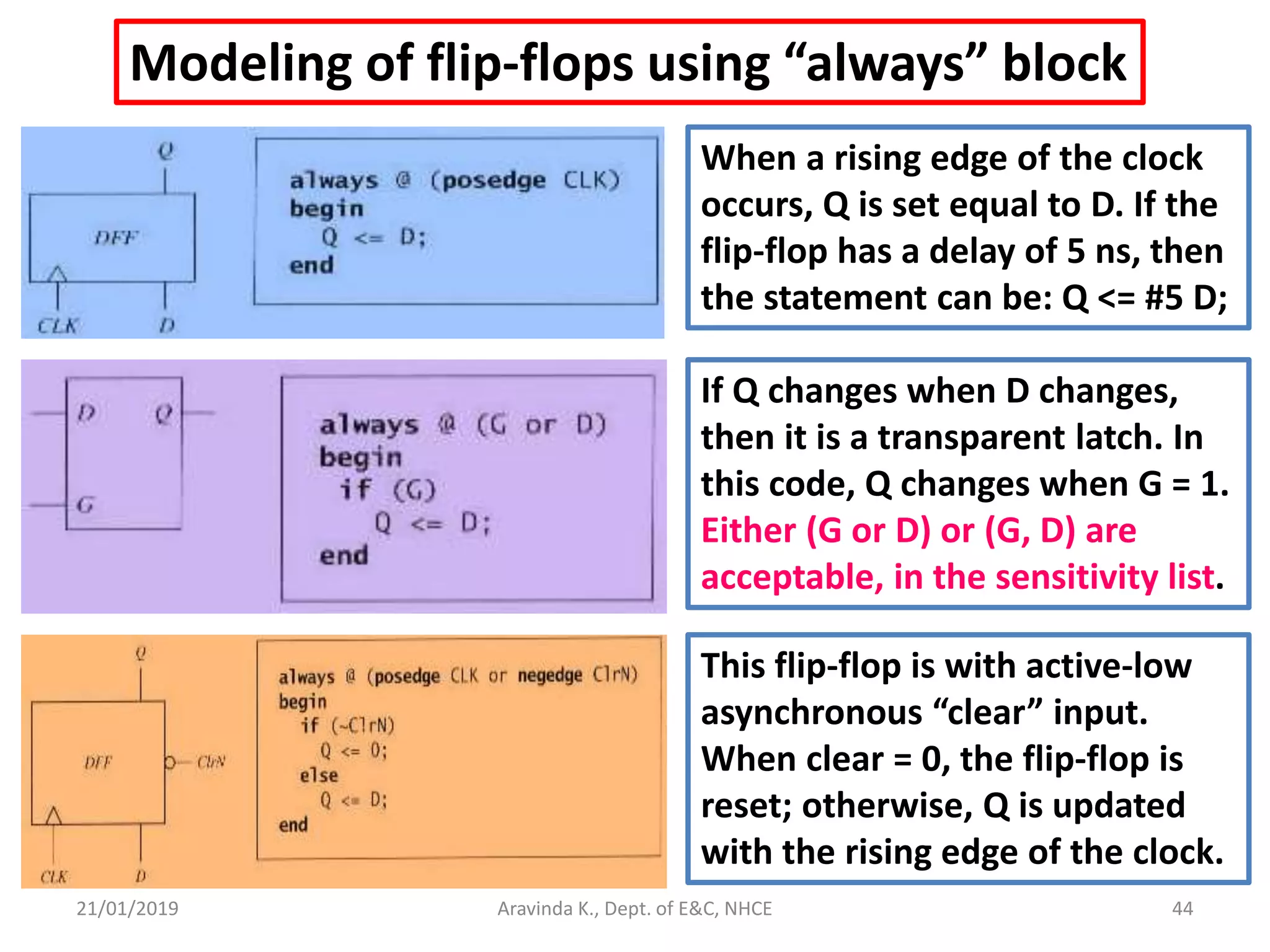
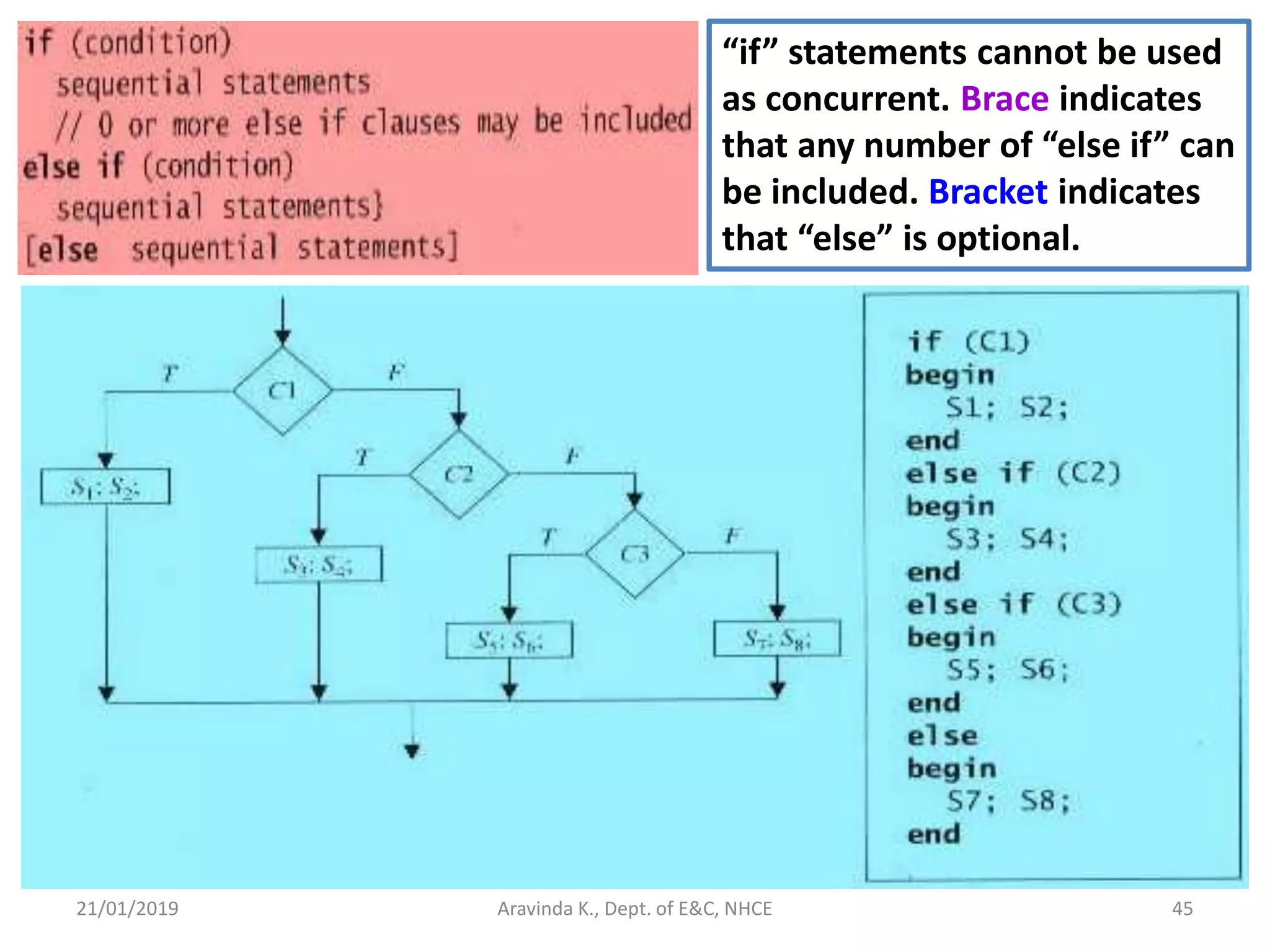
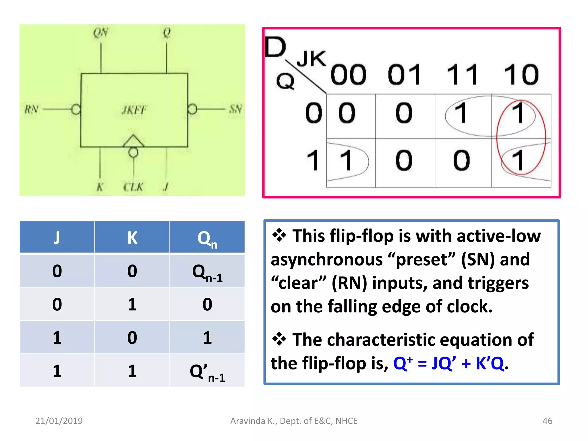
The document outlines the significance and application of Hardware Description Languages (HDLs) like Verilog in digital system design, detailing concepts such as behavioral and structural modeling, as well as synthesis processes. It emphasizes the evolution of digital circuits from SSI to ULSI and distinguishes between various targeting technologies like ASICs and FPGAs for implementation. Additionally, it covers the basic syntax and structure of Verilog, procedural assignments, and combinational logic, providing insights into the design and simulation of digital systems.