IOSR Journal of VLSI and Signal Processing (IOSR-JVSP) Volume 7, Issue 2, Ver. I (Mar. - Apr. 2017), PP 53-66 e-ISSN: 2319 – 4200, p-ISSN No. : 2319 – 4197 www.iosrjournals.org DOI: 10.9790/4200-0702015366 www.iosrjournals.org 53 | Page Design & Implementation of Subthreshold Memory Cell design based on the primary constraints T. Vasudeva Reddy1 , Dr B.K.Madhavi 2 1 Research Scholar, Dept of ECE, Rayalaseema University, Andhra Pradesh, 2 Professor, Dept of ECE, Sridevi Womens Engg College, Hyderabad, Telangana, Abstract: As there is a demand for portable electronic systems or devices, there is an incremental growth in the technology in the past few decades and also technology is cumulative at a random rate, devices are consuming large amount of power due to this the life of the battery is draining fast. so there must be a alternative devices or circuits which can reduce the power by efficiently maintaining the area and performance, therefore life of battery can be increased. As SRAM is the heart of block in all the electronic design, where the power consumption is maximum there by analyzing, estimating & modifying or changing the logic, will be able to reduce the power and performance can be greatly achieved. This proposal describes under the principle of ultra-low power logic approach which operates under subthreshold voltage operating which leads to lower power and also efficient in functionality along with secondary constraints. Index Terms: SNM, RNM, Subthreshold operation, ultra-low power applications. I. Introduction As there is demand for portable devices, Most of the electronics devices are battery operated and tremendous growth in the electronic industry, these systems are utilizing memory as their heart of the process, and will occupy maximum area and power, the amount of power that it is utilizing is maximized by a continuous operations and by lowering the technology[1]. A Digital sub threshold circuit design is a promising method for ultra-low power application, where the circuits are operating from strong inversion to moderate ,moderate to weak inversion regions. Operating these circuits in weak inversion region caused to leakage current, this new challenge in this circuits leads to innovations in the circuit design concepts. And also these circuits are operating from strong inversion to weak inversion region[2] by reducing the supply voltage up to some extend leads to, reduction in the leakage[3], and Performance characteristics voltage vs. leakage as showed below. Graph: 1 indicates the performance characteristics of voltage and leakage current.[3] SRAM is heart of the core processing unit and changing the performance characteristics from write to read and read to write with on chip solutions, for high performance and more reliable applications, there by changing the parameters with power, therefore the energy consumed per bit is reduced[4], which will makes the more efficient design. in order to change the the power consumption of SRAM ,there is dependency on different types of process variations of the cell topology like sensing unit, supply voltage. This paper represents SRM is designed model staring from 6T SRAM vs different parameters & characteristics, power consumption[5] for each operation of write and read ,temperature, sizing of each cell and also knowing the advantages & dis advantages of each model 8t 9t,10t, over a functionality. This Paper described as follows section II explain about operation of 6T SRAM read and write operation, and its characteristics. section III explains Limitation of 6t cell and how to improve performance. comparison and analysis of SRAM models 6T,8T,9T,10T different configuration is made and estimating the characteristics, in section IV accommodation of different models of SRAM and its comparisons in different aspects, in section V Improvement of 8t SRAM by an advanced approach and making a comparison with the
Design & Implementation of Subthreshold Memory Cell design based on the primary constraints DOI: 10.9790/4200-0702015366 www.iosrjournals.org 54 | Page existing 8T SRAM.with the above mentioned parameters, in the next section VI, describes the advanced 8t SRAM is replaced with Source coupled logic, of variable threshold and estimating the different parameters, section VII concludes the efficiency of Transistor logic with all the parameters. and also enhancements and future scope. II. SRAM Cell Operation & Performance Characterstics The number of techniques that were proposed in the past few decades for the systems to operate in the subthreshold operation under ultra-low power applications to reduce the supply voltage lesser than threshold voltage, therefore the substantial leakage gate current is reduced especially in nanometer technology.The current that is dissipated during the components under inactive state. And the threshold leakage currents were proposed [6,14]. The challenges of subthreshold memory design and a dense, low energy 6-T cell that effectively combats variability. First deep subthreshold 6-T SRAM design were proposed [5] that provides accurate estimation of the effects of process variations balance that is useful for understanding the impact of process variations as it is a bi stable latch. Different types of SRAM bit cells have been proposed to improve the memory failure probability at a given supply voltage. Fig 1: 6T SRAM Cell with A Word Line And Data Input And Output III. 6t Sram Cell Operation 6T cells utilize differential write/Read operation, write operation will be performed whenever a change in the transition on the inputs, during this wl is high and output is complementary to the input. Read operation will be performed when there is no change in the transition of the input with WL is high [5]. A sense amplifier converts the differential signal to a logic-level output. Then, at the end of the read cycle, the BLs returns to the positive supply rail. During write,VWL is raised and the BLs are forced to either VDD (depending on the data), overpowering the contents of the memory cell. During hold, VWL is held low and the BLs are left floating or driven to VDD. 6T SRAM cell: Fig 2: schematic representation of 6T SRAM SRAM implementation represents in fig 2 of 6T bit cell of 6T, used with High Vth nMOS transistors for reducing the Leakage Power [1]. The ratios of nMOS and pMOS are maintained with design considerations. To drive transistors (M1,M4) should be stronger enough to access the Access transistors (M2,M5) to minimize the disturbance in Read Mode. and in the Write Mode, Access transistors should be strong enough to operate (M3,M6) for successful write operation. And Characteristics of 6T SRAM is represented as showed below
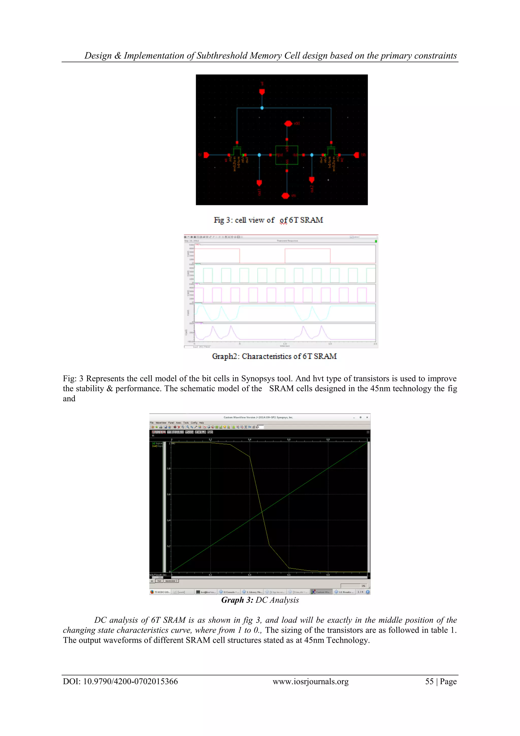
Design & Implementation of Subthreshold Memory Cell design based on the primary constraints DOI: 10.9790/4200-0702015366 www.iosrjournals.org 55 | Page Fig: 3 Represents the cell model of the bit cells in Synopsys tool. And hvt type of transistors is used to improve the stability & performance. The schematic model of the SRAM cells designed in the 45nm technology the fig and Graph 3: DC Analysis DC analysis of 6T SRAM is as shown in fig 3, and load will be exactly in the middle position of the changing state characteristics curve, where from 1 to 0., The sizing of the transistors are as followed in table 1. The output waveforms of different SRAM cell structures stated as at 45nm Technology.
Design & Implementation of Subthreshold Memory Cell design based on the primary constraints DOI: 10.9790/4200-0702015366 www.iosrjournals.org 56 | Page Table 1: Transistor sizing of the 6T SRAM cell The limitation in 6T RAM is static Noise Margin [12]as showed in the graph 4..there should be maximum static noise margin between the read and write operation, when changing the states from write to read. Graph4 : Static Noise Margin of 6T SRAM cell write operation when a logic and WL is high a data will be stored into SRAM, for a clock cycle ,and when the logic the data will be remains in the output, once the logic is changed, data in the output will be shifted to another logic. IV. 8t Sram Cell Two transistors were added to the 6T SRAM, read and write operations of Performance can be completely separated. A separate read stack is controlled by a Read Word Line (RWL). The remaining 6T portion of the cell is optimized [7] for writing operation, resulting in overall lower Vmin voltage.A Separated data retention element and data output element means that there will be no correlation between the read SNM Cell and l. Thus, an 8TSRAM design [7] contains a write assist in which a horizontally routed VDD line is collapsed as showed in the fig 4. Fig 4: 8T Subthreshold SRAM Cell Fig 5: 8T schematic model of SRAM Cell
Design & Implementation of Subthreshold Memory Cell design based on the primary constraints DOI: 10.9790/4200-0702015366 www.iosrjournals.org 57 | Page The Fig.5 shows that 8T SRAM bit cell is designed with two sleep mode transistors, connected as pull down mode transistors [7] to achieve low power design mode and to avoid the static noise margin. To write data '1' into SRAM cell the WL is asserted and BL is made high and BLB is low. To write '0' BL is low and BLB keeping high. The values of '0' or '1' can be stored at node Q and its complement at node QB. Reading the stored value at node “Q” by precharging operation. After precharging the Bit Lines (BL=BLB=1) asserting the WL and pulling down the one of the Bit Line low [8]. Data stability is increased with 8T. 9T SRAM Cell The Fig.5a.demonstrates that 9T SRAM bit cell is to not only to reduce the leakage power also to enhance data stability. The upper sub-circuit of the memory cell is essentially same as 6T SRAM cell. The two write access transistors (M2, M5) are controlled by a write signal (WL). The lower sub-circuit of the cell is composed of the bit line and access transistors (M7,M8), the read access transistor (M9). Operation of M7 and M8 are controlled by the data stored in the cell. M9 is controlled by a separate read signal (RD) [5a.]in write operation WL is asserted and making High and Read signal RD is maintained low. Transistors (M2,M5) are turned ON. Then the data can be stored at node Q. and this data can be Read by asserting read signal RD to high and WL to low. problem n 8T is indicated by occupying larger area and static noise margin is improved.[8][13]. The schematic diagram of the 9T SRAM cell, for CMOS technology, is shown in Fig.9. The upper sub circuit of the 9T memory circuit is essentially a 6T SRAM cell with minimum sized devices(composed of M3, M4, M5, M6, M1 and M2).The two write access transistors (M5 and M6) are controlled by a write signal ie word line (WL). The data is stored within this upper memory sub-circuit. The lower sub circuit of the new cell is composed of the bit-line access transistors (M7 and M8) and the read access transistor (M9). The operations of M7 and M8 are controlled by the data stored in the cell. M9 is controlled by a separate read signal (RD) [8][17].The 9T SRAM cell completely isolates the data from the bit lines during a read operation. Fig.5a. 9T SRAM sub threshold Circuit Table: 2 sizing of 9T SRAM The length and widths of the 9T is as showed in the below table. Where the length is constant and width is changing based on the ids and vds relationship[11]. Fig10: Schematic diagram of 9T SRAM cell
Design & Implementation of Subthreshold Memory Cell design based on the primary constraints DOI: 10.9790/4200-0702015366 www.iosrjournals.org 58 | Page Graph: 5. 9T SRAM characteristics at 400 mv 10 T SRAM Cell: Fig.7. shows the schematic model of the 10T SRAM sub threshold logic cell[7][10]. Transistors are equal to a 6T cell except the source of M1 and M2 tie to a virtual supply voltage rail of Vdd. Write admission to the bit cell happens through the write contact transistors M5 and M6, Transistors from the write Bit lines, WBLT and WBLC. Transistors M8 through M10 implement a buffer used for reading. Fig.7. circuit diagram of the 10T SRAM cell. Read access is a single-ended occurs on a separate bit line RBL, which is pre-charge to read access. The word line read word line is also distinct from the write word line. One key Advantage is to separating the read & write word lines and bit lines is that a memory using bit cell can have distinct read and write ports across the circuit. And schematic model is as showed in fig 8. Fig.8: schematic diagram of 10 TSRAM Table: 3 Transistor sizing of the 10T SRAM cell Represents the sizes of length and widths of the Transistors Configd as mentioned above
Design & Implementation of Subthreshold Memory Cell design based on the primary constraints DOI: 10.9790/4200-0702015366 www.iosrjournals.org 59 | Page Graph 4: Characteristics of 10T SRAM chcterstics are as shaowned above and are represented with read and write lines Vii A. Effect Of Temperature On Leakage Power And Current On Sram Bit Cells All the circuits have been simulated using 45nm technology on Synopsys tool with supply voltage of different ranging [15]. To make the neutral testing environment all the circuits has been simulated with the same input patterns. Graph 7. Leakage current variation of SRAM cell with Temperature Characteristics of 7 and 8 shows comparative analysis of the circuits stated above at 45nm. The simulation results reveal that 8T SRAM Cell at 45nm technology shows always best performance for the range of power consumption, operating frequency and temperature Fig .15 Leakage power variations of SRAM cells with Temperature The leakage power and current of the SRAM cells for every 10 degrees rise or fall in temperature about 6-7% for 6T SRAM cell and 8T SRAM has 1-2% of current leakage and 0.1% of power leakage which shows that 8T will be the better one amongst the other SRAM cells[15]. The power dissipation reduction in SRAMs is not only due to power supply voltage reduction, but also to operating frequency and temperature. All the above figs depicts that SRAM cells at 45nm technology and 8T SRAM cell at 45nm technology shows better performance for the range of frequency and temperature among all the other design approaches[19] for SRAM cell. This paper tries to find out an efficient SRAM memory cell in both the aspects power consumption and speed in terms of power delay product at different technologies[16]. The above table gives us a comparative study of the bit cells based on leakage and temperature at room temperature i.e.,27degrees at the subthreshold voltage operation B. Performance Metrics Of Power Consumption For Read And Write Operation, Leakage Power And Delay At 90 Nm These simulation results indicate the different SRAM bit cells. Analysis of different parameters of power consumption, leakage power and delay under the sub threshold region. Measurements have been observed over the of voltages from 0.8V down to the sub threshold region at 90 nm and 45 nm technologies. Comparison of all the bit cells for parameters have been shown with respect to technologies.In 90nm technology the parameters like power consumption, leakage power and delay are shown below (Fig9 to Fig13) power consumption and
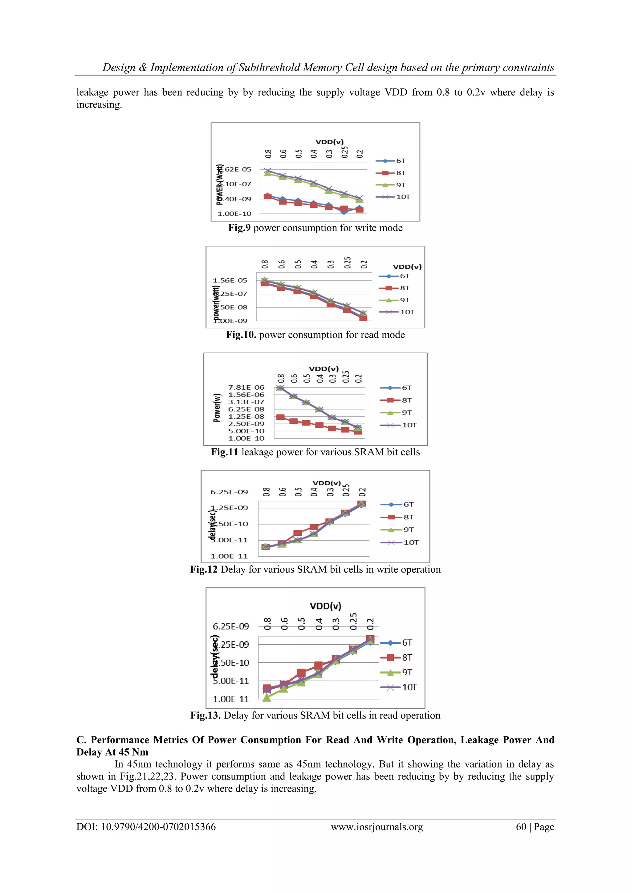
Design & Implementation of Subthreshold Memory Cell design based on the primary constraints DOI: 10.9790/4200-0702015366 www.iosrjournals.org 60 | Page leakage power has been reducing by by reducing the supply voltage VDD from 0.8 to 0.2v where delay is increasing. Fig.9 power consumption for write mode Fig.10. power consumption for read mode Fig.11 leakage power for various SRAM bit cells Fig.12 Delay for various SRAM bit cells in write operation Fig.13. Delay for various SRAM bit cells in read operation C. Performance Metrics Of Power Consumption For Read And Write Operation, Leakage Power And Delay At 45 Nm In 45nm technology it performs same as 45nm technology. But it showing the variation in delay as shown in Fig.21,22,23. Power consumption and leakage power has been reducing by by reducing the supply voltage VDD from 0.8 to 0.2v where delay is increasing.
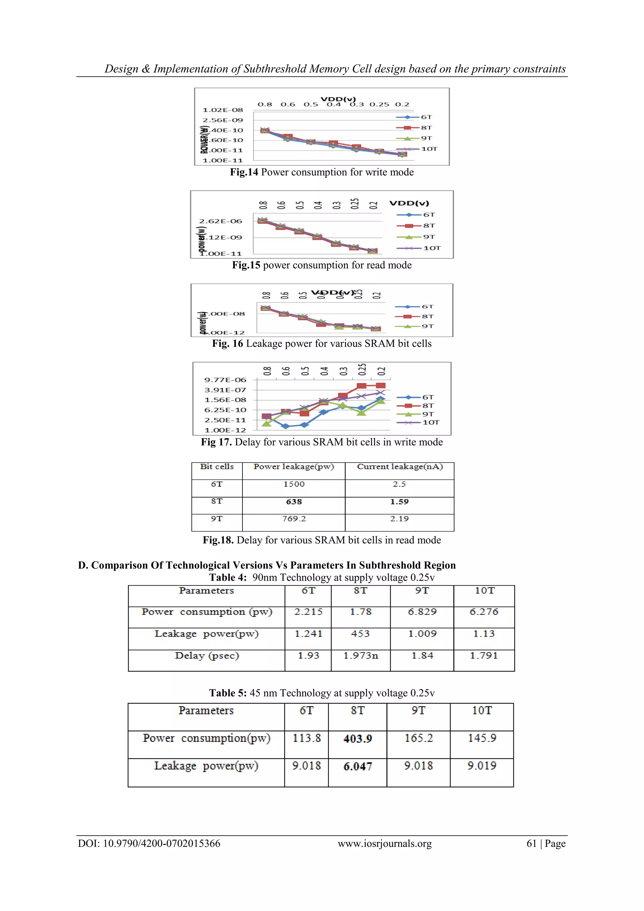
Design & Implementation of Subthreshold Memory Cell design based on the primary constraints DOI: 10.9790/4200-0702015366 www.iosrjournals.org 61 | Page Fig.14 Power consumption for write mode Fig.15 power consumption for read mode Fig. 16 Leakage power for various SRAM bit cells Fig 17. Delay for various SRAM bit cells in write mode Fig.18. Delay for various SRAM bit cells in read mode D. Comparison Of Technological Versions Vs Parameters In Subthreshold Region Table 4: 90nm Technology at supply voltage 0.25v Table 5: 45 nm Technology at supply voltage 0.25v
Design & Implementation of Subthreshold Memory Cell design based on the primary constraints DOI: 10.9790/4200-0702015366 www.iosrjournals.org 62 | Page Table 6: Comparative results of power and leakage current with different transistors of SRAM. The paper indicates the comparative results of power consumption; leakage power and delay for both read and write modes of operations in various technologies such as 90nm and 45nm of various SRAM Bit cells. It has been observed that the leakage power is reduced by a factor 43% and 25% in consumption in 90 nm technology, But in 45nm technology power consumption is reduced by a factor of 45 % and leakage power is reduced by a factor of 21%. Delay is reduced in 9T SRAM Bit cell than the 6T/8T SRAM Bit cell. In subthreshold region it is observed that the standard SRAM bit cell performance is given less priority than 8T and 9T SRAM bit cells. The leakage power is reduced by using the high Vth nMOS transistors. Power dissipation reduction in SRAMs is not only due to supply voltage, but also depends on the operating frequency[22] and room temperature. All the above figs portray that SRAM cells at 45nm technology shows better performance over a frequency and temperature among all the other design approaches. This paper found out an efficient SRAM memory cell in both the aspects power consumption and speed in terms of power delay product at different technologies. The above table gives us a comparative study of the bit cells based on leakage at room temperature i.e., 27degrees at the subthreshold voltage operation Proposed Sram Architecture Schmitt Trigger-Based Sub-Vt 8T Static Ram Using 45 nm By Bit Interleaving Method SRAM is a type of volatile semiconductor memory to store binary logic '1' and '0' bits. It uses bi stable latch circuitry made of Transistors/MOSFETS to store each bit. An SRAM is designed to fill two needs to provide a direct interface with the CPU at speeds not attainable by DRAMs and to replace DRAMs in systems that require very low power consumption. The design requirement is such that PMOS OFF-state current should be more than the pull-down nMOS transistor leakage current for maintaining data “1” reliably. With increasing process variations and exponential dependence of the sub-threshold current on the threshold voltage, satisfying this design requirement across different process, voltage, and temperature (PVT) conditions may be challenging.[13] Proposed Architecture is designed using Schmitt trigger-based 8T SRAM bit cell illustrated in Fig.[7]. It is similar to the standard 6T SRAM cell, however it is used High-Vth nMOS in this design [7]. Two sleep transistors are used in pull down path to minimize the leakage power [15]. These Transistors used for self- correcting feedback to achieve stable operation. This cell also reduces dynamic power in active mode. A. Schmitt Trigger-Based 8t Sram nMOS should win the ratio fight with pMOS. If we want to write data'1' making the WL=1 and one of the bit line keeping High BL(or)BLB=1 and other is 0.Then the value is been written as '1' at node 'Q' and its complement at node 'QB'. B. Write Operation In the write operation, WL is enabled to activate the access transistors for data transfer . The proper write operation can be done successfully by consideration of ratio(W/L) of nMOS and pMOS[8]. In sizing of transistors in SRAM bit cell. Fig.9. The Schematic of a single cell write operation
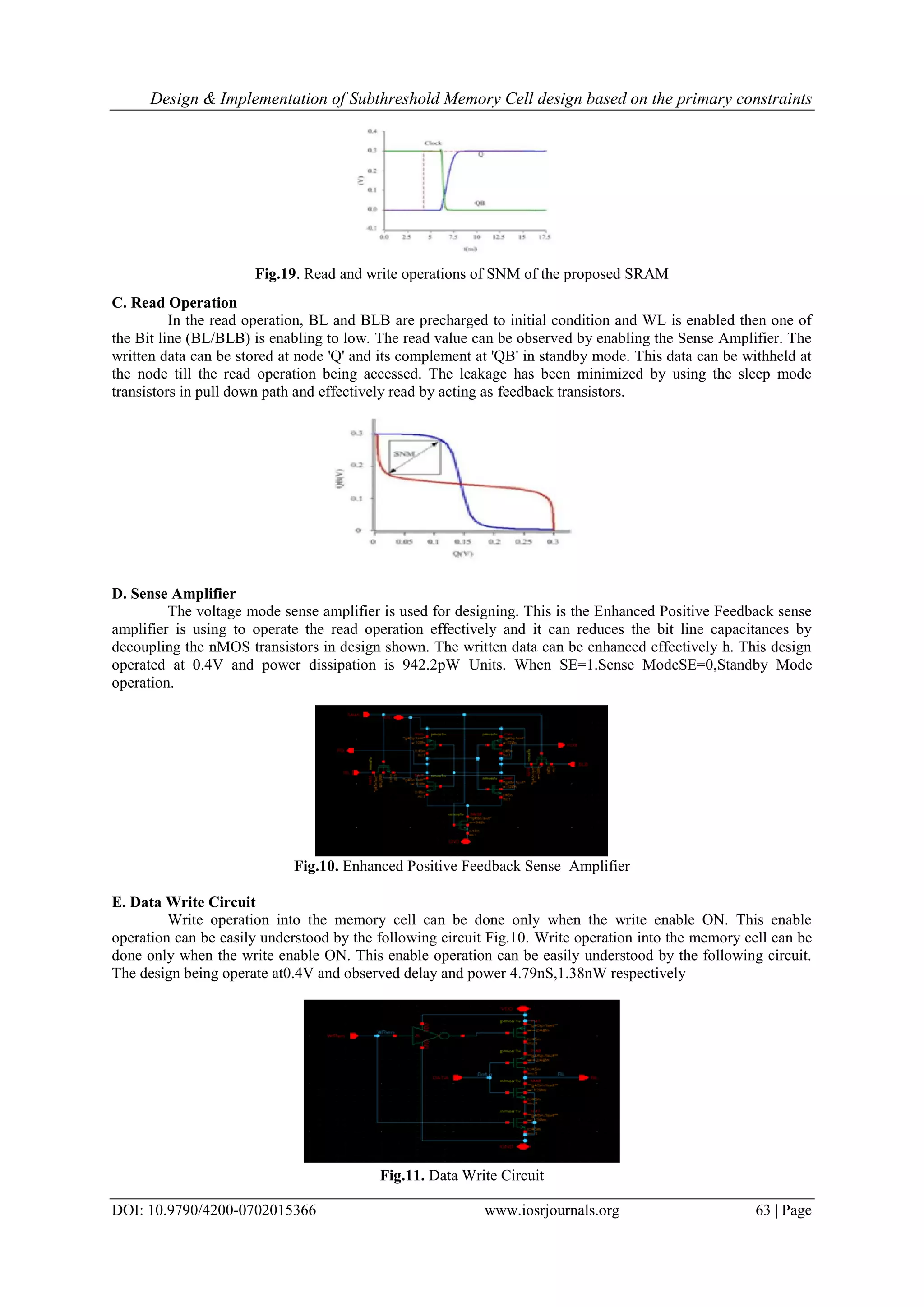
Design & Implementation of Subthreshold Memory Cell design based on the primary constraints DOI: 10.9790/4200-0702015366 www.iosrjournals.org 63 | Page Fig.19. Read and write operations of SNM of the proposed SRAM C. Read Operation In the read operation, BL and BLB are precharged to initial condition and WL is enabled then one of the Bit line (BL/BLB) is enabling to low. The read value can be observed by enabling the Sense Amplifier. The written data can be stored at node 'Q' and its complement at 'QB' in standby mode. This data can be withheld at the node till the read operation being accessed. The leakage has been minimized by using the sleep mode transistors in pull down path and effectively read by acting as feedback transistors. D. Sense Amplifier The voltage mode sense amplifier is used for designing. This is the Enhanced Positive Feedback sense amplifier is using to operate the read operation effectively and it can reduces the bit line capacitances by decoupling the nMOS transistors in design shown. The written data can be enhanced effectively h. This design operated at 0.4V and power dissipation is 942.2pW Units. When SE=1.Sense ModeSE=0,Standby Mode operation. Fig.10. Enhanced Positive Feedback Sense Amplifier E. Data Write Circuit Write operation into the memory cell can be done only when the write enable ON. This enable operation can be easily understood by the following circuit Fig.10. Write operation into the memory cell can be done only when the write enable ON. This enable operation can be easily understood by the following circuit. The design being operate at0.4V and observed delay and power 4.79nS,1.38nW respectively Fig.11. Data Write Circuit
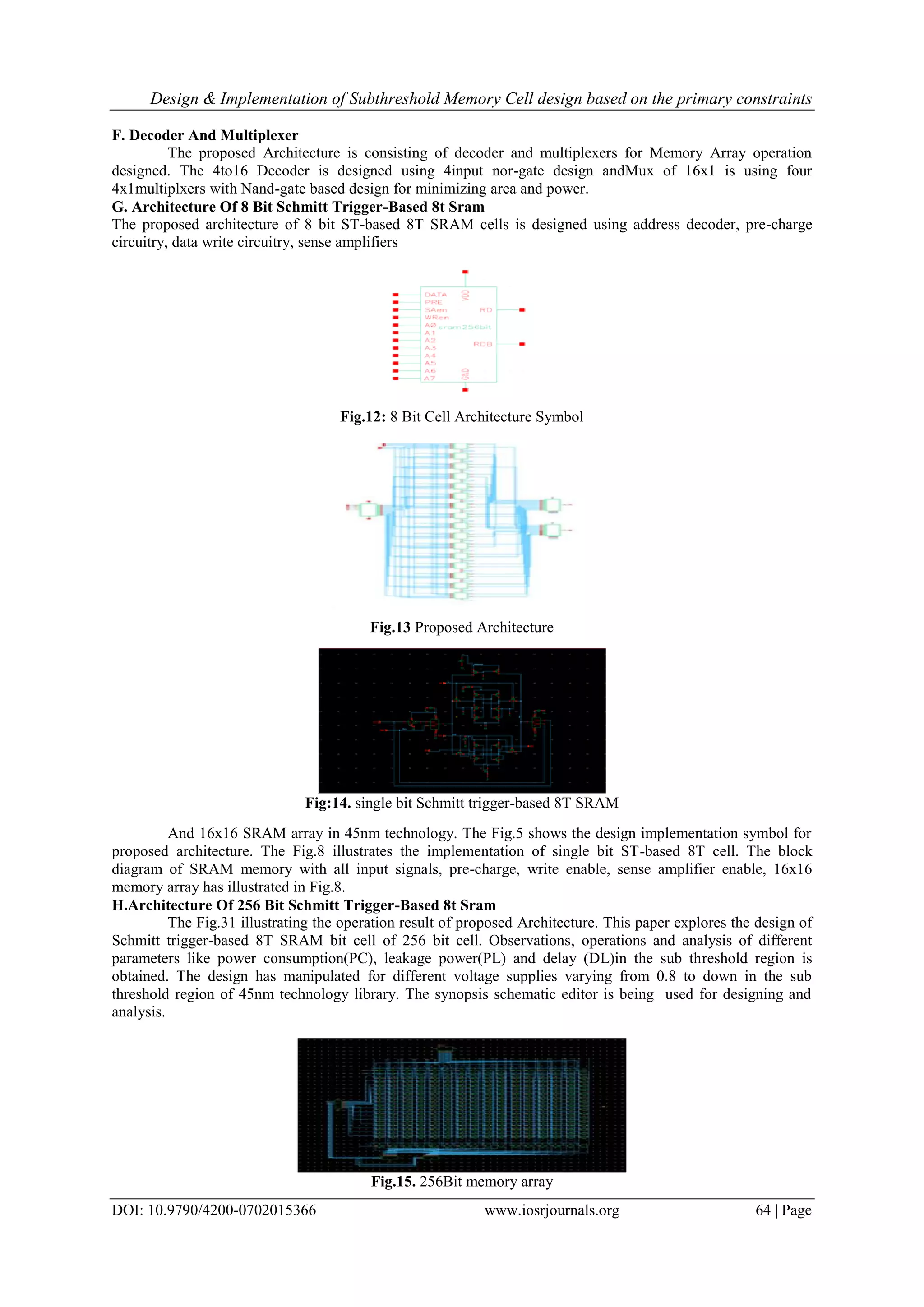
Design & Implementation of Subthreshold Memory Cell design based on the primary constraints DOI: 10.9790/4200-0702015366 www.iosrjournals.org 64 | Page F. Decoder And Multiplexer The proposed Architecture is consisting of decoder and multiplexers for Memory Array operation designed. The 4to16 Decoder is designed using 4input nor-gate design andMux of 16x1 is using four 4x1multiplxers with Nand-gate based design for minimizing area and power. G. Architecture Of 8 Bit Schmitt Trigger-Based 8t Sram The proposed architecture of 8 bit ST-based 8T SRAM cells is designed using address decoder, pre-charge circuitry, data write circuitry, sense amplifiers Fig.12: 8 Bit Cell Architecture Symbol Fig.13 Proposed Architecture Fig:14. single bit Schmitt trigger-based 8T SRAM And 16x16 SRAM array in 45nm technology. The Fig.5 shows the design implementation symbol for proposed architecture. The Fig.8 illustrates the implementation of single bit ST-based 8T cell. The block diagram of SRAM memory with all input signals, pre-charge, write enable, sense amplifier enable, 16x16 memory array has illustrated in Fig.8. H.Architecture Of 256 Bit Schmitt Trigger-Based 8t Sram The Fig.31 illustrating the operation result of proposed Architecture. This paper explores the design of Schmitt trigger-based 8T SRAM bit cell of 256 bit cell. Observations, operations and analysis of different parameters like power consumption(PC), leakage power(PL) and delay (DL)in the sub threshold region is obtained. The design has manipulated for different voltage supplies varying from 0.8 to down in the sub threshold region of 45nm technology library. The synopsis schematic editor is being used for designing and analysis. Fig.15. 256Bit memory array
Design & Implementation of Subthreshold Memory Cell design based on the primary constraints DOI: 10.9790/4200-0702015366 www.iosrjournals.org 65 | Page Table.7: operation result of SRAM Cell VDD Single bit 16bit 256bit Power Consumption(PW) 12.765nW 317.9nW 474.6nW Leakage Power(PL) 0.497nW 4.74nW 7.98nW Delay 114.6ns 156.4ns 168.9ns Fig.21. Performance characteristics of operation V. Conclusion The paper gives a broad idea about designing of memory cell using number of transistors with different technologies and operating at different subthreshold regions, and has been shown that the comparative results of power consumption(PC), leakage power(PL) and delay (DL)for both read and write modes of operations in various technologies such as 90nm various SRAM Bit cells. Its has observed that the leakage power is reduced by a factor 43% and 25% in consumption in 90 nm technology using 8T transistor modeling. And in 45nm Technology power consumption is reduced by a factor of 45 % and leakage power is reduced by a factor of 21%. Delay is reduced in 9T SRAM Bit cell than 6T/8T SRAM bit cell. But in subthreshold region it is observed that the standard SRAM bit cell performance is given less priority than 8T and 9T SRAM bit cells. The leakage power is reduced by using the high Vth nMOS transistors. References [1] SRAM cell with improved stability and reduced leakage current for subthreshold region of operation” by P. Sreelakshmi, K. S. Pande and N. S. Murty In 2015 IEEE International Conference on Computational Intelligence and Computing Research (ICCIC), Madurai, 2015, pp. 1-5.doi: 10.1109/ICCIC.2015.7435750. [2] David J. Comer, Senior Member, IEEE, and Donald T. Comer"Operation of Analog MOS Circuits in the Weak or Moderate Inversion Region" IEEE TRANSACTIONS ON EDUCATION, VOL. 47, NO. 4, NOVEMBER 2004. [3]. "Low-power 9T subthreshold SRAM cell with single-ended write scheme, By A. Sinha, V. Kumar and A. Islam, " 2015 AnnualIEEE India Conference (INDICON), New Delhi, 2015, pp. 1-6.doi: 10.1109/INDICON.2015.7443137.[10]. "Analysis of SRAM cell designs for low power applications, By C. K. Sharma and R. Chandel, " Convergence of Technology (I2CT), 2014 International Conference for, Pune, 2014, pp. 1-4.doi: 10.1109/I2CT.2014.7092157 [3] Alice Wang Benton H. Calhoun Anantha P. Chandrakasan "Sub-threshold Design for Ultra Low-Power Systems"SERIES ON INTEGRATED CIRCUITS AND SYSTEMS [4] Chang, L. Montoye, R.K. Nakamura, Y.Batson, K.A.Eickemeyer, R.J.Dennard, R.H. Haensch,W.Jamsek, D, “An 8T-SRAM for variability tolerance and low-voltage operation in highperformancecaches”, Solid-State Circuits, IEEE Journal vol. 43, April 2008, Issue 4, pp-956-963. [5] NavidAzizi, FaridN.Najm. An asymmetricSRAM cell to lower gate leakage. In proceedingsof International Symposium on Quality ElectronicDesign, pp.534-539, March 2004 [6] Ravi Kumar. K. I, Vijayalaxmi. C. Kalal, Rajani. H. P, Dr. S. Y. Kulkarni"Design and Verification of Low Power 64bit SRAM System using 8T SRAM:Back-End Approach" International Journal of Engineering and Innovative Technology (IJEIT) Volume 1, Issue 6, June 2012. [7] A new low-leakage T-Gate based 8T SRAM cell with improved write-ability in 90nm CMOS technology, G. Pasandi, E. Qasemi and S. M. Fakhraie, " 2014 22nd Iranian Conference on Electrical Engineering (ICEE), Tehran,2014,pp.382-386.doi- 10.1109/IranianCEE.2014.6999569 [8] Chang, L. Montoye, R.K. Nakamura, Y.Batson, K.A.Eickemeyer, R.J.Dennard, R.H. Haensch,W.Jamsek, D, “An 8T-SRAM for variability tolerance and low-voltage operation in highperformancecaches”, Solid-State Circuits, IEEE Journal vol. 43, April 2008, Issue 4, pp-956-963. [9] Wei-Bin Yang, Chi-Hsiung Wang, I-Ting Chuo, Huang- Hsuan Hsu" A 300 mV 10 MHz 4 kb10T Subthreshold SRAM for Ultralow-Power Application" 2012 IEEE International Symposium on Intelligent Signal Processing and Communication Systems (ISPACS 2012) November 4-7, 2012. [10] Zhiyu Liu and Volkan Kursun "Characterization of a Novel Nine-Transistor sram cell" ieee transactions on very large scale integration (vlsi) systems, vol. 16, no. 4, april 2008 [11] Koichi Takeda , “A read static noise margin free SRAM cell for low Vdd and high speed applications”, Solid-State Circuits, IEEE Journal vol. 41, Jan.2006, Issue 1, pp.113-121. [12] Zhiyu Liu, Volkan Kursun, “ Characterization of a novel nine transistor SRAM cell”, IEEE Transactions on Very Large Scale Integration Systems,vol.46, Issue 4,April 2008.pp-488-492.
Design & Implementation of Subthreshold Memory Cell design based on the primary constraints DOI: 10.9790/4200-0702015366 www.iosrjournals.org 66 | Page [13] A Feasibility Study of Subthreshold SRAM Across Technology Generations” ArijitRaychowdhury, SaibalMukhopadhyay, and Kaushik Roy Dept. of ECE, Purdue University, West Lafayette, IN-47907 <araycho, sm, kaushik>@ecn.purdue.edu. [14] Jawar Singh, DhirajK.Pradhan,” A single ended 6T SRAM cell design for ultra low voltageapplications”, IEICE Electronic Express, 2008, pp-750-755. [15] "Analysis of SRAM cell designs for low power applications," by C. K. Sharma and R. Chandel, Convergence of Technology (I2CT), 2014 International Conference for, Pune, 2014, pp. 1-4.doi: 10.1109/I2CT.2014.7092157 [16] A 1kb 9T subthreshold SRAM with bit-interleaving scheme in 65nm CMOS BY M. H. Chang, Y. T. Chiu, S. L. Lai and W. Hwang, Low Power Electronics and Design (ISLPED) 2011 International Symposium on, Fukuoka, 2011, pp. 291-296.doi: 10.1109/ISLPED.2011.5993652 [17] B. Zhai, et al., “Analysis and Mitigation of Variability in Subthreshold Design,” ISLPED, pp. 20-25, 2005. [18] “Analyzing and Modeling Process Balance for Sub-threshold Circuit Design” Joseph F. Ryan, Jiajing Wang, and Benton H. Calhoun Department of Electrical and Computer Engineering University of Virginia, Charlottesville, Virginia 22904 [19] A. Wang, B. Calhoun, and A. Chandrakasan, “Sub-threshold Design for Ultra Low-Power Systems”, Springer, 2006.[15] “A 160 mV Robust Schmitt Trigger Based Subthreshold SRAM” Jaydeep P. Kulkarni, Student Member, IEEE, Keejong Kim, and Kaushik Roy, Fellow, IEEE. [20] H.Soeleman and K. Roy,” Ultra-low power digital subthreshold logic circuits,” International Symposium on Low Power Electronics and Design (ISLPED 99), pp. 94–96, San Diego, California, USA, July 1999. [21] “An Ultra-Low-Power Memory With a Subthreshold Power Supply Voltage” Jinhui Chen, Student Member, IEEE, Lawrence T. Clark, Senior Member, IEEE, and Tai-Hua Chen, Student Member, IEEE

Design & Implementation of Subthreshold Memory Cell design based on the primary constraints

  • 1.
    IOSR Journal ofVLSI and Signal Processing (IOSR-JVSP) Volume 7, Issue 2, Ver. I (Mar. - Apr. 2017), PP 53-66 e-ISSN: 2319 – 4200, p-ISSN No. : 2319 – 4197 www.iosrjournals.org DOI: 10.9790/4200-0702015366 www.iosrjournals.org 53 | Page Design & Implementation of Subthreshold Memory Cell design based on the primary constraints T. Vasudeva Reddy1 , Dr B.K.Madhavi 2 1 Research Scholar, Dept of ECE, Rayalaseema University, Andhra Pradesh, 2 Professor, Dept of ECE, Sridevi Womens Engg College, Hyderabad, Telangana, Abstract: As there is a demand for portable electronic systems or devices, there is an incremental growth in the technology in the past few decades and also technology is cumulative at a random rate, devices are consuming large amount of power due to this the life of the battery is draining fast. so there must be a alternative devices or circuits which can reduce the power by efficiently maintaining the area and performance, therefore life of battery can be increased. As SRAM is the heart of block in all the electronic design, where the power consumption is maximum there by analyzing, estimating & modifying or changing the logic, will be able to reduce the power and performance can be greatly achieved. This proposal describes under the principle of ultra-low power logic approach which operates under subthreshold voltage operating which leads to lower power and also efficient in functionality along with secondary constraints. Index Terms: SNM, RNM, Subthreshold operation, ultra-low power applications. I. Introduction As there is demand for portable devices, Most of the electronics devices are battery operated and tremendous growth in the electronic industry, these systems are utilizing memory as their heart of the process, and will occupy maximum area and power, the amount of power that it is utilizing is maximized by a continuous operations and by lowering the technology[1]. A Digital sub threshold circuit design is a promising method for ultra-low power application, where the circuits are operating from strong inversion to moderate ,moderate to weak inversion regions. Operating these circuits in weak inversion region caused to leakage current, this new challenge in this circuits leads to innovations in the circuit design concepts. And also these circuits are operating from strong inversion to weak inversion region[2] by reducing the supply voltage up to some extend leads to, reduction in the leakage[3], and Performance characteristics voltage vs. leakage as showed below. Graph: 1 indicates the performance characteristics of voltage and leakage current.[3] SRAM is heart of the core processing unit and changing the performance characteristics from write to read and read to write with on chip solutions, for high performance and more reliable applications, there by changing the parameters with power, therefore the energy consumed per bit is reduced[4], which will makes the more efficient design. in order to change the the power consumption of SRAM ,there is dependency on different types of process variations of the cell topology like sensing unit, supply voltage. This paper represents SRM is designed model staring from 6T SRAM vs different parameters & characteristics, power consumption[5] for each operation of write and read ,temperature, sizing of each cell and also knowing the advantages & dis advantages of each model 8t 9t,10t, over a functionality. This Paper described as follows section II explain about operation of 6T SRAM read and write operation, and its characteristics. section III explains Limitation of 6t cell and how to improve performance. comparison and analysis of SRAM models 6T,8T,9T,10T different configuration is made and estimating the characteristics, in section IV accommodation of different models of SRAM and its comparisons in different aspects, in section V Improvement of 8t SRAM by an advanced approach and making a comparison with the
  • 2.
    Design & Implementationof Subthreshold Memory Cell design based on the primary constraints DOI: 10.9790/4200-0702015366 www.iosrjournals.org 54 | Page existing 8T SRAM.with the above mentioned parameters, in the next section VI, describes the advanced 8t SRAM is replaced with Source coupled logic, of variable threshold and estimating the different parameters, section VII concludes the efficiency of Transistor logic with all the parameters. and also enhancements and future scope. II. SRAM Cell Operation & Performance Characterstics The number of techniques that were proposed in the past few decades for the systems to operate in the subthreshold operation under ultra-low power applications to reduce the supply voltage lesser than threshold voltage, therefore the substantial leakage gate current is reduced especially in nanometer technology.The current that is dissipated during the components under inactive state. And the threshold leakage currents were proposed [6,14]. The challenges of subthreshold memory design and a dense, low energy 6-T cell that effectively combats variability. First deep subthreshold 6-T SRAM design were proposed [5] that provides accurate estimation of the effects of process variations balance that is useful for understanding the impact of process variations as it is a bi stable latch. Different types of SRAM bit cells have been proposed to improve the memory failure probability at a given supply voltage. Fig 1: 6T SRAM Cell with A Word Line And Data Input And Output III. 6t Sram Cell Operation 6T cells utilize differential write/Read operation, write operation will be performed whenever a change in the transition on the inputs, during this wl is high and output is complementary to the input. Read operation will be performed when there is no change in the transition of the input with WL is high [5]. A sense amplifier converts the differential signal to a logic-level output. Then, at the end of the read cycle, the BLs returns to the positive supply rail. During write,VWL is raised and the BLs are forced to either VDD (depending on the data), overpowering the contents of the memory cell. During hold, VWL is held low and the BLs are left floating or driven to VDD. 6T SRAM cell: Fig 2: schematic representation of 6T SRAM SRAM implementation represents in fig 2 of 6T bit cell of 6T, used with High Vth nMOS transistors for reducing the Leakage Power [1]. The ratios of nMOS and pMOS are maintained with design considerations. To drive transistors (M1,M4) should be stronger enough to access the Access transistors (M2,M5) to minimize the disturbance in Read Mode. and in the Write Mode, Access transistors should be strong enough to operate (M3,M6) for successful write operation. And Characteristics of 6T SRAM is represented as showed below
  • 3.
    Design & Implementationof Subthreshold Memory Cell design based on the primary constraints DOI: 10.9790/4200-0702015366 www.iosrjournals.org 55 | Page Fig: 3 Represents the cell model of the bit cells in Synopsys tool. And hvt type of transistors is used to improve the stability & performance. The schematic model of the SRAM cells designed in the 45nm technology the fig and Graph 3: DC Analysis DC analysis of 6T SRAM is as shown in fig 3, and load will be exactly in the middle position of the changing state characteristics curve, where from 1 to 0., The sizing of the transistors are as followed in table 1. The output waveforms of different SRAM cell structures stated as at 45nm Technology.
  • 4.
    Design & Implementationof Subthreshold Memory Cell design based on the primary constraints DOI: 10.9790/4200-0702015366 www.iosrjournals.org 56 | Page Table 1: Transistor sizing of the 6T SRAM cell The limitation in 6T RAM is static Noise Margin [12]as showed in the graph 4..there should be maximum static noise margin between the read and write operation, when changing the states from write to read. Graph4 : Static Noise Margin of 6T SRAM cell write operation when a logic and WL is high a data will be stored into SRAM, for a clock cycle ,and when the logic the data will be remains in the output, once the logic is changed, data in the output will be shifted to another logic. IV. 8t Sram Cell Two transistors were added to the 6T SRAM, read and write operations of Performance can be completely separated. A separate read stack is controlled by a Read Word Line (RWL). The remaining 6T portion of the cell is optimized [7] for writing operation, resulting in overall lower Vmin voltage.A Separated data retention element and data output element means that there will be no correlation between the read SNM Cell and l. Thus, an 8TSRAM design [7] contains a write assist in which a horizontally routed VDD line is collapsed as showed in the fig 4. Fig 4: 8T Subthreshold SRAM Cell Fig 5: 8T schematic model of SRAM Cell
  • 5.
    Design & Implementationof Subthreshold Memory Cell design based on the primary constraints DOI: 10.9790/4200-0702015366 www.iosrjournals.org 57 | Page The Fig.5 shows that 8T SRAM bit cell is designed with two sleep mode transistors, connected as pull down mode transistors [7] to achieve low power design mode and to avoid the static noise margin. To write data '1' into SRAM cell the WL is asserted and BL is made high and BLB is low. To write '0' BL is low and BLB keeping high. The values of '0' or '1' can be stored at node Q and its complement at node QB. Reading the stored value at node “Q” by precharging operation. After precharging the Bit Lines (BL=BLB=1) asserting the WL and pulling down the one of the Bit Line low [8]. Data stability is increased with 8T. 9T SRAM Cell The Fig.5a.demonstrates that 9T SRAM bit cell is to not only to reduce the leakage power also to enhance data stability. The upper sub-circuit of the memory cell is essentially same as 6T SRAM cell. The two write access transistors (M2, M5) are controlled by a write signal (WL). The lower sub-circuit of the cell is composed of the bit line and access transistors (M7,M8), the read access transistor (M9). Operation of M7 and M8 are controlled by the data stored in the cell. M9 is controlled by a separate read signal (RD) [5a.]in write operation WL is asserted and making High and Read signal RD is maintained low. Transistors (M2,M5) are turned ON. Then the data can be stored at node Q. and this data can be Read by asserting read signal RD to high and WL to low. problem n 8T is indicated by occupying larger area and static noise margin is improved.[8][13]. The schematic diagram of the 9T SRAM cell, for CMOS technology, is shown in Fig.9. The upper sub circuit of the 9T memory circuit is essentially a 6T SRAM cell with minimum sized devices(composed of M3, M4, M5, M6, M1 and M2).The two write access transistors (M5 and M6) are controlled by a write signal ie word line (WL). The data is stored within this upper memory sub-circuit. The lower sub circuit of the new cell is composed of the bit-line access transistors (M7 and M8) and the read access transistor (M9). The operations of M7 and M8 are controlled by the data stored in the cell. M9 is controlled by a separate read signal (RD) [8][17].The 9T SRAM cell completely isolates the data from the bit lines during a read operation. Fig.5a. 9T SRAM sub threshold Circuit Table: 2 sizing of 9T SRAM The length and widths of the 9T is as showed in the below table. Where the length is constant and width is changing based on the ids and vds relationship[11]. Fig10: Schematic diagram of 9T SRAM cell
  • 6.
    Design & Implementationof Subthreshold Memory Cell design based on the primary constraints DOI: 10.9790/4200-0702015366 www.iosrjournals.org 58 | Page Graph: 5. 9T SRAM characteristics at 400 mv 10 T SRAM Cell: Fig.7. shows the schematic model of the 10T SRAM sub threshold logic cell[7][10]. Transistors are equal to a 6T cell except the source of M1 and M2 tie to a virtual supply voltage rail of Vdd. Write admission to the bit cell happens through the write contact transistors M5 and M6, Transistors from the write Bit lines, WBLT and WBLC. Transistors M8 through M10 implement a buffer used for reading. Fig.7. circuit diagram of the 10T SRAM cell. Read access is a single-ended occurs on a separate bit line RBL, which is pre-charge to read access. The word line read word line is also distinct from the write word line. One key Advantage is to separating the read & write word lines and bit lines is that a memory using bit cell can have distinct read and write ports across the circuit. And schematic model is as showed in fig 8. Fig.8: schematic diagram of 10 TSRAM Table: 3 Transistor sizing of the 10T SRAM cell Represents the sizes of length and widths of the Transistors Configd as mentioned above
  • 7.
    Design & Implementationof Subthreshold Memory Cell design based on the primary constraints DOI: 10.9790/4200-0702015366 www.iosrjournals.org 59 | Page Graph 4: Characteristics of 10T SRAM chcterstics are as shaowned above and are represented with read and write lines Vii A. Effect Of Temperature On Leakage Power And Current On Sram Bit Cells All the circuits have been simulated using 45nm technology on Synopsys tool with supply voltage of different ranging [15]. To make the neutral testing environment all the circuits has been simulated with the same input patterns. Graph 7. Leakage current variation of SRAM cell with Temperature Characteristics of 7 and 8 shows comparative analysis of the circuits stated above at 45nm. The simulation results reveal that 8T SRAM Cell at 45nm technology shows always best performance for the range of power consumption, operating frequency and temperature Fig .15 Leakage power variations of SRAM cells with Temperature The leakage power and current of the SRAM cells for every 10 degrees rise or fall in temperature about 6-7% for 6T SRAM cell and 8T SRAM has 1-2% of current leakage and 0.1% of power leakage which shows that 8T will be the better one amongst the other SRAM cells[15]. The power dissipation reduction in SRAMs is not only due to power supply voltage reduction, but also to operating frequency and temperature. All the above figs depicts that SRAM cells at 45nm technology and 8T SRAM cell at 45nm technology shows better performance for the range of frequency and temperature among all the other design approaches[19] for SRAM cell. This paper tries to find out an efficient SRAM memory cell in both the aspects power consumption and speed in terms of power delay product at different technologies[16]. The above table gives us a comparative study of the bit cells based on leakage and temperature at room temperature i.e.,27degrees at the subthreshold voltage operation B. Performance Metrics Of Power Consumption For Read And Write Operation, Leakage Power And Delay At 90 Nm These simulation results indicate the different SRAM bit cells. Analysis of different parameters of power consumption, leakage power and delay under the sub threshold region. Measurements have been observed over the of voltages from 0.8V down to the sub threshold region at 90 nm and 45 nm technologies. Comparison of all the bit cells for parameters have been shown with respect to technologies.In 90nm technology the parameters like power consumption, leakage power and delay are shown below (Fig9 to Fig13) power consumption and
  • 8.
    Design & Implementationof Subthreshold Memory Cell design based on the primary constraints DOI: 10.9790/4200-0702015366 www.iosrjournals.org 60 | Page leakage power has been reducing by by reducing the supply voltage VDD from 0.8 to 0.2v where delay is increasing. Fig.9 power consumption for write mode Fig.10. power consumption for read mode Fig.11 leakage power for various SRAM bit cells Fig.12 Delay for various SRAM bit cells in write operation Fig.13. Delay for various SRAM bit cells in read operation C. Performance Metrics Of Power Consumption For Read And Write Operation, Leakage Power And Delay At 45 Nm In 45nm technology it performs same as 45nm technology. But it showing the variation in delay as shown in Fig.21,22,23. Power consumption and leakage power has been reducing by by reducing the supply voltage VDD from 0.8 to 0.2v where delay is increasing.
  • 9.
    Design & Implementationof Subthreshold Memory Cell design based on the primary constraints DOI: 10.9790/4200-0702015366 www.iosrjournals.org 61 | Page Fig.14 Power consumption for write mode Fig.15 power consumption for read mode Fig. 16 Leakage power for various SRAM bit cells Fig 17. Delay for various SRAM bit cells in write mode Fig.18. Delay for various SRAM bit cells in read mode D. Comparison Of Technological Versions Vs Parameters In Subthreshold Region Table 4: 90nm Technology at supply voltage 0.25v Table 5: 45 nm Technology at supply voltage 0.25v
  • 10.
    Design & Implementationof Subthreshold Memory Cell design based on the primary constraints DOI: 10.9790/4200-0702015366 www.iosrjournals.org 62 | Page Table 6: Comparative results of power and leakage current with different transistors of SRAM. The paper indicates the comparative results of power consumption; leakage power and delay for both read and write modes of operations in various technologies such as 90nm and 45nm of various SRAM Bit cells. It has been observed that the leakage power is reduced by a factor 43% and 25% in consumption in 90 nm technology, But in 45nm technology power consumption is reduced by a factor of 45 % and leakage power is reduced by a factor of 21%. Delay is reduced in 9T SRAM Bit cell than the 6T/8T SRAM Bit cell. In subthreshold region it is observed that the standard SRAM bit cell performance is given less priority than 8T and 9T SRAM bit cells. The leakage power is reduced by using the high Vth nMOS transistors. Power dissipation reduction in SRAMs is not only due to supply voltage, but also depends on the operating frequency[22] and room temperature. All the above figs portray that SRAM cells at 45nm technology shows better performance over a frequency and temperature among all the other design approaches. This paper found out an efficient SRAM memory cell in both the aspects power consumption and speed in terms of power delay product at different technologies. The above table gives us a comparative study of the bit cells based on leakage at room temperature i.e., 27degrees at the subthreshold voltage operation Proposed Sram Architecture Schmitt Trigger-Based Sub-Vt 8T Static Ram Using 45 nm By Bit Interleaving Method SRAM is a type of volatile semiconductor memory to store binary logic '1' and '0' bits. It uses bi stable latch circuitry made of Transistors/MOSFETS to store each bit. An SRAM is designed to fill two needs to provide a direct interface with the CPU at speeds not attainable by DRAMs and to replace DRAMs in systems that require very low power consumption. The design requirement is such that PMOS OFF-state current should be more than the pull-down nMOS transistor leakage current for maintaining data “1” reliably. With increasing process variations and exponential dependence of the sub-threshold current on the threshold voltage, satisfying this design requirement across different process, voltage, and temperature (PVT) conditions may be challenging.[13] Proposed Architecture is designed using Schmitt trigger-based 8T SRAM bit cell illustrated in Fig.[7]. It is similar to the standard 6T SRAM cell, however it is used High-Vth nMOS in this design [7]. Two sleep transistors are used in pull down path to minimize the leakage power [15]. These Transistors used for self- correcting feedback to achieve stable operation. This cell also reduces dynamic power in active mode. A. Schmitt Trigger-Based 8t Sram nMOS should win the ratio fight with pMOS. If we want to write data'1' making the WL=1 and one of the bit line keeping High BL(or)BLB=1 and other is 0.Then the value is been written as '1' at node 'Q' and its complement at node 'QB'. B. Write Operation In the write operation, WL is enabled to activate the access transistors for data transfer . The proper write operation can be done successfully by consideration of ratio(W/L) of nMOS and pMOS[8]. In sizing of transistors in SRAM bit cell. Fig.9. The Schematic of a single cell write operation
  • 11.
    Design & Implementationof Subthreshold Memory Cell design based on the primary constraints DOI: 10.9790/4200-0702015366 www.iosrjournals.org 63 | Page Fig.19. Read and write operations of SNM of the proposed SRAM C. Read Operation In the read operation, BL and BLB are precharged to initial condition and WL is enabled then one of the Bit line (BL/BLB) is enabling to low. The read value can be observed by enabling the Sense Amplifier. The written data can be stored at node 'Q' and its complement at 'QB' in standby mode. This data can be withheld at the node till the read operation being accessed. The leakage has been minimized by using the sleep mode transistors in pull down path and effectively read by acting as feedback transistors. D. Sense Amplifier The voltage mode sense amplifier is used for designing. This is the Enhanced Positive Feedback sense amplifier is using to operate the read operation effectively and it can reduces the bit line capacitances by decoupling the nMOS transistors in design shown. The written data can be enhanced effectively h. This design operated at 0.4V and power dissipation is 942.2pW Units. When SE=1.Sense ModeSE=0,Standby Mode operation. Fig.10. Enhanced Positive Feedback Sense Amplifier E. Data Write Circuit Write operation into the memory cell can be done only when the write enable ON. This enable operation can be easily understood by the following circuit Fig.10. Write operation into the memory cell can be done only when the write enable ON. This enable operation can be easily understood by the following circuit. The design being operate at0.4V and observed delay and power 4.79nS,1.38nW respectively Fig.11. Data Write Circuit
  • 12.
    Design & Implementationof Subthreshold Memory Cell design based on the primary constraints DOI: 10.9790/4200-0702015366 www.iosrjournals.org 64 | Page F. Decoder And Multiplexer The proposed Architecture is consisting of decoder and multiplexers for Memory Array operation designed. The 4to16 Decoder is designed using 4input nor-gate design andMux of 16x1 is using four 4x1multiplxers with Nand-gate based design for minimizing area and power. G. Architecture Of 8 Bit Schmitt Trigger-Based 8t Sram The proposed architecture of 8 bit ST-based 8T SRAM cells is designed using address decoder, pre-charge circuitry, data write circuitry, sense amplifiers Fig.12: 8 Bit Cell Architecture Symbol Fig.13 Proposed Architecture Fig:14. single bit Schmitt trigger-based 8T SRAM And 16x16 SRAM array in 45nm technology. The Fig.5 shows the design implementation symbol for proposed architecture. The Fig.8 illustrates the implementation of single bit ST-based 8T cell. The block diagram of SRAM memory with all input signals, pre-charge, write enable, sense amplifier enable, 16x16 memory array has illustrated in Fig.8. H.Architecture Of 256 Bit Schmitt Trigger-Based 8t Sram The Fig.31 illustrating the operation result of proposed Architecture. This paper explores the design of Schmitt trigger-based 8T SRAM bit cell of 256 bit cell. Observations, operations and analysis of different parameters like power consumption(PC), leakage power(PL) and delay (DL)in the sub threshold region is obtained. The design has manipulated for different voltage supplies varying from 0.8 to down in the sub threshold region of 45nm technology library. The synopsis schematic editor is being used for designing and analysis. Fig.15. 256Bit memory array
  • 13.
    Design & Implementationof Subthreshold Memory Cell design based on the primary constraints DOI: 10.9790/4200-0702015366 www.iosrjournals.org 65 | Page Table.7: operation result of SRAM Cell VDD Single bit 16bit 256bit Power Consumption(PW) 12.765nW 317.9nW 474.6nW Leakage Power(PL) 0.497nW 4.74nW 7.98nW Delay 114.6ns 156.4ns 168.9ns Fig.21. Performance characteristics of operation V. Conclusion The paper gives a broad idea about designing of memory cell using number of transistors with different technologies and operating at different subthreshold regions, and has been shown that the comparative results of power consumption(PC), leakage power(PL) and delay (DL)for both read and write modes of operations in various technologies such as 90nm various SRAM Bit cells. Its has observed that the leakage power is reduced by a factor 43% and 25% in consumption in 90 nm technology using 8T transistor modeling. And in 45nm Technology power consumption is reduced by a factor of 45 % and leakage power is reduced by a factor of 21%. Delay is reduced in 9T SRAM Bit cell than 6T/8T SRAM bit cell. But in subthreshold region it is observed that the standard SRAM bit cell performance is given less priority than 8T and 9T SRAM bit cells. The leakage power is reduced by using the high Vth nMOS transistors. References [1] SRAM cell with improved stability and reduced leakage current for subthreshold region of operation” by P. Sreelakshmi, K. S. Pande and N. S. Murty In 2015 IEEE International Conference on Computational Intelligence and Computing Research (ICCIC), Madurai, 2015, pp. 1-5.doi: 10.1109/ICCIC.2015.7435750. [2] David J. Comer, Senior Member, IEEE, and Donald T. Comer"Operation of Analog MOS Circuits in the Weak or Moderate Inversion Region" IEEE TRANSACTIONS ON EDUCATION, VOL. 47, NO. 4, NOVEMBER 2004. [3]. "Low-power 9T subthreshold SRAM cell with single-ended write scheme, By A. Sinha, V. Kumar and A. Islam, " 2015 AnnualIEEE India Conference (INDICON), New Delhi, 2015, pp. 1-6.doi: 10.1109/INDICON.2015.7443137.[10]. "Analysis of SRAM cell designs for low power applications, By C. K. Sharma and R. Chandel, " Convergence of Technology (I2CT), 2014 International Conference for, Pune, 2014, pp. 1-4.doi: 10.1109/I2CT.2014.7092157 [3] Alice Wang Benton H. Calhoun Anantha P. Chandrakasan "Sub-threshold Design for Ultra Low-Power Systems"SERIES ON INTEGRATED CIRCUITS AND SYSTEMS [4] Chang, L. Montoye, R.K. Nakamura, Y.Batson, K.A.Eickemeyer, R.J.Dennard, R.H. Haensch,W.Jamsek, D, “An 8T-SRAM for variability tolerance and low-voltage operation in highperformancecaches”, Solid-State Circuits, IEEE Journal vol. 43, April 2008, Issue 4, pp-956-963. [5] NavidAzizi, FaridN.Najm. An asymmetricSRAM cell to lower gate leakage. In proceedingsof International Symposium on Quality ElectronicDesign, pp.534-539, March 2004 [6] Ravi Kumar. K. I, Vijayalaxmi. C. Kalal, Rajani. H. P, Dr. S. Y. Kulkarni"Design and Verification of Low Power 64bit SRAM System using 8T SRAM:Back-End Approach" International Journal of Engineering and Innovative Technology (IJEIT) Volume 1, Issue 6, June 2012. [7] A new low-leakage T-Gate based 8T SRAM cell with improved write-ability in 90nm CMOS technology, G. Pasandi, E. Qasemi and S. M. Fakhraie, " 2014 22nd Iranian Conference on Electrical Engineering (ICEE), Tehran,2014,pp.382-386.doi- 10.1109/IranianCEE.2014.6999569 [8] Chang, L. Montoye, R.K. Nakamura, Y.Batson, K.A.Eickemeyer, R.J.Dennard, R.H. Haensch,W.Jamsek, D, “An 8T-SRAM for variability tolerance and low-voltage operation in highperformancecaches”, Solid-State Circuits, IEEE Journal vol. 43, April 2008, Issue 4, pp-956-963. [9] Wei-Bin Yang, Chi-Hsiung Wang, I-Ting Chuo, Huang- Hsuan Hsu" A 300 mV 10 MHz 4 kb10T Subthreshold SRAM for Ultralow-Power Application" 2012 IEEE International Symposium on Intelligent Signal Processing and Communication Systems (ISPACS 2012) November 4-7, 2012. [10] Zhiyu Liu and Volkan Kursun "Characterization of a Novel Nine-Transistor sram cell" ieee transactions on very large scale integration (vlsi) systems, vol. 16, no. 4, april 2008 [11] Koichi Takeda , “A read static noise margin free SRAM cell for low Vdd and high speed applications”, Solid-State Circuits, IEEE Journal vol. 41, Jan.2006, Issue 1, pp.113-121. [12] Zhiyu Liu, Volkan Kursun, “ Characterization of a novel nine transistor SRAM cell”, IEEE Transactions on Very Large Scale Integration Systems,vol.46, Issue 4,April 2008.pp-488-492.
  • 14.
    Design & Implementationof Subthreshold Memory Cell design based on the primary constraints DOI: 10.9790/4200-0702015366 www.iosrjournals.org 66 | Page [13] A Feasibility Study of Subthreshold SRAM Across Technology Generations” ArijitRaychowdhury, SaibalMukhopadhyay, and Kaushik Roy Dept. of ECE, Purdue University, West Lafayette, IN-47907 <araycho, sm, kaushik>@ecn.purdue.edu. [14] Jawar Singh, DhirajK.Pradhan,” A single ended 6T SRAM cell design for ultra low voltageapplications”, IEICE Electronic Express, 2008, pp-750-755. [15] "Analysis of SRAM cell designs for low power applications," by C. K. Sharma and R. Chandel, Convergence of Technology (I2CT), 2014 International Conference for, Pune, 2014, pp. 1-4.doi: 10.1109/I2CT.2014.7092157 [16] A 1kb 9T subthreshold SRAM with bit-interleaving scheme in 65nm CMOS BY M. H. Chang, Y. T. Chiu, S. L. Lai and W. Hwang, Low Power Electronics and Design (ISLPED) 2011 International Symposium on, Fukuoka, 2011, pp. 291-296.doi: 10.1109/ISLPED.2011.5993652 [17] B. Zhai, et al., “Analysis and Mitigation of Variability in Subthreshold Design,” ISLPED, pp. 20-25, 2005. [18] “Analyzing and Modeling Process Balance for Sub-threshold Circuit Design” Joseph F. Ryan, Jiajing Wang, and Benton H. Calhoun Department of Electrical and Computer Engineering University of Virginia, Charlottesville, Virginia 22904 [19] A. Wang, B. Calhoun, and A. Chandrakasan, “Sub-threshold Design for Ultra Low-Power Systems”, Springer, 2006.[15] “A 160 mV Robust Schmitt Trigger Based Subthreshold SRAM” Jaydeep P. Kulkarni, Student Member, IEEE, Keejong Kim, and Kaushik Roy, Fellow, IEEE. [20] H.Soeleman and K. Roy,” Ultra-low power digital subthreshold logic circuits,” International Symposium on Low Power Electronics and Design (ISLPED 99), pp. 94–96, San Diego, California, USA, July 1999. [21] “An Ultra-Low-Power Memory With a Subthreshold Power Supply Voltage” Jinhui Chen, Student Member, IEEE, Lawrence T. Clark, Senior Member, IEEE, and Tai-Hua Chen, Student Member, IEEE