Download to read offline
![© 2023, IRJET | Impact Factor value: 8.226 | ISO 9001:2008 Certified Journal | Page 657 Design and Performance Evaluation of a 64-bit SRAM Memory Array Utilizing Modern Deep Submicron Technology Sonali Verma 1, Dileep Kumar 2 1 Department of Electronics & Communication Engineering, Goel Institute of Technology and Management, Faizabad Road near Indira Canal Lucknow 2 Department of Electronics & Communication Engineering, Goel Institute of Technology and Management, Faizabad Road near Indira Canal Lucknow ---------------------------------------------------------------------***--------------------------------------------------------------------- Abstract - Electronic digital computers make use of memory, that is used to both temporarily and permanently stores data and instructions. Random Access Memory (RAM) is antithesis of serial access memory since it allows simultaneous reading and writing. The quantity of complexity that can be generated on a single chip has been significantly increased due to technological advancements. Every electronic part is now expected to have a small form factor, low power consumption, cheap price, and high performance. As a consequence of these variables, designers have been compelled to concentrate on the sub-micron scale, which is where leakage qualities play an essential part. Memory is essential because several electrical components, particularly digital ones, are designed to store information. This highlights the importance of memory. Leakage current is most significant factor in SRAM power consumption. The 1-bit 7T SRAM cell was used in this article to build a 64-bit SRAM memory array utilizing CMOS technology and a 0.7- volt supply. This SRAM was created using an 8-bit by 8-bit and 1-bit by 1-bit arrangement. The substrate voltage of 7T SRAM may be lowered using the adaptive body bias approach without losing functionality. We investigate the utilization of Adaptive body biassing to learn to manage substrate voltages of a transistor and show that it is most effective in sub threshold circuits, where it can eliminate exhibit deviation with Low power. In terms of read and write power consumption, suggested 64-bit memory array SRAM outperformed current 8T and 7T SRAM. Key Words: SRAM, Leakage Power, 7T SRAM Cell, CMOS, Cadence. 1. INTRODUCTION Satellite communication programs have found widespread usage in modern era. They have several applications, including catastrophe monitoring, communication, and military activities. To minimize maintenance and production costs, lighter satellites are manufactured as technology advances. [1][2][3][4]. The small size of lightweight satellites necessitates a high memory cell density. SRAM cells are suitable for satellite digital data processing and control systems because of their high packing density and better logic performance. Space has high-energy charged particles. Electron-hole pairs are produced whenever a particle collides with a digital logic circuit. The electric field separates these electron-hole pairs, which are then collected at sensitive node. A short voltage pulse is created as a result of charge accumulation. [5]. High-density memory, as well as electronic devices, are critical in biological applications. The main rationale for operating memory at low voltage is to maximize battery life while using less energy as possible. The read process noise immunity of a normal 6T SRAM cell is modest. The noise immunity decreases significantly as supply voltage lowers. As a result, standard 6T SRAM is unable to operate at low supply voltages. The utilization of decoupled 7T and 8T SRAM cells is known to enhance noise immunity during read operations by isolating storage nodes from the bit lines. However, it is worth noting that these cells exhibit considerable leakage power. Even if millions of SRAM cells may be kept in a "standby" state, the memory's power consumption has risen exponentially. [6][7][8][9][10]. Embedded memory configuration has been enhanced by modern VLSI (very-large-scale integration) systems. Differentiating between DRAM (dynamic random-access memory) & SRAM (static random-access memory) is crucial when dealing with ram. The word "static" refers to a circuit in which all components are either coupled to Vdd or VSS at all times, eliminating the floating node problem and allowing DRAM cells to be constructed using just capacitors and a single transistor. The word "random" means the data may be accessed whenever needed and from wherever it may be stored. Memory searching and bit storing are required for access. Every cell store one bit. [11][12][13]. SRAM cells are built from transistors & latches. Capacitors were employed for both storing data and retrieving it, but the process of charging and discharging them required a lot of energy and time. This benefit is a major reason why SRAM cells are widely employed in SoCs. [14][15][16][17], where they are an essential component of design and implementation. In response to rising need for decreased power consumption and higher productivity in current SoC technologies, a multiplicity of SRAM cell designs has been created, each of which is optimized for excellent performance. This has resulted in a significant increase in the amount of memory that can be stored in a given amount of space. 7T SRAM International Research Journal of Engineering and Technology (IRJET) e-ISSN: 2395-0056 Volume: 10 Issue: 06 | Jun 2023 www.irjet.net p-ISSN: 2395-0072](https://image.slidesharecdn.com/irjet-v10i6101-230711092443-3bb09c7a/75/Design-and-Performance-Evaluation-of-a-64-bit-SRAM-Memory-Array-Utilizing-Modern-Deep-Submicron-Technology-1-2048.jpg)
![© 2023, IRJET | Impact Factor value: 8.226 | ISO 9001:2008 Certified Journal | Page 658 cells are widely considered as providing an excellent trade- off between size and performance. System-on-a-chip (SoC) innovations often include bigger SRAM arrays, that may be found in AI (artificial intelligence) & IoT (Internet of Things) devices, to improve overall performance. [18][19][20]. The area effect of increasing SRAM layout on chip causes ensuing increases in chip size, cost, and power consumption. As size of transistor channels in very large- scale silicon chips continues to be reduced, more high- speed-capable devices are being produced. Bulk CMOS technology has made it possible for modern integrated electronics to work at an ever-increasing speed thanks to reducing size of transistors with every successive generation. The intrinsic material and computational constraints of technology provide significant obstacles to development of bulk CMOS. SRAM arrays are constructed utilizing components such as write driver circuits, sensing amplifiers, column and row decoders, 1-bit 7T SRAM cells, and several additional peripherals. [21]. The following variables are used in suggested design to optimize procedure. The following are main innovative contributions of suggested method: • The 7T RAM's 64-bit memory array was developed with low-power read/write operations in mind, as was a reduction in leakage current. • By using CMOS technology, a 64-bit SRAM memory array was developed, which significantly lowers the amount of energy needed for reading and writing. • Experimental findings from the suggested research study were checked utilizing the Cadence Virtuoso tool for CMOS 90 nm technology. This paper is structured as follows. In Section 2, various approaches are presented alongside relevant literature. In Section 3, the architecture of SRAM arrays is discussed. In Section 4, proposed 64-bit SRAM array design is described, and in Section 5, an analysis of findings is provided. In Section 6, results of investigation are discussed. 2. LITERATURE REVIEW Jayram Shrivas et al. [22] discussed 7T SRAM bit cells that reduce SRAM leakage power with the usage of sleep. High- k gate dielectric materials derived from SiO2 (silicon dioxide) were utilized in place of pure SiO2. The 7T cell reduces discharge power required by bit line pair during writing operations. The circuit was enhanced with an additional sleep transistor, which consisted of a PMOS transistor with a high threshold voltage. Connecting wake- up transistor in parallel with sleep transistor may lower sleep latency, and the width of sleep transistor is inversely proportional to the voltage of SRAM bit cell. Shalini Singh et al. [23] SRAM was utilized to build a 1KB memory for storing data. A 7T SRAM cell with an average latency of 21 ns and a low leakage current of 20.16 pA was used to create an array structure. A 2D array constructed from SRAM’s fundamental elements was used to achieve this goal. To accommodate a 32 × 32 array, Cadence Virtuoso tool was utilized in design of sensing amplifiers, precharge circuits, address decoders, and write drivers. The technology used was 45 nm. Read and write processes on 1 KB SRAMbased memory utilized 447.3 mW &51.57 mW, respectively, which was a big difference. When the nominal voltage is reduced, it may have an effect on noise margin, PVT fluctuations, & cell stability. The periodic precharge throughout read/write cycle and read stability are two of the main problems with SRAM design. The innovative SRAM architecture developed by Alex Gong et al. [24], As a response to these two problems, was described in this work, with an emphasis on reading operation in particular. Sense-amplifying cells were used to enable cell node inversion. A read-SNM-free SRAM cell improves read resilience by separating data retention and digital output bits. This was produced utilizing 0.18 mm CMOS technology and Cadence design tools. This SRAM demonstrated a reduction in overall power usage that was equivalent to that of its conventional counterpart under same operating circumstances. In comparison to 6T SRAM cells, this method necessitates the use of 8 transistors for every cell, resulting in a thirty percent rise in SRAM area. Rashmi Bisht et al. [25] designed an SRAM array, as well as ancillary components including a precharge circuit, column decoder row decoder, write driver circuit, and sensor amplifier. To reduce noise, differential-type sense amplifiers were utilized because they can reject voltages with a common mode. They used cross-coupled CMOS inverters in order to cut down on amount of static power that was lost. Additionally, advantageous aspects of this design include a high noise immunity as well as a low operating voltage. Full CMOS SRAM cells outperformed resistive load SRAM cells at low supply voltages. Overall, the SRAM array was measured to use 24.58 mW of power. In order to produce this, the renowned gpdk180 library (also known as 180 nm technology node) was employed. Himanshu Banga et al. [26] showed a 16x16 SRAM while reducing the amount of die area and leakage power. As a direct consequence of this, the effectiveness of SRAM was significantly improved. The smaller periphery utilized less energy since the space constraints were less severe. This approach works well for low-energy applications if the size of SRAM memory is not an issue. In this work, further powersaving measures including forced transistors and sleep were utilized. It was found that forced transistor was 99.94 percent faster than sleep method and reduced total power consumption by 56.92%. Cadence was used throughout the process of designing, building and testing 16 × 16 SRAM memory in a typical UMC 180 nm International Research Journal of Engineering and Technology (IRJET) e-ISSN: 2395-0056 Volume: 10 Issue: 06 | Jun 2023 www.irjet.net p-ISSN: 2395-0072](https://image.slidesharecdn.com/irjet-v10i6101-230711092443-3bb09c7a/75/Design-and-Performance-Evaluation-of-a-64-bit-SRAM-Memory-Array-Utilizing-Modern-Deep-Submicron-Technology-2-2048.jpg)
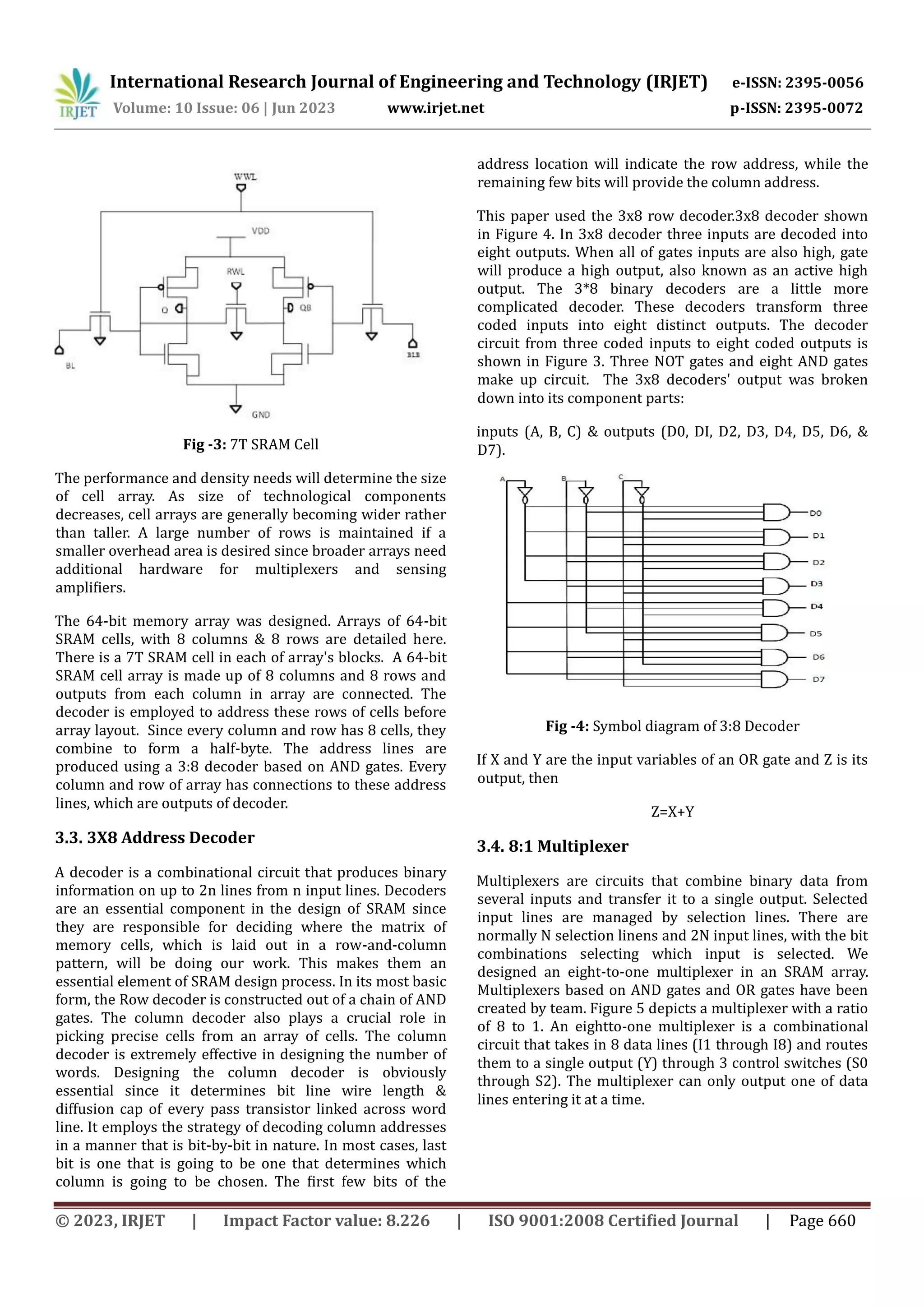
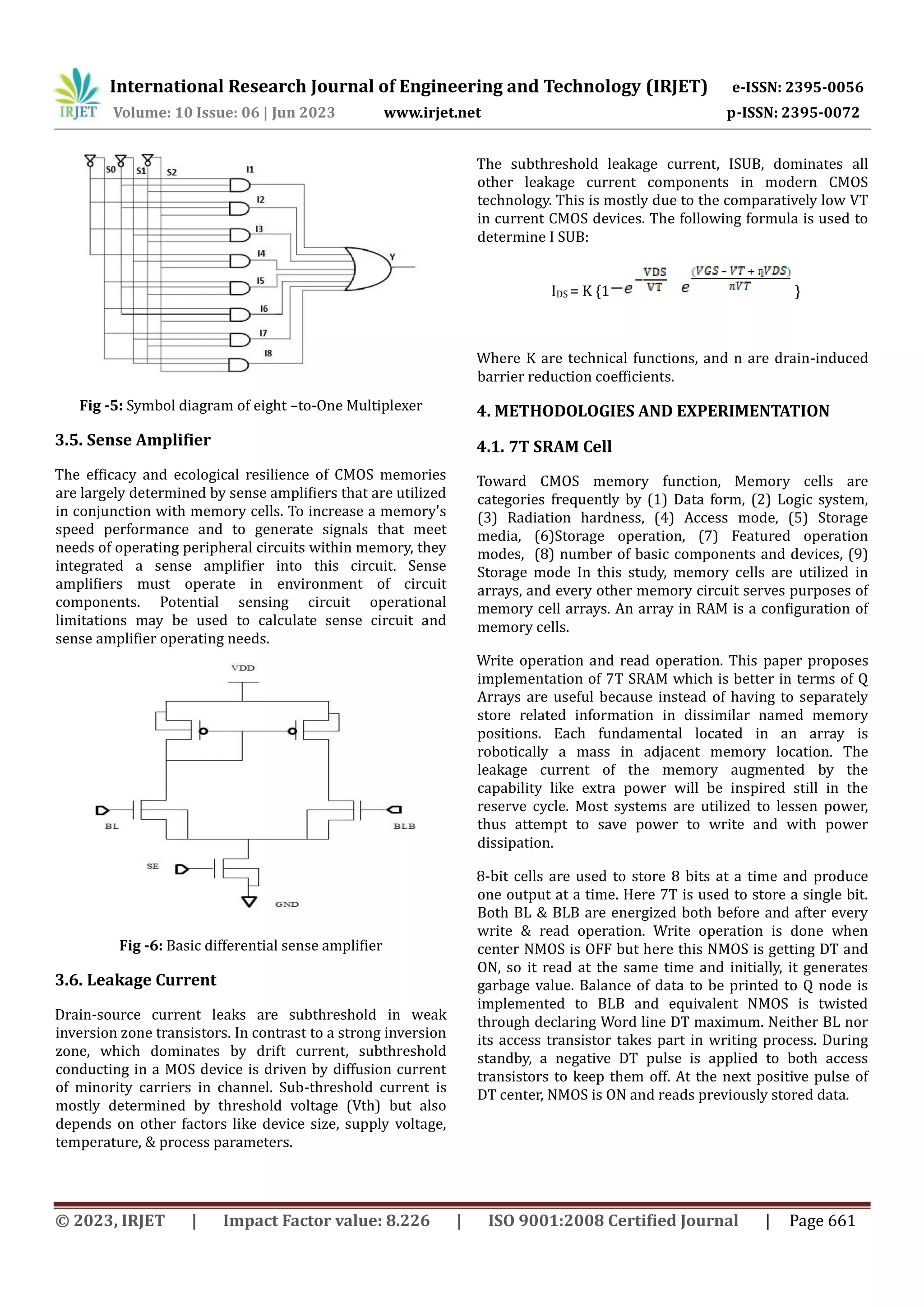
![© 2023, IRJET | Impact Factor value: 8.226 | ISO 9001:2008 Certified Journal | Page 659 technology library. To increase performance and reduce power consumption while resolving issues with regular SRAM cells. Shyam Akashe et al. [27] produced a 5-transistor read static noise margin-free SRAM cell. They created this one- of-a-kind cell by using memory value stream of ordinary software, which has a significant bias towards zero at bit level. The primary research discovery that informed this design was that cell leakage is quantified at node where transistor is disabled. Assuming similar design assumptions, the suggested cell area was 21.66 percent smaller than 6T SRAM cell and increased speed by 28.57 percent. The suggested cell's endurance, which mimics 45 nm technology, was calculated using suitable write-read operations. Additionally, the latency of revolutionary cell was reduced by 70 percent when compared to that of a conventional SRAM cell with 6 transistors. The recommended cell's memory cell access leakage current was 72.10 percent lower than that of a 6T SRAM cell, even though leakage current tripled every 10 degrees Celsius. 3. SRAM MEMORY ARRAY ARCHITECTURE SRAM memory array-producing organization is shown in Figure 1. Word-oriented or bit-oriented SRAM arrays may be built. A single bit of data may be accessed from any point in a bit-oriented structure. In contrast, SRAM's word- oriented design translates every address to a word with n data bits. A word-oriented column decoder or column mux may partition a single sense amplifier across 2,4, or more columns using "K" address bits. A single sense amplifier reads many columns in bit-oriented organization architecture, ensuring accuracy. The SRAM array included sensing amplifiers, write driver circuits, column decoders, row decoders, a 1-bit 7T SRAM cell, & precharge circuits In memory array arrangements, the precharge circuit was used to equalize bit lines prior to operating mode. SRAM memory array implementation is shown in Figure 2. [28][29][30][31][32]. Fig -1: Architecture of SRAM array. Fig -2: Realization of SRAM array Multiplexers, address decoders, Cell arrays, and sense amplifiers make up a standard SRAM block. The operation and layout of every element are briefly covered in sections that follow. 3.1. SRAM Cell As long as power is supplied to circuit, a static RAM cell can keep a data bit securely stored in memory. There are two access transistors that allow for reading and writing and a central storage cell that consists of 2 cross-coupled inverters linked to a Subthreshold NMOS transistor that prevents data loss. A word line carrying a control signal determines whether or not an access transistor is conducting. When word line is high, both access transistors conduct and allow for writing and reading of data bits. It insulates the storage cell when word line is low. The input & output nodes of storage cell are connected to data lines that are balanced with one another by an access transistor. Before a read operation starts, the bit lines in computer memory are commonly pre-charged to a reference voltage which is very near to positive supply voltage. 3.2. Read/Write Operation Each read and write operation begins and ends with a large charge on BLB & BL. To begin the process of writing to 7T cell, MN7 is disabled. By asserting WWL high, we switch on MN1 and disable MN2, preparing node Q to receive data with its complement. Both BL and MN2 are ignored throughout the writing process. While WL and WR are asserted low by MN1 or MN2 in standby mode, W is asserted high by MN7. A 7T cell's read operation is equivalent to a 6T cell. During read process, BLB discharges down the critical read path, which includes MN1, MN7, and MN6, with QB storing "0." The "1" stored in QB is discharged by BL along read routes MN2 & MN3 during read operation. International Research Journal of Engineering and Technology (IRJET) e-ISSN: 2395-0056 Volume: 10 Issue: 06 | Jun 2023 www.irjet.net p-ISSN: 2395-0072](https://image.slidesharecdn.com/irjet-v10i6101-230711092443-3bb09c7a/75/Design-and-Performance-Evaluation-of-a-64-bit-SRAM-Memory-Array-Utilizing-Modern-Deep-Submicron-Technology-3-2048.jpg)
![International Research Journal of Engineering and Technology (IRJET) e-ISSN: 2395-0056 Volume: 10 Issue: 06 | Jun 2023 www.irjet.net p-ISSN: 2395-0072 © 2023, IRJET | Impact Factor value: 8.226 | ISO 9001:2008 Certified Journal | Page 664 Table3 Comparison with Previous Result Performance Parameter Previous work [33] Proposed work Total Low Power 30.90nW 27.6nW 7. CONCLUSIONS A novel 64-bit SRAM memory array design architecture is presented in this research. Memory consumes two types of power: primary and secondary. Due to this work intend a 7T-based SRAM cell, which addresses the vital causes intended for a low-power SRAM in profound modern submicron expertise along with recommended techniques utilized to conquer them. According to this work the presented SRAM construction is examined and next a fundamental 7T SRAM construction was selected. This 64- bit SRAM memory array has been implemented both ways and investigated separately. While designing the 64-bit SRAM memory using 7T-based SRAM cell to minimize the Leakage Power, working Low Power, and improve the Read and Write access time. CMOS Based 7T SRAM using Adaptive body bias technique is suitable for implementation which is characterized by high speed with minimum leakage current, and low power compared with 7T SRAM. To avoid performance changes with low power, we investigate the usage of adaptive body biassing to be utilized to manage the substrate voltages of transistors. The future design of a 64bit SRAM memory array is similar to that of a 64-bit SRAM memory array, which uses a regular 6T SRAM cell and a single additional NMOS transistor positioned between two cross-linked inverters. This design reduces reserve mode static power. Cadence simulation tool is used in 90nm contemporary deep submicron technologies. REFERENCES [1] S. Mishra, A. Dubey, S. S. Tomar, and S. Akashe, “Design and Simulation of High Level Low Power 7T SRAM Cell Using Various Process & Circuit Techniques,” 2012. [2] S. Akashe, M. Shastri, and S. Sharma, “Multi Vt 7T SRAM cell for high speed application at 45 nm technology,” 2012. doi: 10.1063/1.4751560. [3] B. N. K. Reddy, K. Sarangam, T. Veeraiah, and R. Cheruku, “SRAM cell with better read and write stability with Minimum area,” 2019. doi: 10.1109/TENCON.2019.8929593. [4] B. Alorda, G. Torrens, S. Bota, and J. Segura, “8T vs. 6T SRAM cell radiation robustness: A comparative analysis,” 2011. doi: 10.1016/j.microrel.2010.09.002. [5] B. N. K. Reddy, C. Ramalingaswamy, R. Nagulapalli, and D. Ramesh, “A novel 8T SRAM with improved cell density,” Analog Integr. Circuits Signal Process., 2019, doi: 10.1007/s10470-018-1309-z. [6] S. Gnanavel et al., “Analysis of Fault Classifiers to Detect the Faults and Node Failures in a Wireless Sensor Network,” Electron., 2022, doi: 10.3390/electronics11101609. [7] K. Radhakrishnan, D. Ramakrishnan, O. I. Khalaf, M. Uddin, C. L. Chen, and C. M. Wu, “A Novel Deep Learning-Based Cooperative Communication Channel Model for Wireless Underground Sensor Networks,” Sensors, 2022, doi: 10.3390/s22124475. [8] Y. Liu et al., “Interaction-Enhanced and Time-Aware Graph Convolutional Network for Successive Point- ofInterest Recommendation in Traveling Enterprises,” IEEE Trans. Ind. Informatics, 2023, doi: 10.1109/TII.2022.3200067. [9] O. I. Khalaf et al., “Blinder Oaxaca and Wilk Neutrosophic Fuzzy Set-based IoT Sensor Communication for Remote Healthcare Analysis,” IEEE Access, 2022, doi: 10.1109/ACCESS.2022.3207751. [10] A. F. Subahi, O. I. Khalaf, Y. Alotaibi, R. Natarajan, N. Mahadev, and T. Ramesh, “Modified Self-Adaptive Bayesian Algorithm for Smart Heart Disease Prediction in IoT System,” Sustain., 2022, doi: 10.3390/su142114208. [11] U. M. Janniekode, R. P. Somineni, O. I. Khalaf, M. M. Itani, J. Chinna Babu, and G. M. Abdulsahib, “A Symmetric Novel 8T3R Non-Volatile SRAM Cell for Embedded Applications,” Symmetry (Basel)., 2022, doi: 10.3390/sym14040768. [12] D. Saha and S. K. Sarkar, “High-speed reduced-leakage SRAM memory cell design techniques for low-power 65 nm FD-SOI/SON CMOS technology,” Microelectronics J., 2014, doi: 10.1016/j.mejo.2014.04.032. [13] P. S. Bellerimath and R. M. Banakar, “Implementation of 16X16 SRAM Memory Array using 180nm Technology,” no. Ncwse, pp. 288–292, 2013. [14] A. S. Kumar and T. V. K. H. Rao, “Scalable benchmark synthesis for performance evaluation of NoC core mapping,” Microprocess. Microsyst., 2020, doi: 10.1016/j.micpro.2020.103272. [15] A. S. Kumar and T. V. K. H. Rao, “An adaptive core mapping algorithm on NoC for future heterogeneous system-on-chip,” Comput. Electr. Eng., vol. 95, no.](https://image.slidesharecdn.com/irjet-v10i6101-230711092443-3bb09c7a/75/Design-and-Performance-Evaluation-of-a-64-bit-SRAM-Memory-Array-Utilizing-Modern-Deep-Submicron-Technology-8-2048.jpg)
![International Research Journal of Engineering and Technology (IRJET) e-ISSN: 2395-0056 Volume: 10 Issue: 06 | Jun 2023 www.irjet.net p-ISSN: 2395-0072 © 2023, IRJET | Impact Factor value: 8.226 | ISO 9001:2008 Certified Journal | Page 665 September, p. 107441, 2021, doi: 10.1016/j.compeleceng.2021.107441. [16] T. V. K. Hanumantha Rao and A. S. A. I. Kumar, “Performance assessment of adaptive core mapping for NoC-based architectures,” Int. J. Embed. Syst., 2022, doi: 10.1504/ijes.2022.10050537. [17] A. Sai Kumar and T. V. K. Hanumantha Rao, “An Efficient Low Latency Router Architecture for MeshBased NoC,” 2021. doi: 10.1007/978-981-33- 40589_21. [18] A. S. Kumar, T. V. K. H. Rao, and B. N. K. Reddy, “Performance and communication energy constrained embedded benchmark for fault tolerant core mapping onto NoC architectures,” Int. J. Ad Hoc Ubiquitous Comput., 2022, doi: 10.1504/IJAHUC.2022.125427. [19] A. S. Kumar and B. Naresh Kumar Reddy, “An Efficient Real-Time Embedded Application Mapping for NoC Based Multiprocessor System on Chip,” Wirel. Pers. Commun., 2023, doi: 10.1007/s11277-022-10080-x. [20] A. S. Kumar and T. V. K. H. Rao, “Efficient core mapping on customization of NoC platforms,” 2019. doi: 10.1109/iSES47678.2019.00025. [21] B. Kaleeswari and S. Kaja Mohideen, “Design, Implementation and Analysis of 8T SRAM Cell in Memory Array,” Int. J. Eng. Technol., 2018, doi: 10.14419/ijet.v7i3.1.16808. [22] J. Shrivas, “Impact of Design Parameter on SRAM Bit Cell,” pp. 355–358, 2012, doi: 10.1109/ACCT.2012.63. [23] S. Singh and S. Akashe, “Low Power Consuming 1 KB (32 × 32) Memory Array Using Compact 7T SRAM Cell,” Wirel. Pers. Commun., 2017, doi: 10.1007/s11277-0174226-z. [24] C. A. Gong, C. Hong, K. Yao, and M. Shiue, “A Low- Power Area-Efficient SRAM with Enhanced Read Stability in 0 . 18- µ m CMOS,” pp. 729–732, 2008. [25] R. Bisht, P. Aggarwal, P. Karki, and P. Pande, “Low power and noise resistant 16×16 SRAM array design using CMOS logic and differential sense amplifier,” 2017. doi: 10.1109/CCAA.2016.7813954. [26] H. Banga, “Implementation of 16x16 SRAM Memory Array,” 2017 Int. Conf. Recent Innov. Signal Process. Embed. Syst., pp. 458–462, 2017, doi: 10.1109/RISE.2017.8378199. [27] S. Akashe, S. Bhushan, and S. Sharma, “High density and low leakage current based 5T SRAM cell using 45 nm technology,” 2011. doi: 10.1109/ICONSET.2011.6167978. [28] B. V. Garidepalli, R. Prasad Somineni, A. Peddi, and U. M. Janniekode, “Design and Analysis of 16nm GNRFET and CMOS Based Low Power 4kb SRAM Array Using 1-Bit 6T SRAM Cell,” 2022. doi: 10.1109/GlobConET53749.2022.9872358. [29] S. Singhal, N. Jatana, A. F. Subahi, C. Gupta, O. I. Khalaf, and Y. Alotaibi, “Fault Coverage-Based Test Case Prioritization and Selection Using African Buffalo Optimization,” Comput. Mater. Contin., 2023, doi: 10.32604/cmc.2023.032308. [30] H. Rahman, J. Tariq, M. A. Masood, A. F. Subahi, O. I. Khalaf, and Y. Alotaibi, “Multi-Tier Sentiment Analysis of Social Media Text Using Supervised Machine Learning,” Comput. Mater. Contin., 2023, doi: 10.32604/cmc.2023.033190. [31] B. N. K. Reddy, A. James, and A. S. Kumar, “FaultTolerant Core Mapping for NoC based architectures with improved Performance and Energy Efficiency,” 2022. doi: 10.1109/ICECS202256217.2022.9970825. [32] A. Sai Kumar, U. Siddhesh, N. Sai Kiran, and K. Bhavitha, “Design of High Speed 8-bit Vedic Multiplier using Brent Kung Adders,” 2022. doi: 10.1109/ICCCNT54827.2022.9984591. [33] M. K. Kumari, D. Upadhyay, and S. Jahan, “Optimization Of Low Power Digital Vlsi Using High Speed Sram,” vol. 18, no. 6, pp. 326–333, 2021.](https://image.slidesharecdn.com/irjet-v10i6101-230711092443-3bb09c7a/75/Design-and-Performance-Evaluation-of-a-64-bit-SRAM-Memory-Array-Utilizing-Modern-Deep-Submicron-Technology-9-2048.jpg)

This document summarizes a research paper that designed and evaluated the performance of a 64-bit SRAM memory array using modern deep submicron technology. The key points are: 1) A 64-bit SRAM memory array was designed using a 1-bit 7T SRAM cell and implemented in a 8x8 bit configuration using CMOS technology and a 0.7 volt supply. 2) The 7T SRAM cell design aimed to reduce leakage power during read/write operations and improve noise immunity at low voltages. 3) Simulation results showed the 64-bit SRAM array had lower read and write power consumption compared to 8T and 7T SRAM designs.