The document presents a novel automated PCB identification and defect-detection system (APIDS) utilizing machine vision techniques to enhance the efficiency of quality assurance processes in the PCB manufacturing industry. It focuses on reducing human intervention by implementing a method that identifies the type of PCB before defect inspection, achieving identification accuracies of 98.66% and 100% for database and camera images, respectively. The system demonstrates a high defect detection accuracy of 92.3% under controlled conditions, leveraging feature extraction techniques such as SURF and ORB for image processing.
![International Journal of Electrical and Computer Engineering (IJECE) Vol. 9, No. 1, February 2019, pp. 297~306 ISSN: 2088-8708, DOI: 10.11591/ijece.v9i1.pp297-306 297 Journal homepage: http://iaescore.com/journals/index.php/IJECE Automated PCB identification and defect-detection system (APIDS) Shams Ur Rehman, Ka Fei Thang, Nai Shyan Lai School of Engineering, Faculty of Computing, Engineering & Technology, Asia Pacific University of Technology & Innovation, Malaysia Article Info ABSTRACT Article history: Received Apr 12, 2018 Revised Jun 25, 2018 Accepted Sep 10, 2018 Ever growing PCB industry requires automation during manufacturing process to produce defect free products. Machine Vision is widely used as popular means of inspection to find defects in PCBs. However, it is still largely dependent on user input to select algorithm set for the PCB under inspection prior to the beginning of the process. Continuous increase in computation power of computers and image quality of image acquisition devices demands new methods for further automation. This paper proposes a new method to achieve further automation by identifying the type of PCB under inspection prior to begin defect inspection process. Identification of PCB is achieved by using local feature detectors SURF and ORB and using the orientation data acquired to transform the PCB image to the reference image for inspection of defects. A close-loop system is produced as a prototype to reflect the practicality of the idea. A Graphical User Interface was developed using MATLAB to present the proposed system. Test data contained 29 PCBs. Each PCB was tested 5 times for camera acquired images and 3 times for database images. The identification accuracy is 98.66% for database images and 100% for images acquired from the camera. The time taken to detect the model of PCB is recorded and is significantly lower for ORB based identification than SURF based. The system is also a close loop system which detects defects in PCB units. The detection of defects has highest accuracy of 92.3% for best controlled environment scenario. With controlled environment, the system could detect defects in PCB pertaining to smallest of components such as SMDs. Keywords: Machine vision ORB PCB defects PCB identification SURF Copyright © 2019 Institute of Advanced Engineering and Science. All rights reserved. Corresponding Author: Ka Fei Thang, School of Engineering, Faculty of Computing, Engineering & Technology, Asia Pacific University of Technology & Innovation, Malaysia. Email: dr.ka.fei@apu.edu.my 1. INTRODUCTION The PCB industry is ever-growing and according to [1], the need is for reliable and accurate vision system because PCBs manufactured today has much more component density than earlier and it continues to grow. Study by [2] shows that PCB industry is expected to reach US$ 93.9 billion in 2017. Manufacturers want their products defect free to satisfy their customer needs and remain up par with the competitors. Once a product is manufactured in a plant, it has to go through a quality assurance process to ensure that the product that is being sold to the customer does not have any defects. In this process the product under inspection is tested for defects and flaws. Most manufacturers prefer means of non-destructive inspection system such as Computer Vision for their products quality assurance. Computer Vision also known as Machine Vision in industrial applications is the process of extracting digital information from an image of a scene and then utilizing that information to achieve](https://image.slidesharecdn.com/3312657-200714080037/75/Automated-PCB-identification-and-defect-detection-system-APIDS-1-2048.jpg)
![ ISSN: 2088-8708 Int J Elec & Comp Eng, Vol. 9, No. 1, February 2019 : 297 - 306 298 different tasks [3]. Computer vision has vast applications in the quality assurance field. A survey conducted in [4] describes the importance of computer vision in quality assurance in different industries such as component manufacturing, integrated circuits, printing, glass manufacturing etc. To utilize computer vision effectively in quality assurance system, it should have the following steps [4]: a. Image Acquisition b. Image Processing c. Feature Extraction d. Decision Making Existing inspection systems to detect defects in the PCBs are not fully automated and require human input in differentiating the type and model of the PCB under inspection to scan for defects. When manufactured products are undergone through a computer vision assisted quality assurance process, the algorithm set is manually selected and controlled by the operator of the machine. While the accuracy of the existing systems is acceptable, it still relies on human input for algorithm selection. Incorporating PCB identification prior to inspection in quality assurance is required to reduce human input and fully automate the inspection process. This paper suggests a method to train an Automated Optical Inspection (AOI) bot to recognize the PCBs from the existing database of the manufacturer. This would allow the bot to inspect different products under a single inspection cycle without manually setting up pre-programmed algorithm for each product (Manual identification). The proposed method could allow a manufacturer successfully implement or improve their Just in Time (JIT) manufacturing [5] and allow for fully automated inspection process with minimal requirement of human input in the process. 1.1. Related Work There is plenty of research work focused on pattern recognition in PCB industry. The idea of using local features for pattern recognition and describing the algorithm as Scale Invarient Feature Transform (SIFT) due to the robustness of the algorithm to changes in scale of the images or different affine transformations was proposed by Lowe [6]. Szymanski & Stemmer [2] proposed classification of the defects of PCB boards in small series production using SIFT features. Recent advancement in pattern recognition is the algorithm called FAsT-Match which works on minimizing the Sum of Absolute Differences (SAD) error [7]. Operations such as scaling, translation, rotation etc. can interfere with the recognition result of other algorithms due to explosion. This developed algorithm deals with the issue by discretizing the space of affine transformations. This work achieved accurate detection result on different images of varying sizes and experimental result on RealWorld scenarios. SIFT pattern matching involves calculation of log of Gaussian which is time consuming. Speeded-Up Robust Features (SURF) is an upgraded version of SIFT [8]. SURF differs from SIFT in regard as it takes approximation of log of Gaussian using Box Filter which speeds up the recognition process. Related pattern recognition study in differentiate and matching different types of leaves from a database to find the type of the plant was proposed and comparative study was performed on Histogram of Oriented Gradients (HOG), Local Binary Pattern (LBP) and SURF [9]. SURF is termed as optimal interest point detector when detecting objects based on interest points [10]. Current advent of AI provides human-like ability of decision making to machines. Combined with vision capability, machine learning approaches for pattern recognition bears great results. Studies utilizing machine learning techniques using Neural Networks (NN) [11], [12] are in favor of classifying objects using patterns in images on a large scale. Recent research based on similar area on classification of PCB for recycling and retirement purposes [13] also undertake similar methodologies as proposed in this paper. However, that work does not utilize further data obtained from classification to proceed with defect detection in PCB units. Defect detection techniques in machine vision culminate to be the crux of PCB inspection in any inspection equipment. Throughout the years, various research works has been undertaken to advance the algorithms in this field. Information obtained from RGB color spectrum can be utilized to find the flux defect in IC pins [14]. Most techniques involves comparing image under inspection to a reference image to find the variation and describe the irregularities as faults in the PCB [15]. Background subtraction techniques used by Sundaraj [16] in the color spectrum to find missing components or misaligned components using Mixture of Gaussian method has procured high accuracy. Machine learning techniques have helped to to detect and classify different types of solder joints based on reduction method with the help of neural networks and genetic algorithm trained to classify the defects based on the irradiated color from the solder joints [17]. 2. PROPOSED SYSTEM To minimize the human input that is provided to inspection machines prior to inspection process, the machine must be aware of the type of the circuit board that is under inspection so that it can load relevant](https://image.slidesharecdn.com/3312657-200714080037/75/Automated-PCB-identification-and-defect-detection-system-APIDS-2-2048.jpg)
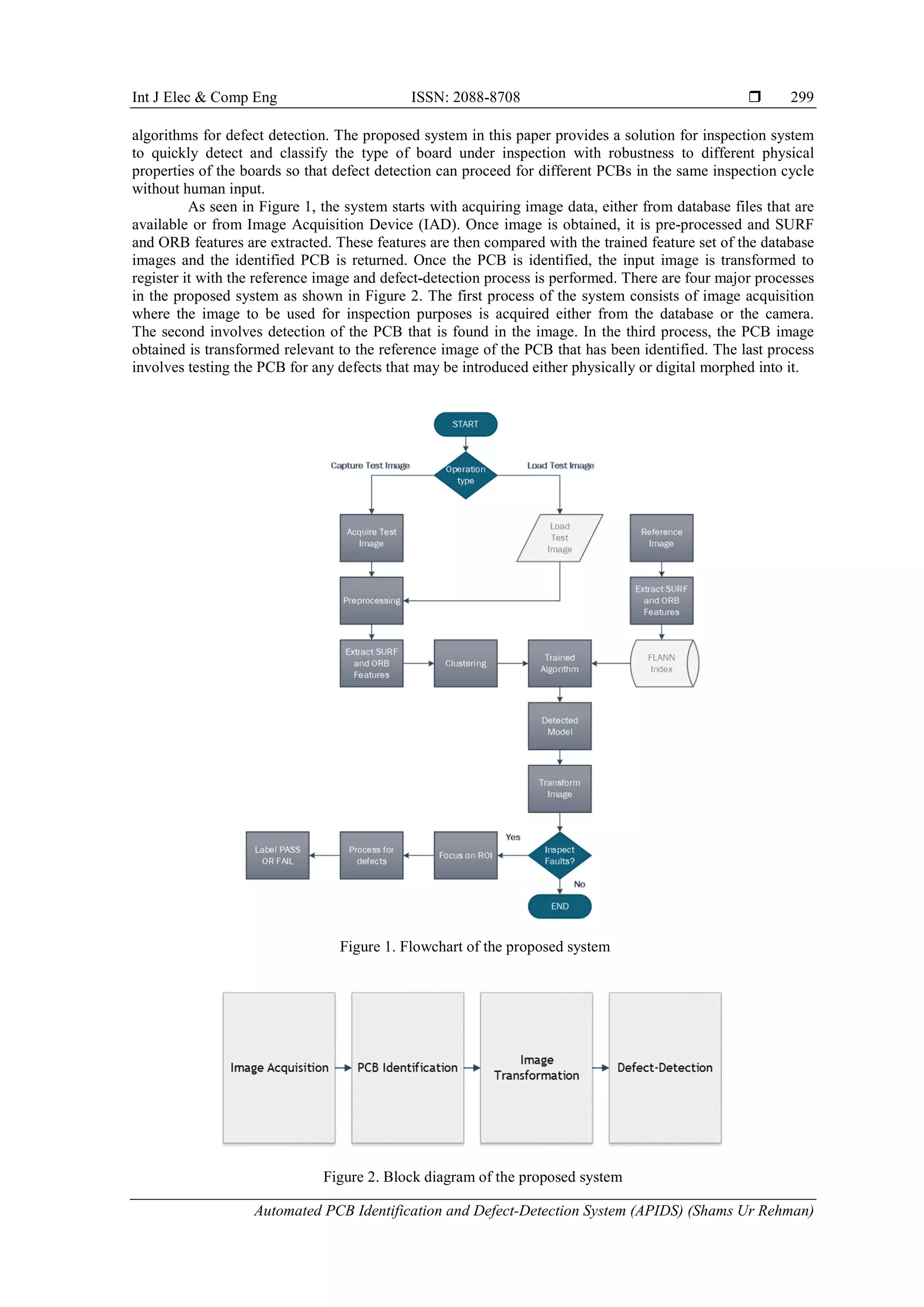
![ ISSN: 2088-8708 Int J Elec & Comp Eng, Vol. 9, No. 1, February 2019 : 297 - 306 300 2.1. Image acquisition The images were obtained with a smartphone camera having specification of 12MP Dual Pixel sensor, f/1.7 aperture, LED flash, OIS (Optical Image Stabilisation) with a resolution of 4032x3024. Image dataset was obtained from the work submitted for free research use in previous study [13]. During the operation of the camera, a focused image was sent wirelessly from the camera to MATLAB for processing. Higher resolution was selected to provide meaningful data for image processing as the electronic density on the PCB is high. 2.2. PCB identification Once the image is obtained, SURF and ORB keypoints are detected. Keypoint is an image location in spatial coordinate where physical features in the image may lie such as corner points. For SURF keypoints, each of keypoint detected is assigned an orientation obtained from wavelet responses in the x and y direction for neighborhood of 6s, where s is the scale. A neighborhood region is divided into 4x4 sub regions and the wavelet response for both x and y direction gives the vector used to transform the images [8]. For ORB keypoints, centroid based on weighted intensity is found inside a small patch of pixels where the feature (corner point) is maintained at the center of the patch. The direction vector between the corner point and the centroid provides the orientation data [18]. Once the keypoints are detected, a descriptor is used to describe the keypoints detected. A descriptor is an algorithm that summarizes the neighborhood around the keypoint to describe a feature by differentiating it from other features thus providing pattern recognition ability. These SURF or ORB points are then compared with a database of other similar points stored in a database. The database basically includes long list of these SURF points or ORB points for all the images to be compared with. To cluster the SURF points of the newly acquired image to the database, Fast Approximate Nearest Neighbor Search Library (FLANN) index is used. It provides nearest search algorithm and works well for large databases. This is helpful to keep the detection time to its minimum even if the database contains large number of feature points for SURF. ORB points are matched using a BruteForce technique by finding the Hamming distance of the points which compares a point of interest in one image to all the points in other images stored in the database. Once the points are clustered, the matches in each PCB are tabulated and highest performer is picked as the detected PCB. For SURF-based identification, the FLANN index is trained before every PCB identification. 2.3. Image transformation Once the keypoints are matched, outliers are excluded using the M-estimator SAmple Consensus (MSAC) algorithm. The process of registration of the input image to the reference image is similar to [19] where R-RANSAC algorithm is used instead to find the outliers. Out of the inliers, 2 points are selected to transform the image acquired to the reference image in the database. This gives a transformation matrix that can be used to warp the image of the PCB under inspection to the reference image of the matched PCB in the database. This registers the input image to the reference image where defect-detection can be performed. 2.4. Defect detection The transformed image is then compared with reference image to find the defects in the PCB. The types of defects to detect in this paper are kept missing components and scratches on the PCB as defect detection is the secondary objective. The algorithm for fault detections takes a dont-care part of the image which is not in the ROI defined by the user for selected reference image. This is done to minimize the effect of poorly achieved controlled environment for the prototype built due to budget limitation. The ROIs declared by the user is used to obtain two masks for filtering the image with to obtain dont-care pixels in the image. The ROIs are stored in a structure with information about the potential defect that the ROI is for. These are specified before the inspection process. In industrial application, defect detection algorithms are tailored to customer needs. The transformed image obtained in the previous step is in RGB color model. Each of the channels is extracted from the image. The absolute difference of each of the channel in the transformed image and reference image is found for each pixel of input image denoted by I and reference image by R where x and y are the spatial coordinates and c is the color channel R, G, and B given in (1). This highlights changes in the input image based on the reference image. Color information is used to obtain better detection of missing components where PCB board itself is identical in color to the component to a certain level where subtraction of Gray level image might result in loss of information. Absolute difference equation shown in (1). AbsoluteDifference = |Ic(x, y) − Rc(x, y)| (1)](https://image.slidesharecdn.com/3312657-200714080037/75/Automated-PCB-identification-and-defect-detection-system-APIDS-4-2048.jpg)
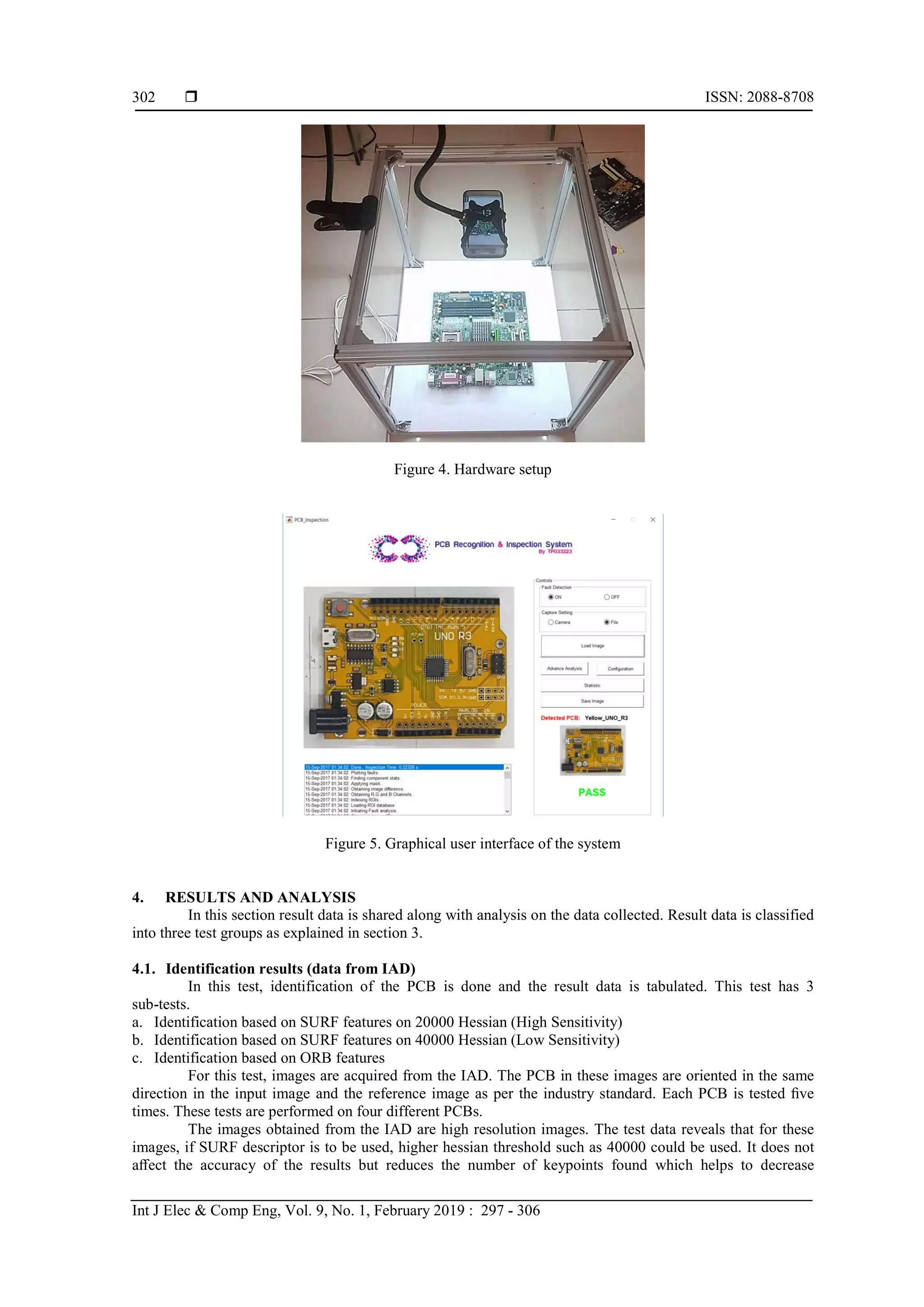
![Int J Elec & Comp Eng ISSN: 2088-8708 Automated PCB Identification and Defect-Detection System (APIDS) (Shams Ur Rehman) 301 The resultant images are thresholded to an 8bit value ranging between (0-255) of the image intensity to obtain logical binary images. This value is amendable by the user. This is done to remove the noise produced by the image registration, as there will always be a certain noise after the absolute difference of the images. The masks obtained prior are then filtered with the logical image to consider the area outside the ROIs as dont-care region. Additional noise is removed using median filter of 5x5 neighborhoods and followed by morphological operations to identify changes in the components as blobs. If the area size of the blob is greater than a threshold value for both missing component and scratches, the blob is classified as a defect. The defect detection process is depicted in Figure 3. Figure 3. Defect detection process illustration 3. EXPERIMENTAL SETUP MATLAB was used for programming the system. Image Processing toolbox libraries were utilized along with OpenCV libraries [20] available as a wrapper for MATLAB in form of mexOpenCV. This wrapper was used to reduce identification time significantly as compared to matching SURF and ORB points using MATLAB libraries because of the large size of the images in this case. A prototype was constructed to act as an image acquisition station. The bed for placing the PCB was 44x40 cm in dimension. LEDs strips were used to provide a control environment to a certain degree. The hardware implementation of the prototype is presented in Figure 4. The hardware was not able to achieve completely uniform controlled lightening environment to mimic industrial equipment. A GUI was designed carefully considering the user friendly approaches to challenges. Configuration button is especially included to perform soft changes such as training for new boards to the code using setting file which is stored locally in a file for future use. The main window of the GUI is presented in Figure 5. There are total of 6 tests, grouped into 3, performed on the system to evaluate the accuracy of the result, overall efficiency and speed of the system. These tests are listed as follows: a. Classification (data from IAD) b. Classification (database files) c. Defect-detection Classification tests are performed on the images acquired using IAD or the database files. Both set of images have different resolutions than one another. The test images obtained from a database set are in different orientation too. These differences in the quality of images result in different behavior of the applied algorithms. These tests are focused on the timing of the tasks and matching of features between these images and the accuracy of classification. The third test is fault detection test based on different faults introduced to the PCB images acquired from IAD. These faults, as mentioned in section 3 may be introduced digitally or physically to the PCB.](https://image.slidesharecdn.com/3312657-200714080037/75/Automated-PCB-identification-and-defect-detection-system-APIDS-5-2048.jpg)
![Int J Elec & Comp Eng ISSN: 2088-8708 Automated PCB Identification and Defect-Detection System (APIDS) (Shams Ur Rehman) 303 computational time. This is the sensitivity of the SURF features. From Table 1 it can be deduced that detection time is based on the number of keypoints that are found and matches from those keypoints which is in turn dependent on the sensitivity of the SURF. So SURF based identification could be speed up if the sensitivity is lowered. The ORB extractor extracts constant 500 keypoints from the image. Match ratio represents that ratio of matches to the keypoints. It can be observed that SURF with lower sensitivity, the average matching ratio is the highest which proves it to be more reliable for images where the image quality corresponds to the quality of images available for this test i.e. high resolution images. Majority of the time consumed during the process is taken by the setup time in which matching of features process initializes. From the Table 1, it can be observed that while ORB based detection is fastest, it results in weaker match ratio. The identification accuracy of using the SURF and ORB features for this set of images is 100%. Table 1. Averages of the Data Obtained from IAD Conducted on 20 Images Feature extractor Setup time (s) Detection time (s) Transformation time (s) Total time (s) Matches Keypoints Match ratio SURF (20k) 0.649 1.043 0.115 1.807 476.55 744.7 0.665 SURF (40k) 0.481 0.934 0.119 1.534 131.75 156.6 0.795 ORB 0.659 0.321 0.121 1.101 287.9 500 0.576 4.2. Identication results (database images) The database is trained to compute SURF features of 54 images where SURF hessian threshold to obtain SURF features is set to 20,000. Lower hessian threshold has to be used than the one used for the IAD files as they are higher resolution than this. Four of these images, obtained from the IAD are also included in this database. 25 PCBs are selected for testing where each PCB has three images. Each image is of resolution 2464x1640. 2 out of 3 images for each PCB have difference in the orientation to the one used as reference in the trained database. Each PCB image is presented for identification 3 times and changes in orientation has also occurred. Table 2 shows the averages of the result data obtained. From the table, it can be observed that identification based on ORB is a lot faster than SURF complying with the test done on IAD images in Table 1. During the testing, drop in matching ratio was experience over the course of the experiment. This drop in the matching ratio is explained by the change in orientation. This does not hinder the identification process. Total images test are 75 (3 for each PCB, 25 total PCB). 74 were identified correctly in both cases. The identification accuracy for the system based on image data also containing oriented images for both SURF and ORB based feature is 98.66%. Table 2. Averages of the Data Obtained from Database from 75 Images Feature extractor Setup time (s) Detection time (s) Transformation time (s) Total time (s) Matches Keypoints Match ratio SURF 0.713 0.385 0.060 1.158 90.64 111 0.777 ORB 0.700 0.147 0.055 0.902 306.72 500 0.613 The detection rate for both database images and IAD images is comparatively superior to other methods of classification using SURF features [9] based on leaves and Feedforward Neural Network (FNN) classification based on fruits [21]. In terms of similar classification performed on PCBs, the detection accuracy is similar to [13], the time consumption is far more compared to the same study. 4.3. Defect detection result This test is a measurement of accuracy of the fault detection algorithm employed to detect either missing components or scratches on PCB. The dont-care region is neglected based on the ROI which the user registers it for each PCB in the configuration menu. This ROI selection ensures that minor noises which are caused by changes in the illumination or view point are avoided as in industrial grade equipment, the noise could be minimized by conducting the process under controlled environment. Two types of defects are tried to be identified by the algorithm; missing component (MC) and Scratched Components (SC). The MC and SC are identified and drawn over the input image to be displayed to the user. The images that are selected for testing the accuracy of fault detection algorithm and tabulating the results are obtained from IAD. The images are then saved locally and digitally modified to have defects in the PCB. All defects are introduced to single image of the PCB, however, this image is not the same as the reference image. The image resolution is 4032x3024. The test samples include 4 PCBs with numerous defects.](https://image.slidesharecdn.com/3312657-200714080037/75/Automated-PCB-identification-and-defect-detection-system-APIDS-7-2048.jpg)
![ ISSN: 2088-8708 Int J Elec & Comp Eng, Vol. 9, No. 1, February 2019 : 297 - 306 304 Table 3 shows the accuracy of the identified faults. The highest accuracy of 100% is achieved while testing the Arduino UNO R3. Fault in the Arduino board was made by removing a chip from its location then the algorithm was tested on it. However, the chip removed was fairly large in size. The program sends cropped image of the missing component to the output folder which is shown in Figure 6. Asrock 960GC GS board has almost perfect alignment with reference image. Hence, in this case, the surrounding environment is fairly controlled. Further data is collected on performing same test with different threshold values and it is tabulated in Table 4. The increasing accuracy of the result when threshold decreases signifies that with control environment provided, the algorithm can work to achieve higher efficiency and accurate results. The accuracy score for lowest threshold in the experiment shows that the algorithm performs similar to other methods of defect detection [16]. Low threshold values cannot be used for images where there is error in image registration process and this error can be depicted as defect. For the tested PCB, when the threshold values were decreased, it also detected faults in smaller components such as SMDs. Figure 6. Missing components output data Table 3. Defect Detection Data (Threshold MC 70, SC 50) PCB defects detected false score MC SC MC SC +ve Acer Board 4 6 4 4 0 80 Asrock 960GC GS 5 8 4 5 0 69.2 Yellow UNO R3 6 5 5 1 0 54.5 Arduino UNO R3 1 0 1 0 0 100 Table 4. Defect-detection Result of 'Asrock 960GC GS' at Various Threshold Threshold defects detected false score (MC/SC) 0-255 MC SC MC SC +ve 70/50 5 8 4 5 0 69.2 60/40 5 8 4 6 0 76.9 50/30 5 8 5 7 0 92.3 35/25 5 8 5 7 0 92.3 4.4. Possible sources of errors There are number of factors that can negatively influence the result of the applied algorithm. While the identification is seamlessly executed, the defect-detection process is subjected to certain errors. During observation, the transformation matrix obtained to warp the input image gives better result when SURF features are used. ORB features produces bit of noise when the images are compared. Due to this error, lower threshold values for MC and SC detection underperforms and produces false positives. Due to uncontrolled lightening environment, detection of darker components on a darker shaded PCB is also limited and prone to errors.](https://image.slidesharecdn.com/3312657-200714080037/75/Automated-PCB-identification-and-defect-detection-system-APIDS-8-2048.jpg)
![Int J Elec & Comp Eng ISSN: 2088-8708 Automated PCB Identification and Defect-Detection System (APIDS) (Shams Ur Rehman) 305 5. CONCLUSION AND FUTURE WORK The aim of the project is develop a system that would allow different products for processing with pattern recognition and image processing that would help provide the manufacturer with different product testing under single inspection cycle. The ideology behind the project was allow PCB inspection equipment with machine vision to identify the PCB model and make decision based on the result of the identification, in this case, PCB defect-detection. PCB identification in this system prior to inspection process has been achieved using feature detectors and descriptors which is a pattern recognition method. The identification rate gives of 98.66% for 75 database images and 100% for 20 IAD images. The defect detection algorithm developed accuracy of 92.3% for best case scenario performs very well in comparison with other methods for similar problem. The accuracy of defect-detection is subjected to many factors but with controlled environment provided, it can be significantly improved for all types of PCBs. The complete system is implemented with having a user friendly GUI to operate the system with. Multiple tests are performed on the test to evaluate different parameters of the system. The test results obtained focuses on the speed and accuracy of the algorithms. Proposed system was developed to simplify the Machine Vision based QC process. However, the system that has been implemented is not perfect and have limitation. While the speed of the system is a fraction of a second and considered fast, Machine Vision inspection system is relatively faster. Therefore, the speed of the system needs to be further improved. Some methods could be made simpler with next version of the program. Defect-detection process needs improvement as it is only based on detection of missing components in the PCB or scratches on any components and is not consider to be very reliable during our testing. However, this process could be largely improved by accessing controller environment of the obtained images. If the histogram of the image is in higher region for all channels, it also induces the incapability of the program to distinguish between a bad component and a false positive. The system developed could be improved upon further research or recommendation based modification. The program is written in MATLAB which is a high level language, the speed of the system could easily be improved by translating it into a low level language such as C++ where OpenCV library is more easily available to use. The image registration process method could also be replaced with a better performing method to avoid errors in next process due noise after image registration. However, this could also be achieved by providing controlled environment. To conclude, machine vision inspection equipment can perform better if equipped with identification techniques to base the decisions on. Moreover, a machine vision friendly color standards could set for PCB manufacturers to color the components and PCB in certain standards for easier recognition of the components or the defects in the PCBs. REFERENCES [1] T. Chen, J. Zhang, and Y. Zhou, “A Smart Machine Vision System for PCB Inspection,” Eng. Intell. Syst., pp. 513– 518, 2001. [2] C. Szymanski and M. R. Stemmer, “Automated PCB Inspection in Small Series Production based on SIFT Algorithm,” IEEE Int. Symp. Ind. Electron., vol. 2015–Septe, pp. 594–599, 2015. [3] A. Rosenfeld, “Computer vision: Basic principles.,” Proc. IEEE, vol. 76, no. 8, pp. 863–868, 1988. [4] E. N. Malamas, E. G. M. Petrakis, M. Zervakis, L. Petit, and J. D. Legat, “A Survey on Industrial Vision Systems, Applications and Tools,” Image Vis. Comput., vol. 21, no. 2, pp. 171–188, 2003. [5] C. A. Swanson and W. M. Lankford, “Just-in-time Manufacturing,” Bus. Process Manag. J., vol. 4, no. 4, pp. 333– 341, 1998. [6] D. G. Lowe, “Distinctive Image Features From Scale-Invariant Keypoints,” Int. J. Comput. Vis., 2004. [7] S. Korman, D. Reichman, G. Tsur, and S. Avidan, “Fast-Match: Fast Affine Template Matching,” Int. J. Comput. Vis., pp. 1–15, 2016. [8] H. Bay, A. Ess, T. Tuytelaars, and L. Van Gool, “Speeded-Up Robust Features (SURF),” Comput. Vis. Image Underst., 2008. [9] Z. Ibrahim, N. Sabri, and N. N. Abu Mangshor, “Leaf Recognition using Texture Features for Herbal Plant Identification,” vol. 9, no. 1, pp. 152–156, 2018. [10] A. M. Ahsan and D. Bin Mohamad, “Features Extraction for Object Detection Based on Interest Point,” vol. 11, no. 5, pp. 2716–2722, 2013. [11] J. Stallkamp, M. Schlipsing, J. Salmen, and C. Igel, “Man vs. computer: Benchmarking machine learning algorithms for traffic sign recognition,” Neural Networks, vol. 32, pp. 323–332, Aug. 2012. [12] A. Krizhevsky, I. Sutskever, and G. E. Hinton, “ImageNet Classification with Deep Convolutional Neural Networks,” Adv. Neural Inf. Process. Syst., pp. 1–9, 2012. [13] C. Pramerdorfer and M. Kampel, “PCB Recognition using Local Features for Recycling Purposes,” Proc. 10th Int. Conf. Comput. Vis. Theory Appl., no. January, pp. 71–78, 2015. [14] TeohOng, “Computer Machine Vision Inspection on Printed Circuit Boards Flux Defects,” Am. J. Eng. Appl. Sci., vol. 6, no. 3, pp. 263–273, 2013.](https://image.slidesharecdn.com/3312657-200714080037/75/Automated-PCB-identification-and-defect-detection-system-APIDS-9-2048.jpg)
![ ISSN: 2088-8708 Int J Elec & Comp Eng, Vol. 9, No. 1, February 2019 : 297 - 306 306 [15] S. Singh and M. Bharti, “Image Processing Based Automatic Visual Inspection System for PCBs,” IOSR J. Eng., vol. 2, no. 6, pp. 1451–1455, 2012. [16] K. Sundaraj, “PCB Inspection for Missing or Misaligned Components Using Background Subtraction,” WSEAS Trans. Inf. Sci. Appl., vol. 6, no. 5, pp. 778–787, 2009. [17] H. Wu, X. Zhang, Y. Kuang, G. Ouyang, and H. Xie, “Solder Joint Inspection based on Neural Network Combined with Genetic Algorithm,” Optik (Stuttg)., vol. 124, no. 20, pp. 4110–4116, 2013. [18] E. Rublee, V. Rabaud, K. Konolige, and G. Bradski, “ORB: An Efficient Alternative to SIFT or SURF,” Proc. IEEE Int. Conf. Comput. Vis., pp. 2564–2571, 2011. [19] Z. Gu, L. Cai, Y. Yin, Y. Ding, and H. Kan, “Registration of Brain Medical Images Based on SURF Algorithm and R-RANSAC Algorithm,” vol. 12, no. 3, pp. 2290–2297, 2014. [20] G. Bradski, “The OpenCV Library,” Dr. Dobb’s J. Softw. Tools, 2000. [21] Y. Zhang, S. Wang, G. Ji, and P. Phillips, “Fruit Classification Using Computer Vision and Feedforward Neural Network,” J. Food Eng., vol. 143, pp. 167–177, 2014. BIOGRAPHIES OF AUTHORS Shams Ur Rehman received his BEng. (Hons) degree in Mechatronic Engineering from Asia Pacific University, Kuala Lumpur and keen on specializing in image processing and computer vision field. A conscientious and responsible individual, who has keen interest in science and its applications. Ka Fei, Thang graduated with a Doctor of Philosophy in Electrical Engineering and a Bachelor of Engineering (Honours) degree in Electrical and Electronic Engineering from the University of Bath, UK. He is also a Chartered Engineer and a member of the Institution of Engineering and Technology (IET), UK. Dr Thang is now serving Asia Pacific University of Technology and Innovation (APU) as Associate Professor and Head of School of Engineering. His responsibilities are to manage the quality processes of the School in teaching and learning as well as ensuring continuous professional accreditation for all the engineering programmes. N. S. Lai born in Seremban, Malaysia, is currently an Associate Professor at School of Engineering, Asia Pacific University of Technology & Innovation, working in the area of micro- and nano-electronics. He received his B. Eng. (Hons) in Electrical Engineering (2007) and Ph.D. in the field of Silicon-Based Nano-electronics and Radiation Detectors (2012) from University of New South Wales, Australia. His main research interest includes semiconductor micro- and nano-fabrication, quantum dot devices, low temperature (milli-Kelvin) measurements, and semiconductor microdosimeters.](https://image.slidesharecdn.com/3312657-200714080037/75/Automated-PCB-identification-and-defect-detection-system-APIDS-10-2048.jpg)