This paper presents a method for detecting and classifying faults in printed circuit boards (PCBs) using image processing techniques, specifically image subtraction algorithms. It addresses challenges such as image orientation and size variations, ultimately aiming to improve quality assurance while reducing labor costs in PCB manufacturing. The proposed approach successfully identifies commonly occurring faults like missing conductors and etching defects, and offers a more efficient preprocessing and classification method compared to previous works.
![International Journal on Recent and Innovation Trends in Computing and Communication ISSN: 2321-8169 Volume: 5 Issue: 7 206 – 210 _______________________________________________________________________________________________ 206 IJRITCC | July 2017, Available @ http://www.ijritcc.org _______________________________________________________________________________________ An Image Based PCB Fault Detection And Its Classification Sridhar B K Master of Technology in Industrial Electronics, Department of ECE, Sri Jayachamarajendra College of Engineering Mysuru, India sridharbk15@gmail.com V Nattarasu Associate Professor, Department of ECE, Sri Jayachamarajendra College of Engineering Mysuru,India nattarasu@gmail.com Abstract- The field of electronics is skyrocketing like never before. The habitat for the electronic components is a printed circuit board (PCB). With the advent of newer and finer technologies it has almost become impossible to detect the faults in a printed circuit board manually which consumes lot of manpower and time. This paper proposes a simple and cost effective method of fault diagnosis in a PCB using image processing techniques. In addition to fault detection and its classification this paper addresses various problems faced during the pre-processing phase. This paper overcomes the drawbacks of the previous works such as improper orientations of the image and size variations of the image. Basically image subtraction algorithm is used for fault detection. The most commonly occurring faults are concentrated in this work and the same are implemented using MATLAB tool. Keywords-PCB, fault, orientation,size correction, image subtraction __________________________________________________*****_________________________________________________ I. INTRODUCTION Industrial automation is one of the booming fields today. Automation helps in reducing a lot of manpower and time. The same applies to printed circuit board (PCB) manufacturing industries. One of the highest costs in manufacturing PCBs is visual inspection which includes various manual methods. So there is a tradeoff between cost and quality. The quality assurance is always important in an industry thus it is required to achieve maximum quality of a product with minimal cost. Printed circuit defects are those defects which brings a deviation from the normal characteristics and functionality of a PCB. Any missing element or any extra elements on the board which is not intended is referred to as a defect. PCB defects can be categorized into two types namely functional defects and structural defects. Functional defects are those defects which are pertaining to the functionality of the circuit or the overall system. These are troublesome in nature. The other kind of the defect is called structural defect. It is also often referred to as cosmetic defects. Cosmetic defects refer to the changes in the appearance of the circuit board. The PCB manufacturing process is based on chemical and mechanical actions that may damage the intended design. Computer generated printed circuit board are those images which are defect free. These are often known as Base images/Template Images. These are designed as control images to compare with the image that contains defects. This paper proposes a method which overcomes the drawbacks of the existing works such as improper orientations of the image and size variations of the image. Basically image subtraction algorithm is used for fault detection. With few modifications to image subtraction algorithm the faults can be classified into separate types. The majorly occurring faults in a PCB are missing conductors, etching, wrong size hole, missing hole and pinhole. Along with these some problems with the image orientation and size variation corrections which takes place during preprocessing phase are addressed in this work. II. LITERATURE SURVEY [1] This paper has discussed about detection of faults using image subtraction technique and the classification of the defects into various groups. They discuss the various possible ways of fault detection in a PCB alongside defects are categories into seven groups with a minimum of one defect and up to a maximum of 4 defects in each group using MATLAB image processing tools this research separates two of the existing groups containing two defects each into four new groups containing one defect each by processing synthetic images of bare through-hole single layer PCBs. [2] This paper has proposed a method for defect detection and classification for the faults in a PCB. Image subtraction algorithm has been used for finding the defects and separate algorithms with further modifications have been implemented. In this work a base image is read and stored. An inspection image is compared with the stored image and is subtracted to give out the results. The main algorithm remains the same i.e, image subtraction. The other subsidiary algorithms are used for classifying the faults individually rather than in groups. [3] This paper deals with the fault detection of assembled PCBs where the inspection is done even after assembling the components with the PCB. [4] This paper enhances the work by inspecting the solder pasted PCBs. [5] This work brings up](https://image.slidesharecdn.com/41150027406617-07-2017-171227114549/75/An-Image-Based-PCB-Fault-Detection-and-Its-Classification-1-2048.jpg)
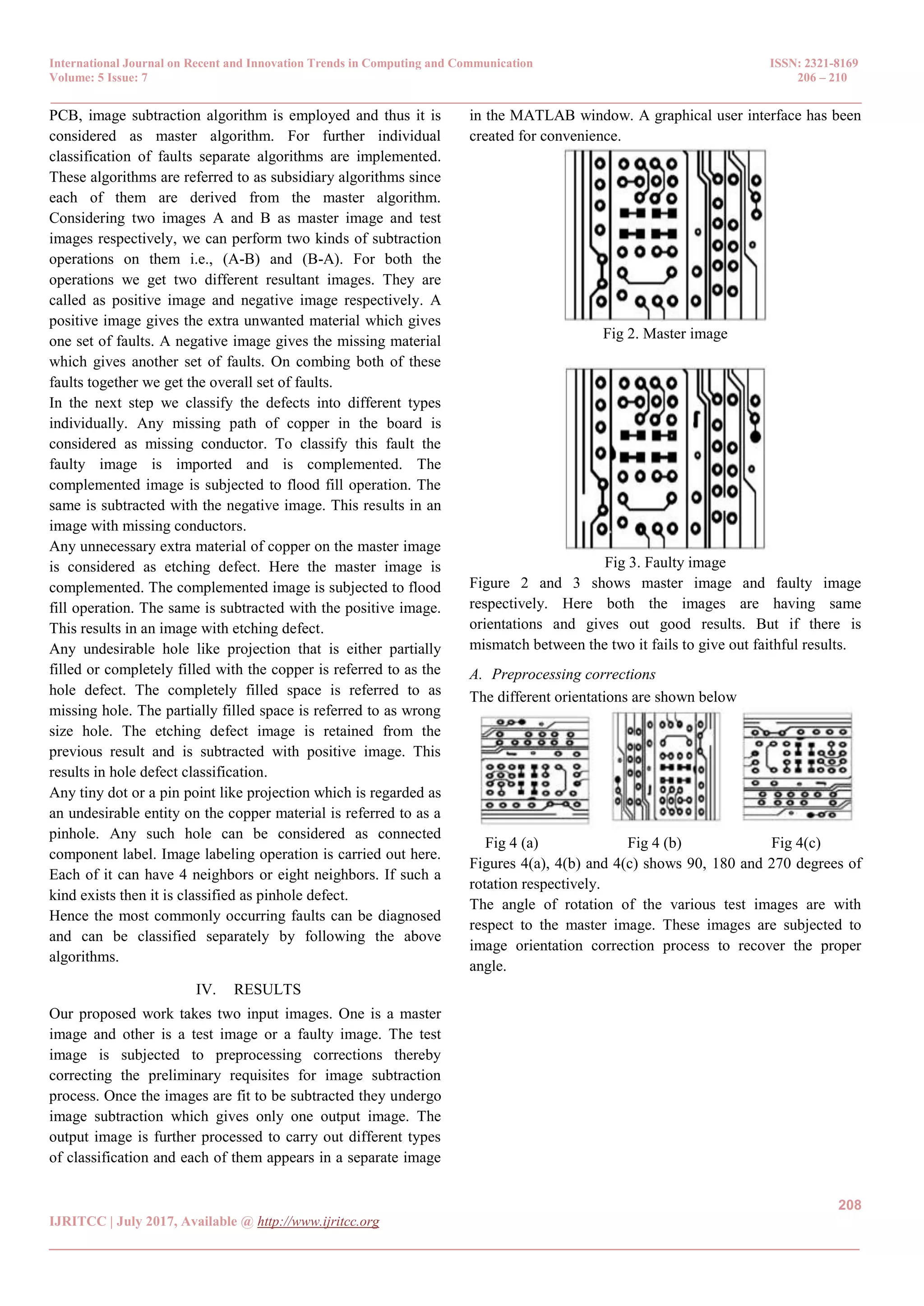
![International Journal on Recent and Innovation Trends in Computing and Communication ISSN: 2321-8169 Volume: 5 Issue: 7 206 – 210 _______________________________________________________________________________________________ 207 IJRITCC | July 2017, Available @ http://www.ijritcc.org _______________________________________________________________________________________ the concept of neural networks in order to address the situation of solder joints inspection combined with sophisticated genetic algorithm. [6] This paper presents the techniques used to inspect the defects on Surface Mount PCBs. The technique of windowing is employed to reduce the amount of redundant data to be processed and computation time. Even though there are plenty of algorithms to find the faults in a PCB using image processing techniques, there are only few methods to classify those defects and group them. Individual defects cannot be found out accurately. Thus they are formed in groups. Thus one can improve the method by increasing the classification of the faults and enhance the existing group numbers to a higher number of groups so that one can easily find which fault has occurred in particular. Also some pre processing techniques such as image orientation and size correction can be implemented. III. METHODOLOGY A. Problem Statement The current techniques give focus on defect detection and defect classification. But our method proposes a system which addresses few problems such as irregular orientations and irregular sizes of test images when compared with the master image. Thus the problem is to correct these preliminary requisites. B. Problem Formulation Various pre processing techniques like orientation correction and size correction are done in the first phase. The later phase includes defect detection and followed by defect classification. Thus it is a three tier procedure. Figure 1. Pre processing Techniques. C. System Implementation The test image is first read in MATLAB environment. For image orientation correction first we check various angles such as 90, 180 and 270 degrees. Thus there are 3 test cases for image orientation correction. Once we are done with image orientation correction we proceed further for image size correction. Although it is not a sequential procedure the figure1 just shows the flow. Thus image size correction is done to the test image if any. The previous methods have few drawbacks one of them being the image orientation. Image orientation is regarded as very important thing because if the orientation of the images are not matched with each other it fails to give out the correct results. The image can be tilted in any direction. As a test case 3 important orientations are addressed in our work. They are namely 90, 180 and 270 degrees. The algorithm proposes recursive steps of tilt angle correction. Once it is matched with the original image, faults can be found out and can be classified individually. The other drawback of the existing work is that the arbitrary sizes of the images which doesn’t give proper results. If the sizes aren’t properly matched it is impossible to carry out image subtraction. When the size of the master image doesn’t match with that of test image this problem occurs. If the image is of improper size or not cropped properly the pixel values doesn’t match each other. In such case size correction is necessarily required for computation failing to which we will not be able to proceed further. D. Proposed Algorithm The proposed methodology for image orientation correction is carried out by following steps Import a master image Read the column values of the master image Import a test image Read the column values of the test image Compare both the values If the compared values are same then subtract the images else correct the orientation by some angle of tilt recursively until both of them match with each other The proposed methodology for image size correction is carried out by following steps Import a master image Read the row values of the master image Import a test image Read the row values of the test image Compare both the values If the compared values are same then subtract the images else correct the size by comparing each pixel value with the master image pixel value similar to windowing technique. Having done with the preprocessing techniques we enter the mainstream of PCB faults detection. A PCB can have as many as 14 different types of faults. 1.Missing conductor 2.Pin hole 3.Wrong size hole 4.Etching Defect 5.Missing hole 6.Breakout 7.Spur 8.Short 9.Open circuit 10.Conductors too close 11.Spurious copper 12.Excessive short 13.Mouse bite 14.Overetch. Out of these some of the most commonly occurring faults are numbered from 1 to 5 namely Missing conductor, Pin hole, Wrong size hole, Etching Defect and Missing hole. So this work mainly concentrates on diagnosing these faults and classifying them individually rather than in groups. Once the pre processing steps are taken care the next step is to find the defects in the PCB. To find the overall defects in the](https://image.slidesharecdn.com/41150027406617-07-2017-171227114549/75/An-Image-Based-PCB-Fault-Detection-and-Its-Classification-2-2048.jpg)
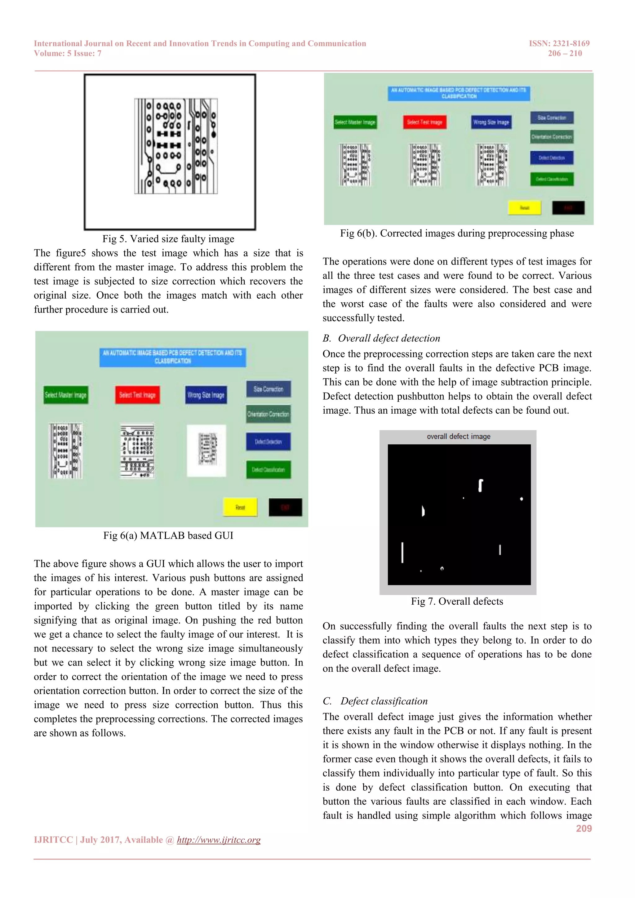
![International Journal on Recent and Innovation Trends in Computing and Communication ISSN: 2321-8169 Volume: 5 Issue: 7 206 – 210 _______________________________________________________________________________________________ 210 IJRITCC | July 2017, Available @ http://www.ijritcc.org _______________________________________________________________________________________ subtraction algorithm followed by image complementation, image flood fill operation and image indexing operations as common procedures with slight difference to each of it. By implementing each algorithm faults can be classified and distinguished clearly without any ambiguity. Fig 8(a) Missing conductor Fig 8(b) Etching defect Fig 8(c) Hole defects Fig 8(d) Pinhole defect V. CONCLUSION AND FUTURE SCOPE Our work overcomes the existing drawbacks such as improper orientations of test image with respect to master image and improper sizes of test image compared to master image. In addition to that our work successfully detects the defects in a PCB image and classifies the same accurately. This method provides less time complexity when compared with other segmentation procedures. As a future scope one can develop an IC which can test the PCB and classify the defects in one single go. REFERENCES [1] Siti Hazurah Indera Putera, Syahrul Fahmi Dzafaruddin, Maziah Mohamad Shah Alam, “MATLAB based defect detection and classification of printed circuit board” IEEE transaction 2012. [2] Beant Kaur, Gurmeet Kaur, Amandeep Kaur, “Detection and classification of printed circuit board defects using image subtraction method”, IEEE transaction 2014 [3] D.-M. Tsai,C.-H.Yang, "A Quantile-Quantile Plot Based Pattern Matching for Defect Detection", Pattern Recognition Letters, Vo1.26, pp.1948-1962, 2005 [4] IF.Borba and J. Facun, "A Printed Circuit Board Automated Inspection System", 38th IEEE Midwest Symposium on Circuits and System, Vol. I, pp.69-72, 1996. [5] J.Jiang, J.Cheng and D.Tao, "Color Biological Features-Based Solder Paste Defects Detection and Classification on Printed Circuit Boards", IEEE Transactions on Components, Packaging and Manufacturing Technology, Vol.2, No.9, pp.IS36-IS44, 2012. [6] C.Benedek, "Detection of Soldering Defects in Printed Circuit Boards with Hierarchical Marked Point Processes", Pattern Recognition Letters, Vo1.32, pp.IS3S-IS43,2011 . [7] Chu Xianghu, ZengXiangjun, Deng Feng, Li Ling, “Novel PCB Sensor based on Rogowski Coil for Transmission Lines Fault Detection”2009 IEEE [8] Shih-Yuan Huang, Chi-Wu Mao, and Kuo-Sheng ChengA VQ- Based Approach to Thermal Image Analysis for Printed Circuit Boards DiagnosisIEEE Transactions on Instrumentation and Measurement, Vol. 54, No. 6, December 2005. [9] Chu Xianghu, ZengXiangjun, Deng Feng, Li Ling, “Novel PCB Sensor based on Rogowski Coil for Transmission Lines Fault Detection”2009 IEEE. [10] Wan Jiuqing, Li Xingshan “PCB Infrared Thermal Imaging Diagnosis using Support Vector Classifier”Proceedings of the 4th World Congress on Intelligent Control and Automation June 10- 14, 2002, Shanghai, P.R.China.](https://image.slidesharecdn.com/41150027406617-07-2017-171227114549/75/An-Image-Based-PCB-Fault-Detection-and-Its-Classification-5-2048.jpg)