
![Bit-band Operation Example For example, in order to set bit[3] in word data in address0x20000000 ;Read-Modify-Write Operation ;Bit-band Operation LDR R1, =0x20000000 ;Setup address LDR R1, =0x2200000C ;Setup address LDR R0, [R1] ;Read MOV R0, #1 ;Load data ORR.W R0, #0x8 ;Modify bit STR R0, [R1] ;Write STR R0, [R1]](https://image.slidesharecdn.com/arm-m4-programmer-model-160808184351/75/Arm-cortex-m4-programmer-model-10-2048.jpg)
![• Read-Modify-Write operation – Read the real data address (0x20000000) – Modify the desired bit (retain other bits unchanged) – Write the modified data back • Bit-band operation – Directly set the bit by writing ‘1’ to address 0x2200000C,which is the alias address of the fourth bit of the 32-bit data at 0x20000000 – In effect, this single instruction is mapped to 2 bus trans-fers: read data from 0x20000000 to the buffer, and then write to 0x20000000 from the buffer with bit [3] set](https://image.slidesharecdn.com/arm-m4-programmer-model-160808184351/75/Arm-cortex-m4-programmer-model-11-2048.jpg)
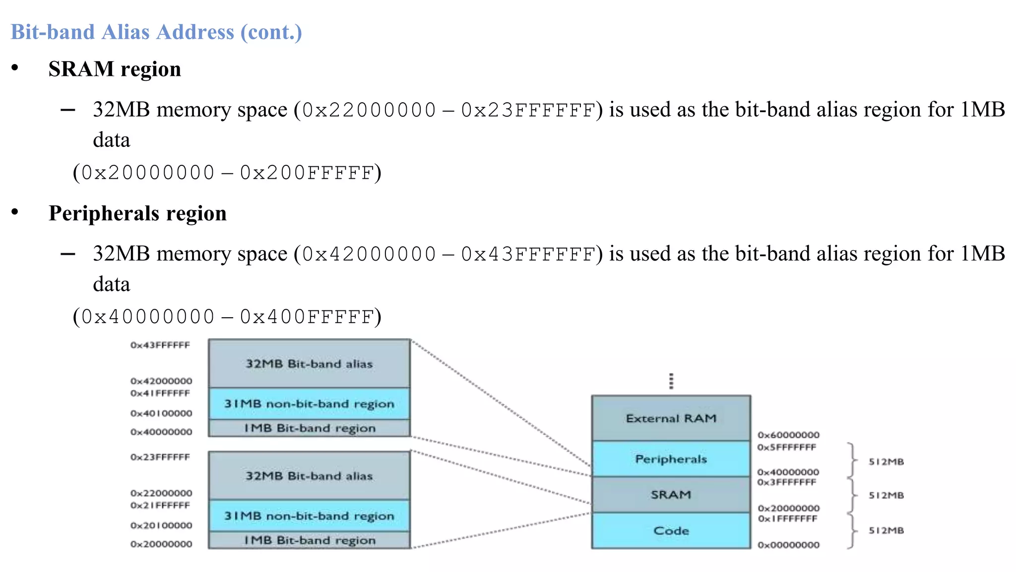
![Bit-band Alias Address Each bit of the 32-bit data is one-to-one mapped to the bit-band alias address – For example, the fourth bit (bit [3]) of the data at0x20000000 is mapped to the bit-band alias address at 0x2200000C – Hence, to set bit [3] of the data at 0x20000000, we only need to write ‘1’ to address 0x2200000C – In Cortex-M4, there are two pre-defined bit-band alias regions: one for SRAM region, and one for peripherals region](https://image.slidesharecdn.com/arm-m4-programmer-model-160808184351/75/Arm-cortex-m4-programmer-model-12-2048.jpg)
![Benefits of Bit-Band Operations • Faster bit operations • Fewer instructions • Atomic operation, avoid hazards – For example, if an interrupt is triggered and served during the Read-Modify-Write operations, and the interrupt service routine modifies the same data, a data conflict will occur Interrupt occurs Read data at 0x00 Modify bit [1] Read data at0x00 Modify bit [1] Write data back Write data back Interrupt returns Bit [1] modifiedby ISR is overwritten by the main program Main program](https://image.slidesharecdn.com/arm-m4-programmer-model-160808184351/75/Arm-cortex-m4-programmer-model-14-2048.jpg)
![Byte3 Byte2 Byte1 Byte0 Word 3 Byte3 Byte2 Byte1 Byte0 Word 2 Byte3 Byte2 Byte1 Byte0 Little [31:24] Word 1 endian 32-bit memory [23:16] [15:8] [7:0] Byte0 Byte1 Byte2 Byte3 Word 3 Byte0 Byte1 Byte2 Byte3 Word 2 Byte0 Byte1 Byte2 Byte3 Address [31:24] [23:16] [15:8] [7:0]](https://image.slidesharecdn.com/arm-m4-programmer-model-160808184351/75/Arm-cortex-m4-programmer-model-18-2048.jpg)


The document outlines the ARM Cortex-M4F programming model, detailing the memory map, instructions, and bit-band operations. It explains the structure of the memory regions used for code, SRAM, peripherals, and external devices, as well as the benefits of utilizing bit-band operations for efficient single-bit manipulation. Additionally, it covers the ARM and Thumb instruction sets, highlighting the Cortex-M4's support for 32-bit Thumb-2 instructions, which optimize performance without the need for state switching.
Introduction to the ARM programming series focusing on Cortex-M4, presented by Mohammed Gomaa.
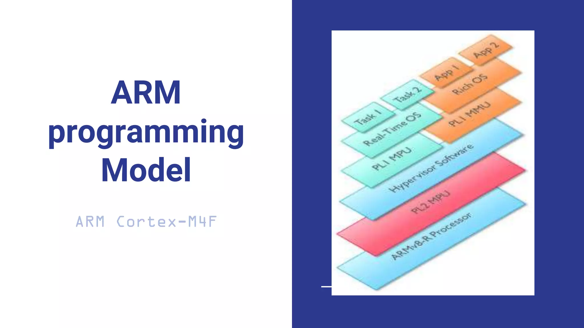
Introduction to ARM programming model using the ARM Cortex-M4F processor.
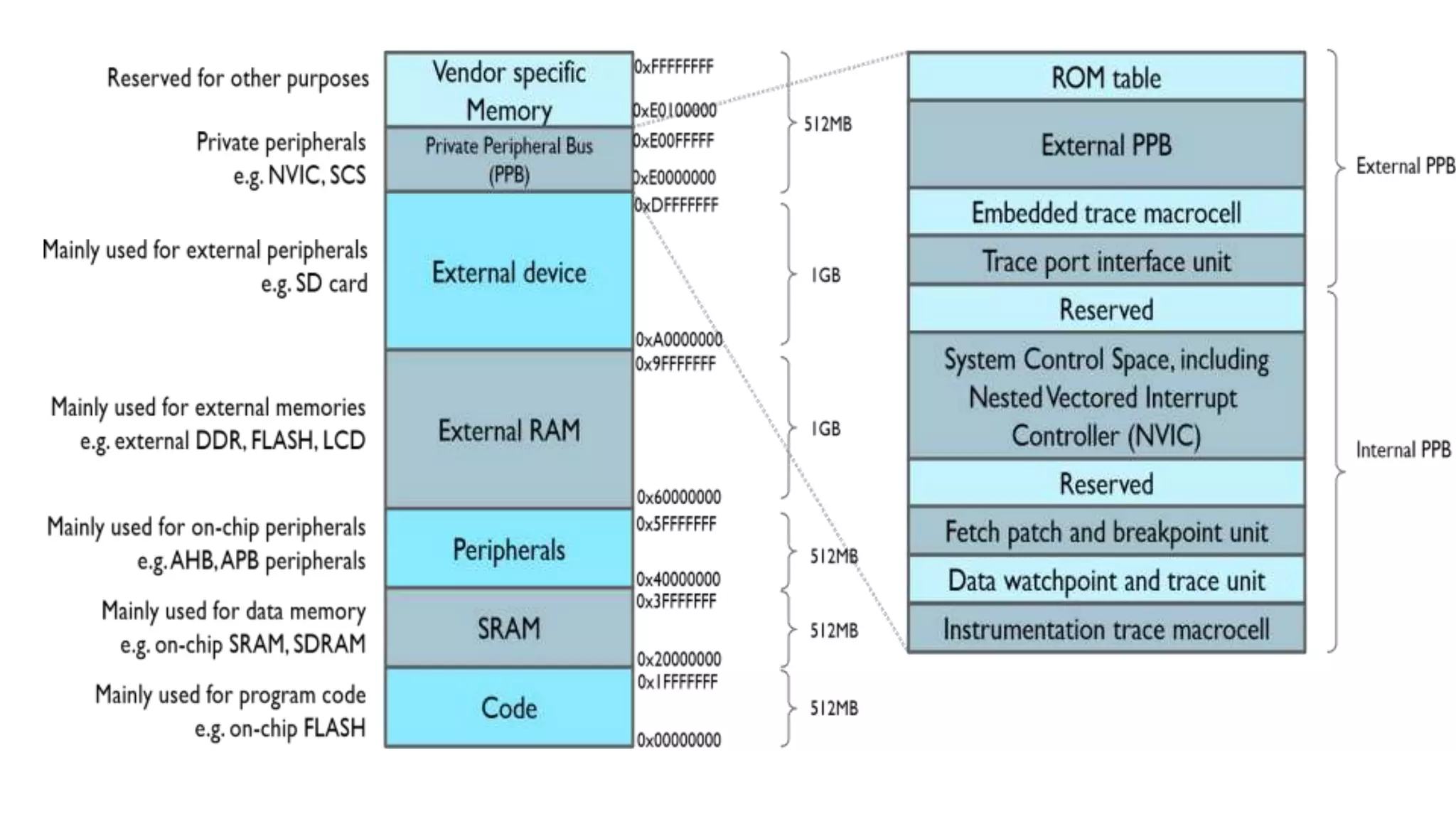
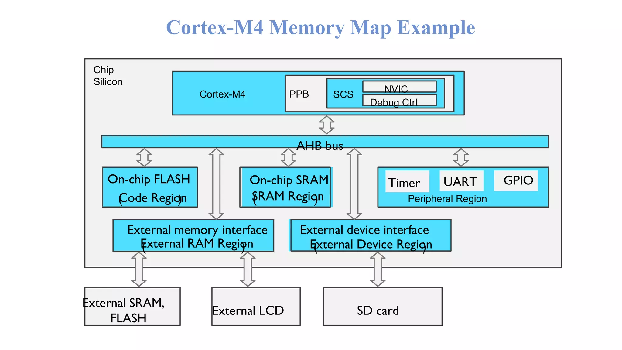
Overview of Cortex-M4 Memory Map, including memory address space and the ARM Cortex-M4 instruction set.
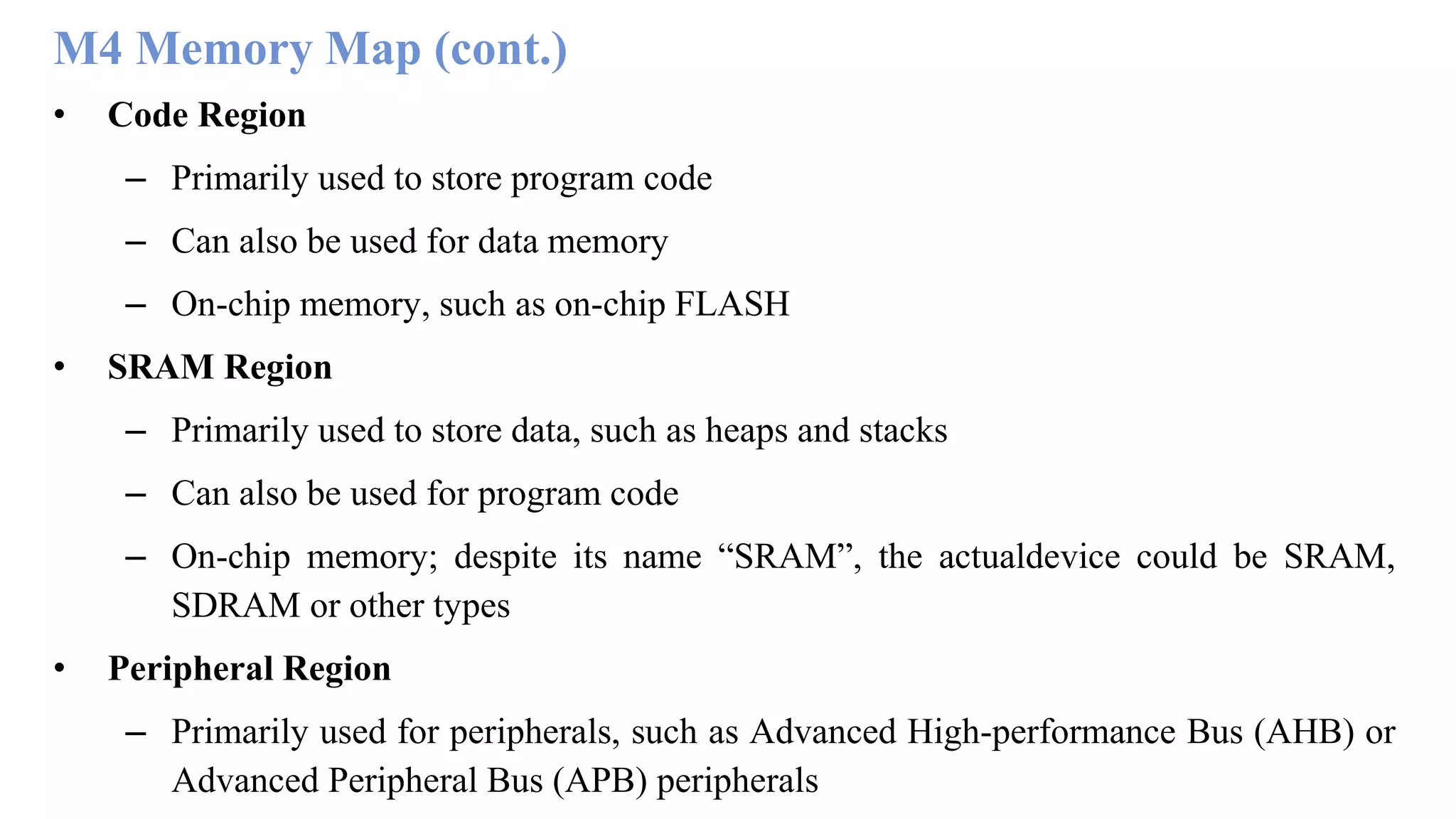
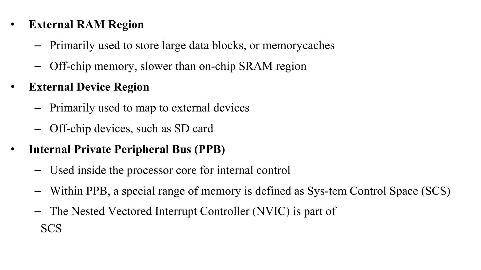
Detailed breakdown of memory regions in Cortex-M4, including code region, SRAM, peripherals, and other external/device regions.
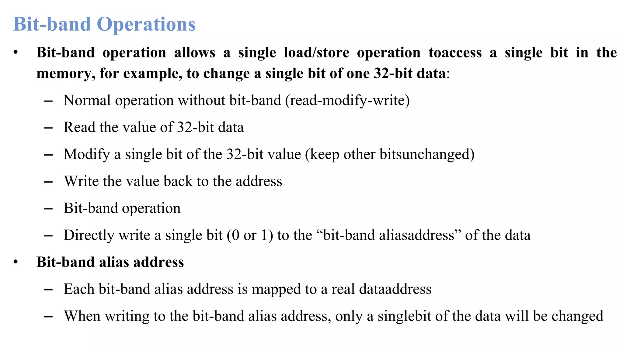
Explanation of bit-band operations that enable efficient single bit access in memory, showcasing benefits and examples.
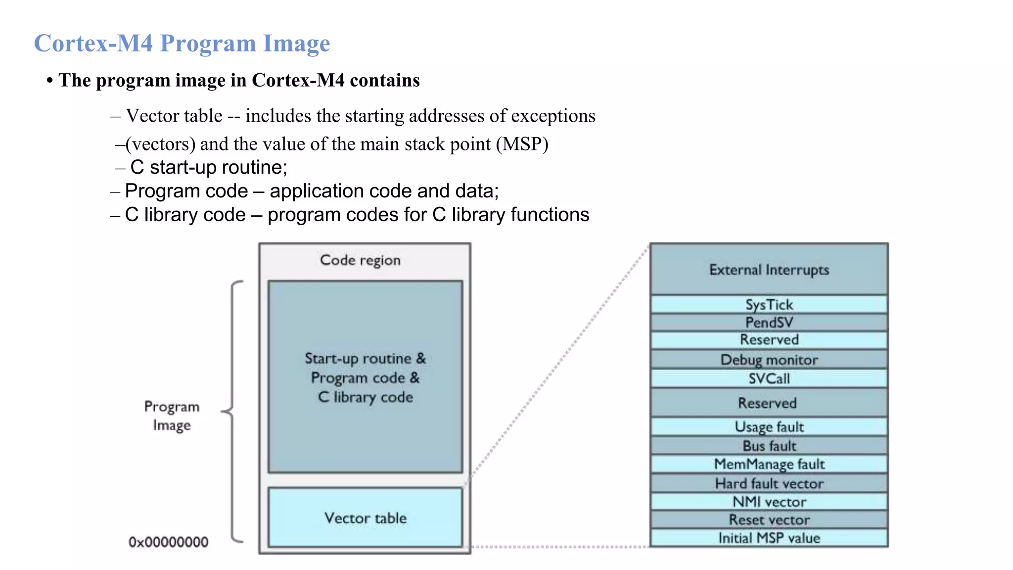
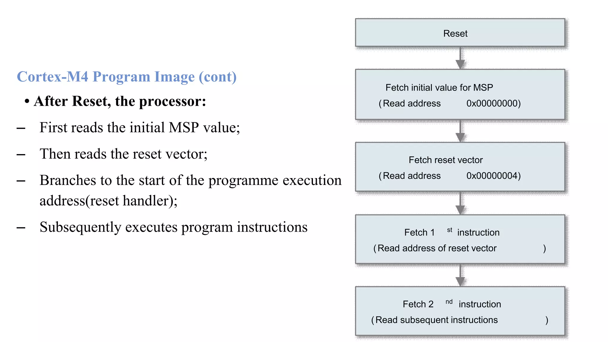
Description of the Cortex-M4 program image including vector tables, start-up routines, and program execution flow.
Cortex-M4's byte order (endianness) in memory; supports both little and big endian configurations.
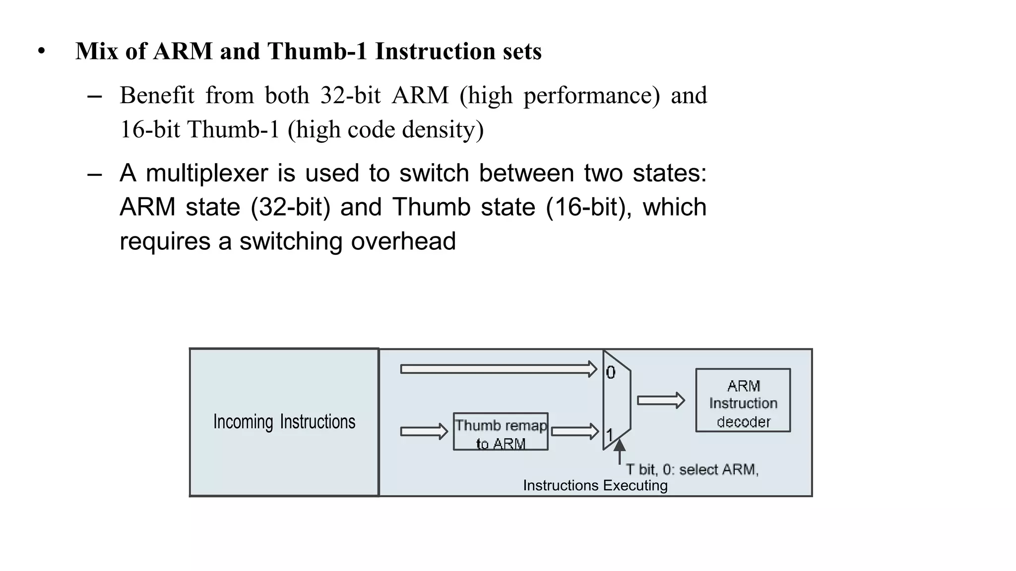
Overview of ARM and Thumb instruction sets including their characteristics, performance, and usage in Cortex-M4.
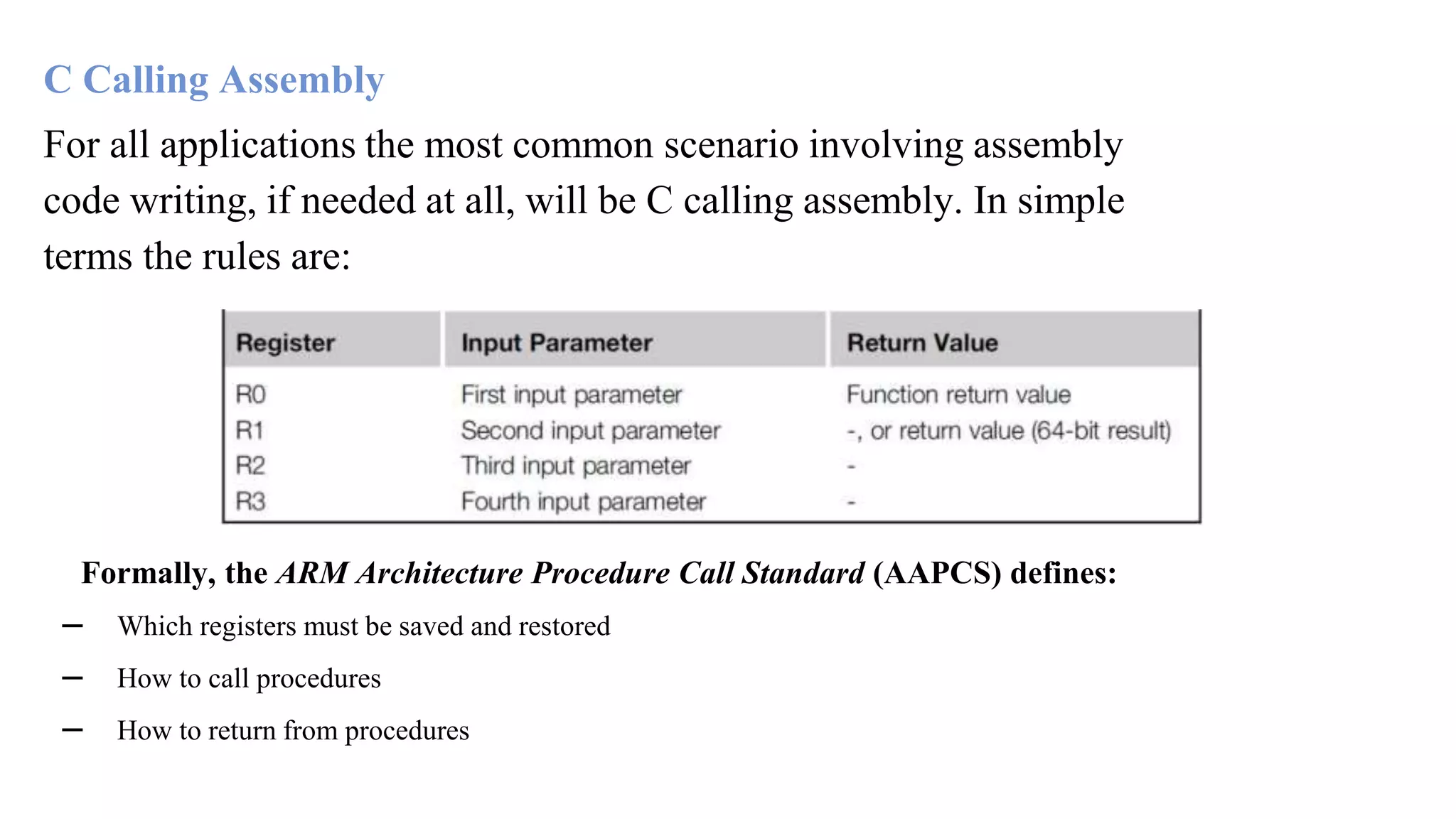
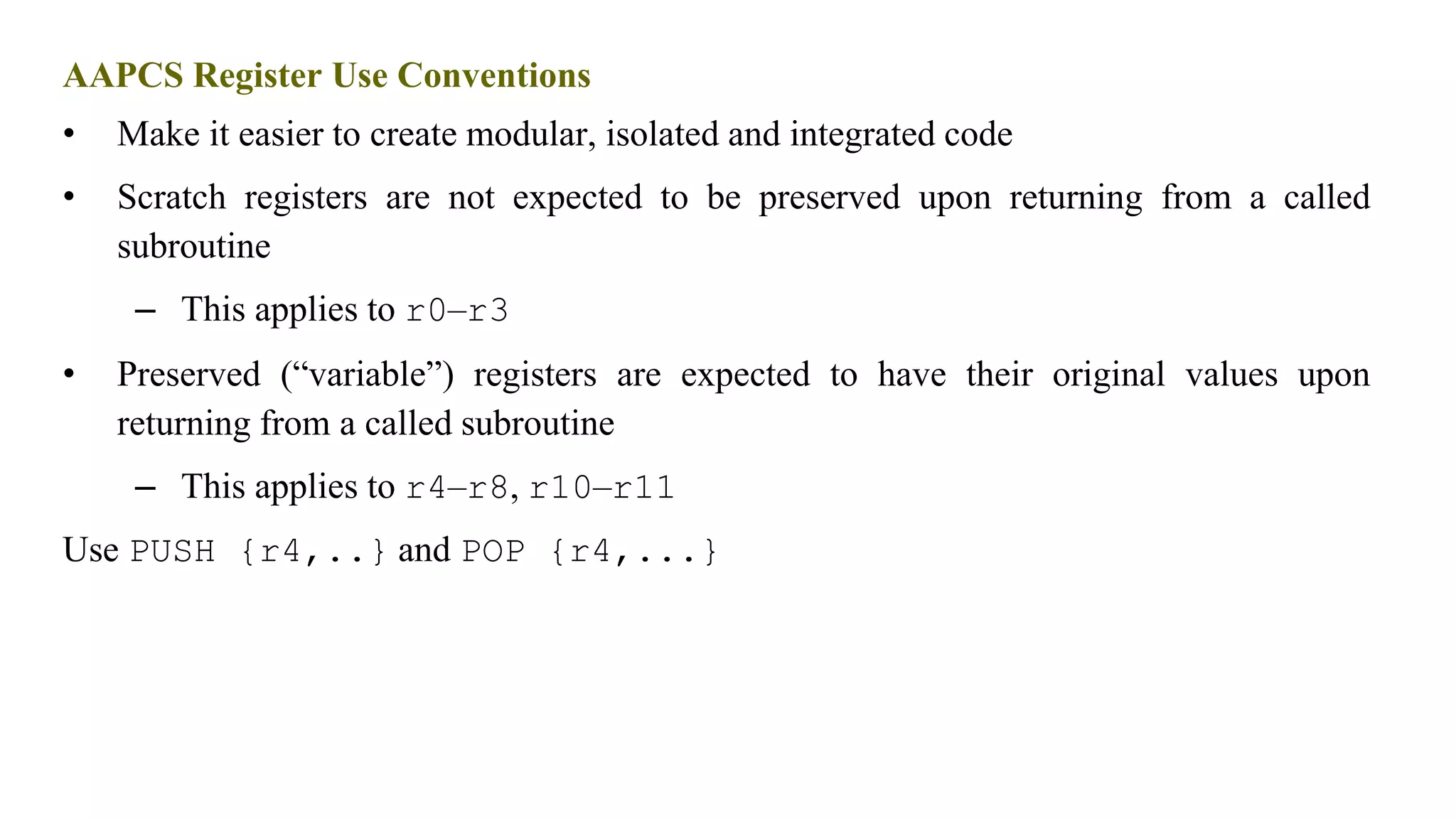
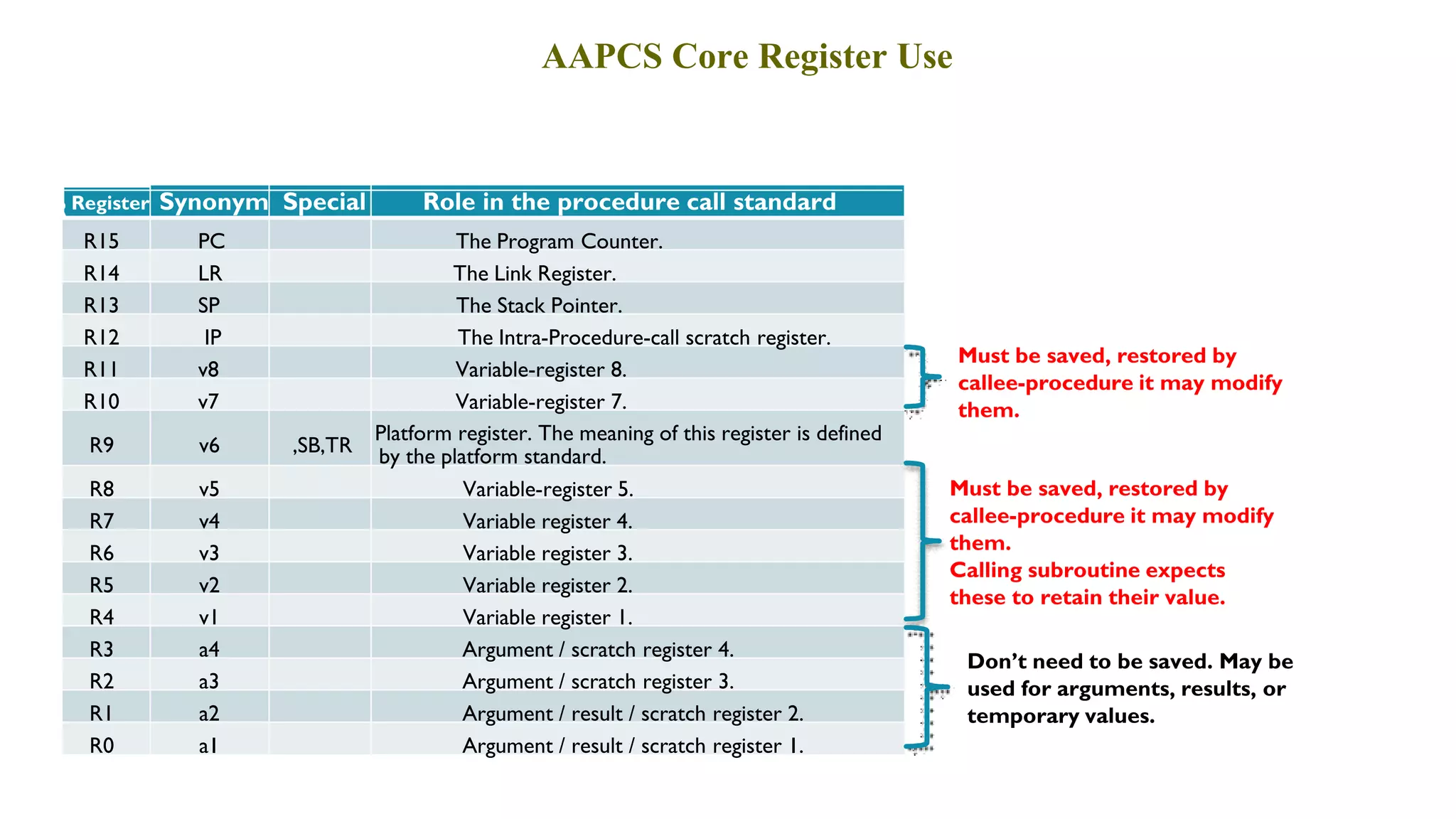
Description of C calling assembly conventions based on AAPCS, addressing register usage and subroutine calls.