Downloaded 19 times

![MU0 Instruction Set Instruction Opcode (hex) Effect LDA S 0000 (0) A := mem[S] STA S 0001 (1) mem[S] := A ADD S 0010 (2) A := A + mem[S] SUB S 0011 (3) A := A – mem[S] JMP S 0100 (4) PC := S JGE S 0101 (5) if A 0, PC := S JNE S 0110 (6) if A 0, PC := S STP 0111 (7) stop mem[S] – contents of memory location with address S Think of memory locations as being an array – here S is the array index A is the single 16 bit CPU register S is a number from instruction in range 0-4095 (000(16)-FFF(16)) LoaD A Store A ADD to A SUBtract from A JuMP Jump if Gt Equal Jump if Not Equal SToP](https://image.slidesharecdn.com/arm-190213052409/75/Introduction-to-Processor-Design-and-ARM-Processor-9-2048.jpg)

![LDA mem[100] ADD mem[101] STA mem[102] ADD R0,R1 MOV, R2, R0 ADD R2, R1, R0 1 operand (MU0) a: mem[102] b: mem[101] c: mem[100] 2 operand (AVR) a: R2 b: R1 c: R0 ADD R0,R1 ;R0:=R0+R1 MOV R0,R1 ;R0 := R1 3 operand (ARM) a: R2 b: R1 c: R0 ADD R0,R1,R2 ;R0:=R1+R2 a,b,c stored in memory REGISTORS: have e.g 8 accumulators R0-R7 a,b,c stored in registers a := b+c](https://image.slidesharecdn.com/arm-190213052409/75/Introduction-to-Processor-Design-and-ARM-Processor-20-2048.jpg)

![ARM Assembly Quick Recap MOV ra, rb MOV ra, #n ra := rb ra := n n decimal in range -128 to 127 (other values possible, see later) ADD ra, rb, rc ADD ra, rb, #n ra := rb + rc ra := rb + n SUB => – instead of + CMP ra, rb CMP ra, #n set status bits on ra-rb set status bits on ra-n CMP is like SUB but has no destination register ans sets status bits B label branch to label BL label is branch & link BEQ label BNE label BMI label BPL label branch to label if zero branch if not zero branch if negative branch if zero or plus Branch conditions apply to the result of the last instruction to set status bits (ADDS/SUBS/MOVS/CMP etc). LDR ra, label STR ra, label ADR ra, label LDR ra, [rb] STR ra, [rb] ra := mem[label] mem[label] := ra ra :=address of label ra := mem[rb] mem[rb] := ra LDRB/STRB => byte transfer Other address modes: [rb,#n] => mem[rb+n] [rb,#n]! => mem[rb+n], rb := rb+n [rb],#n => mem[rb], rb:=rb+n [rb+ri] => mem[rb+ri]](https://image.slidesharecdn.com/arm-190213052409/75/Introduction-to-Processor-Design-and-ARM-Processor-54-2048.jpg)
![MU0 to ARM Operation MU0 ARM A := mem[S] R0 := mem[S] LDA S LDR R0, S mem[S] := A mem[S] := Rn STA S STR R0, S A := A + mem[S] R0 := R0+ mem[S] ADD S LDR R1, S ADD R0, R0, R1 R0 := S n/a MOV R0, #S R0 := R1 + R2 n/a ADD R0, R1, R2 PC := S JMP S B S A R0 R1 R2](https://image.slidesharecdn.com/arm-190213052409/75/Introduction-to-Processor-Design-and-ARM-Processor-55-2048.jpg)


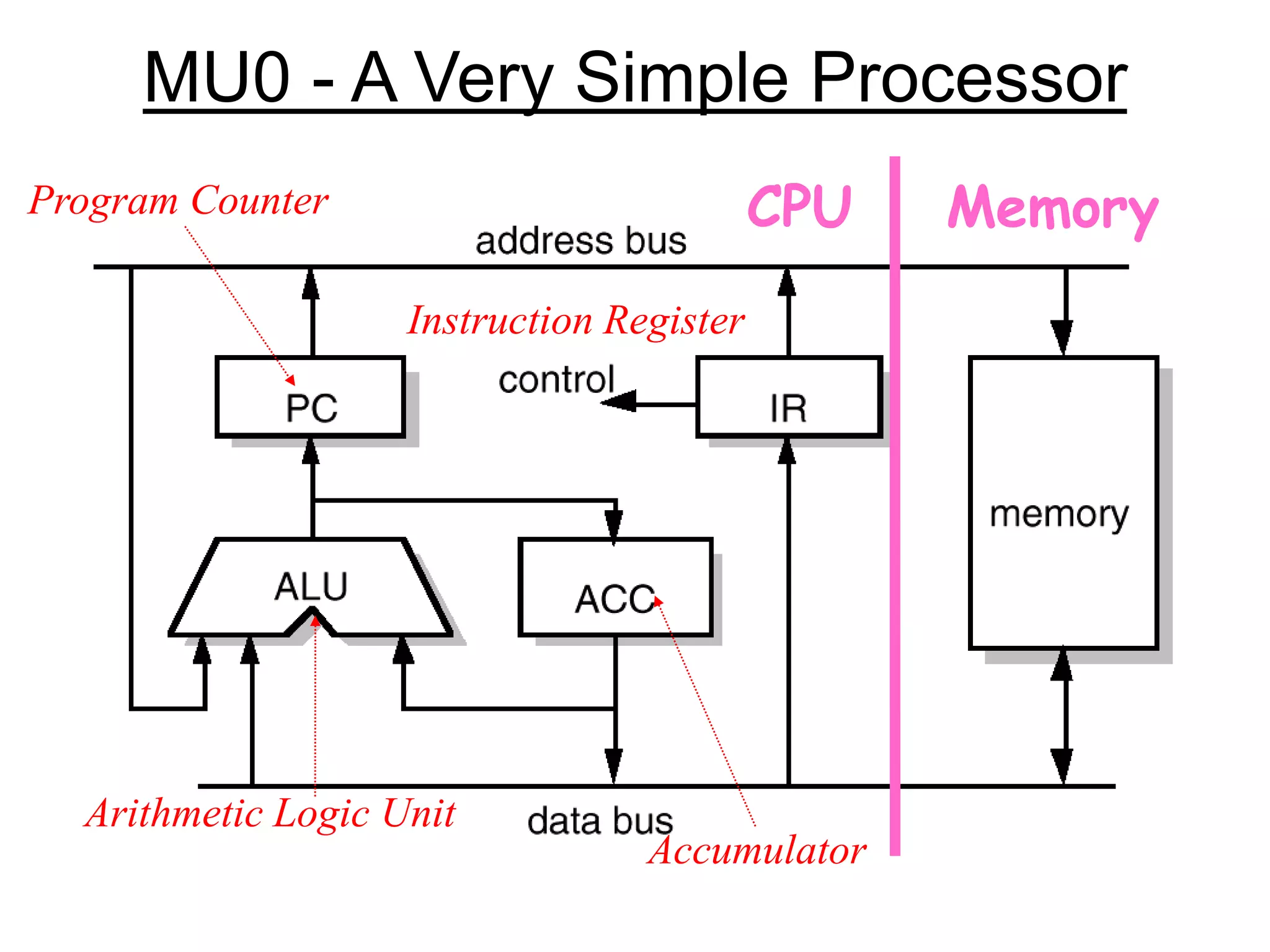
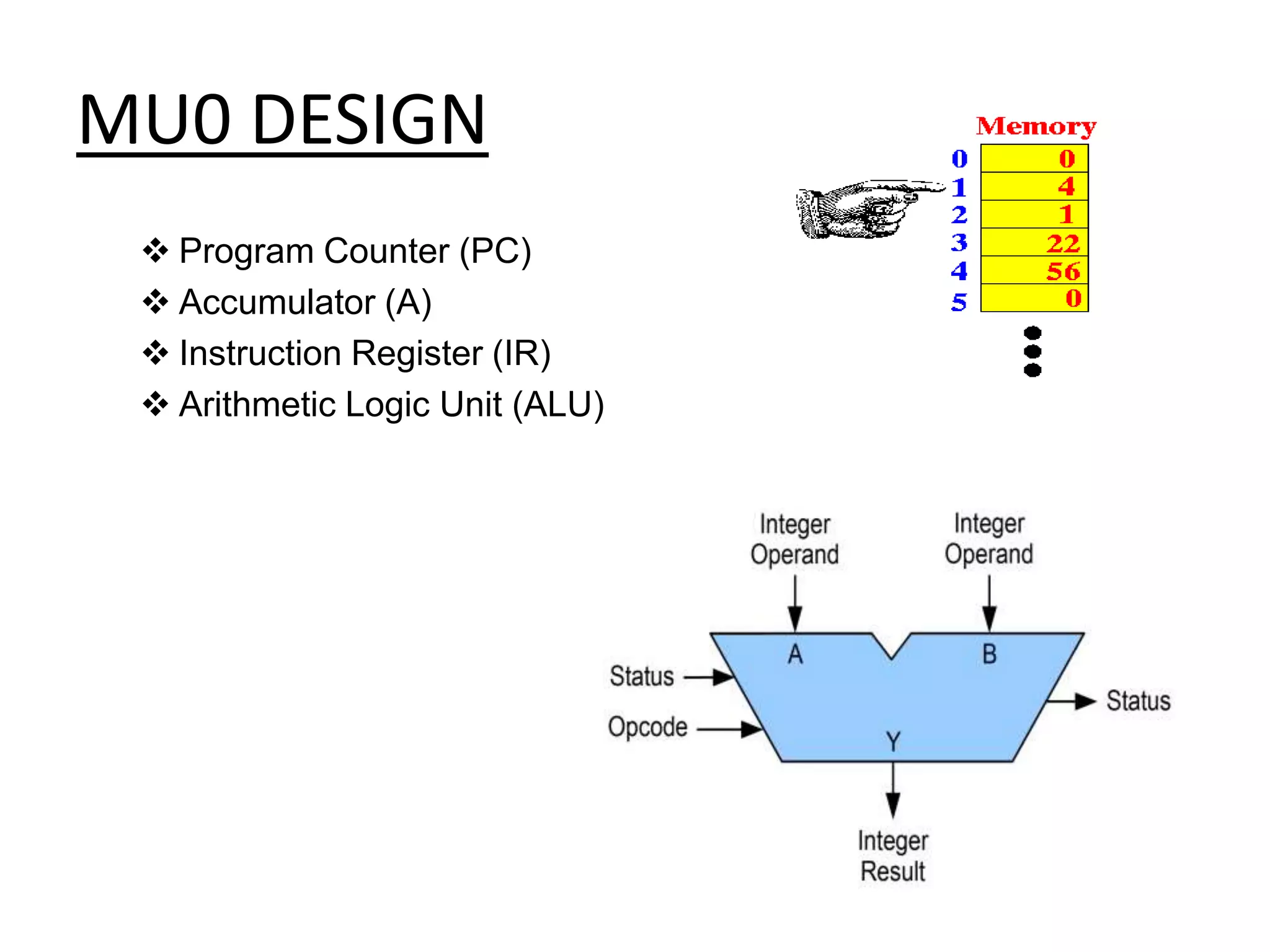
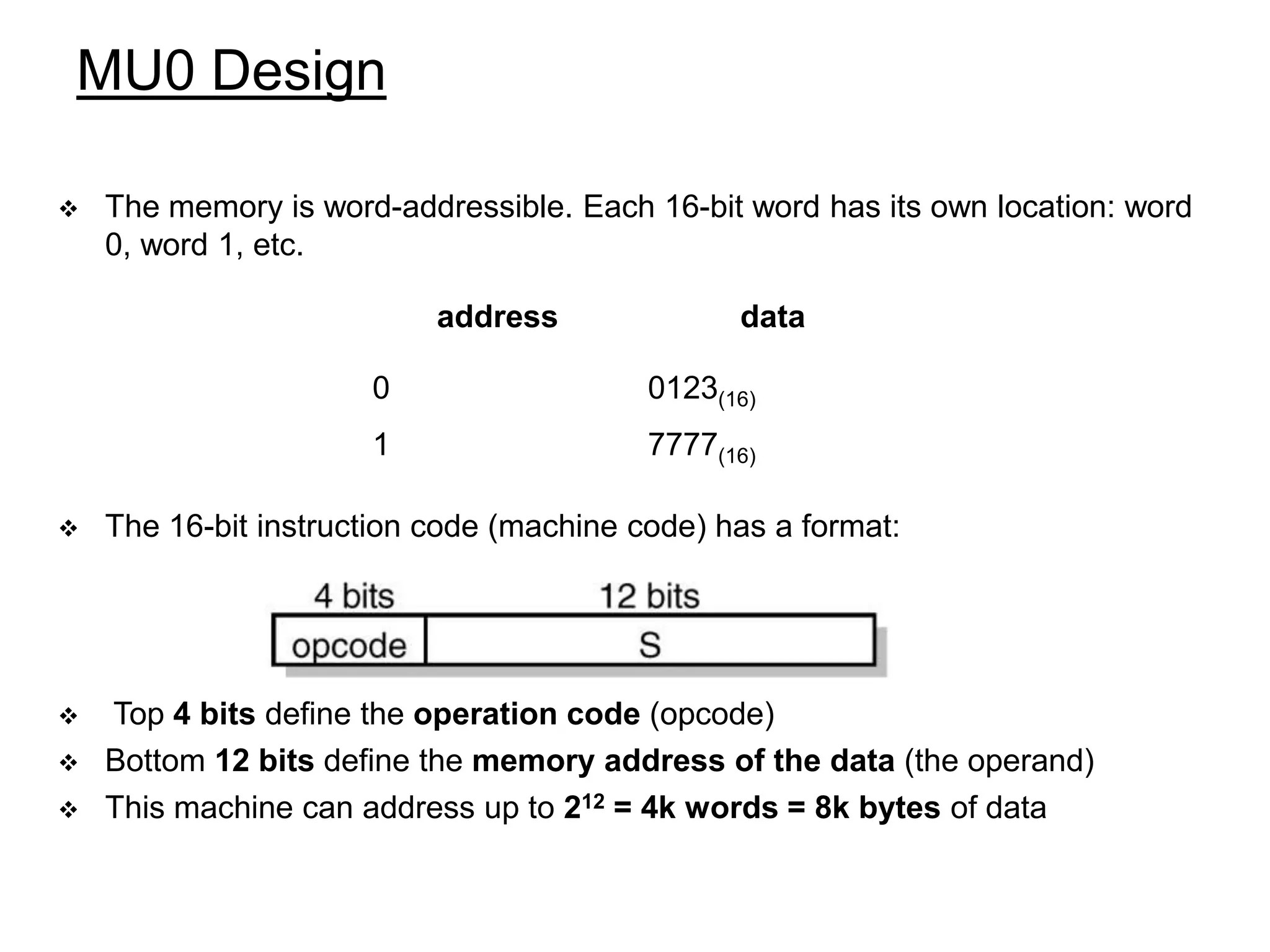
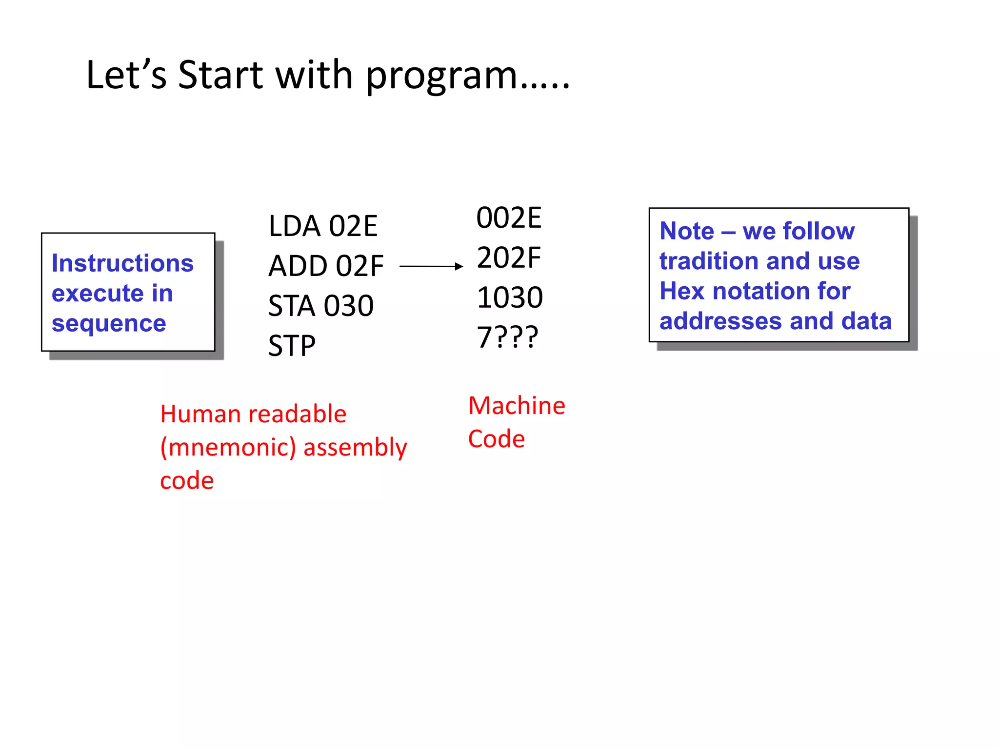
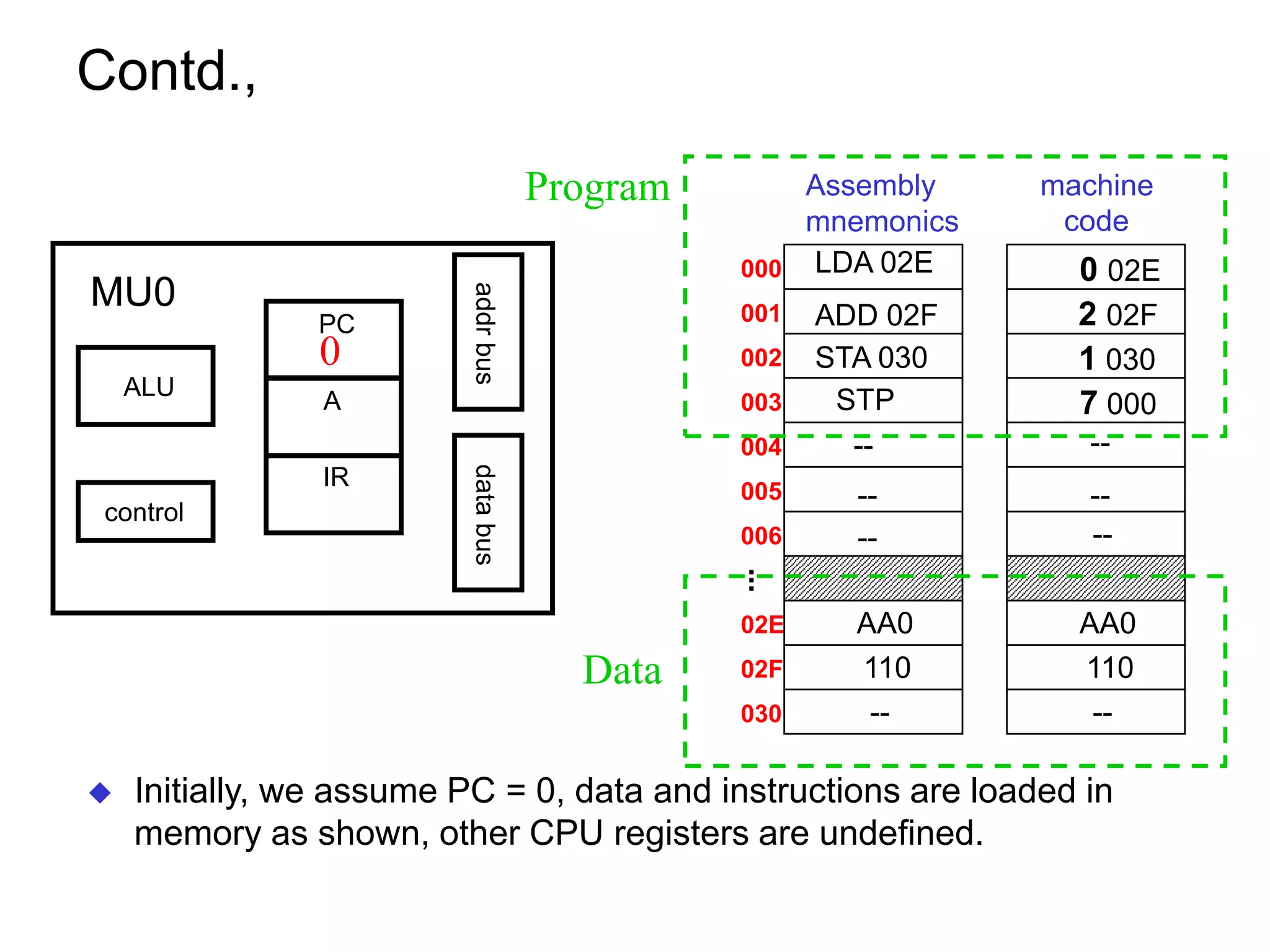
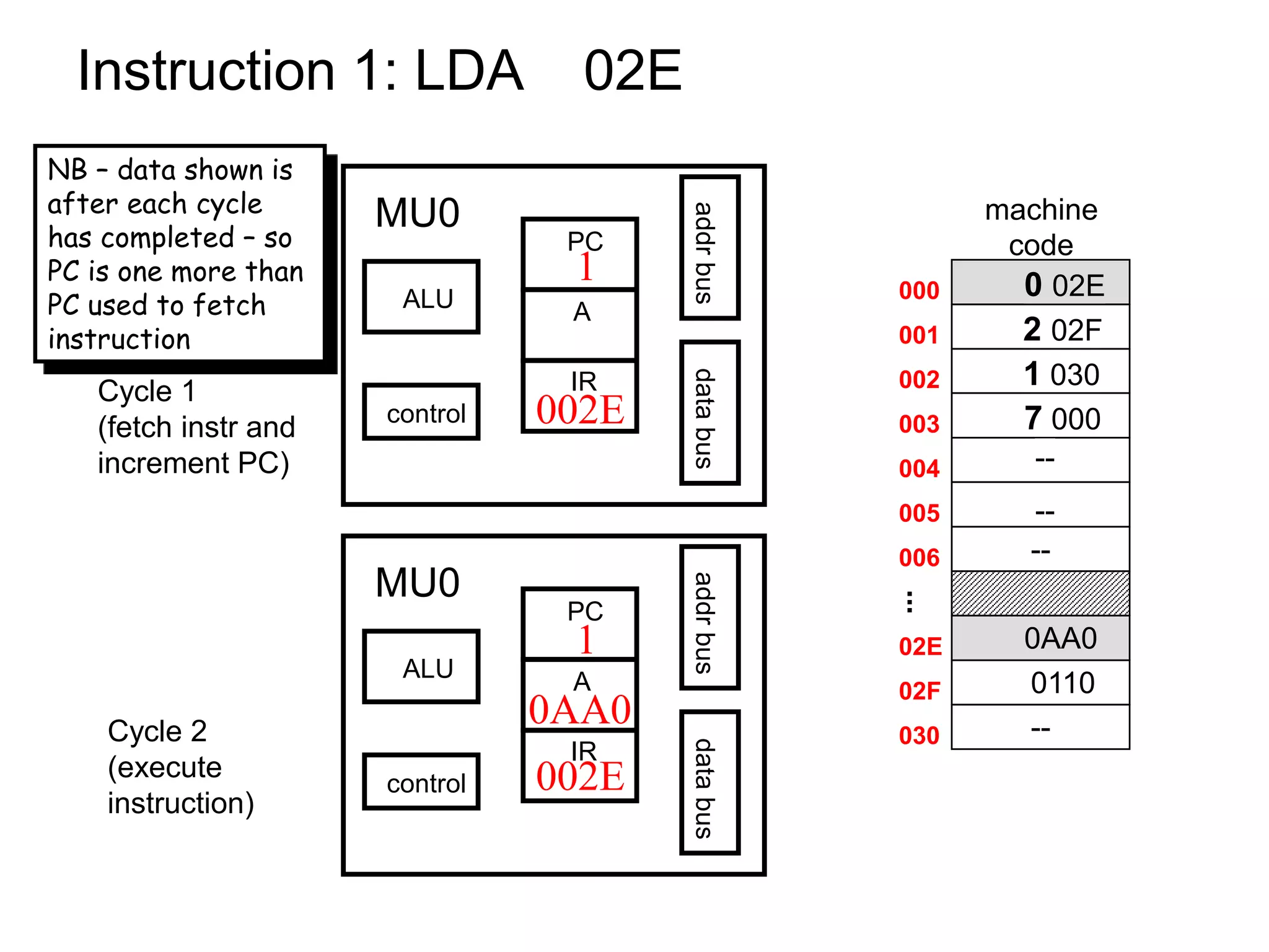
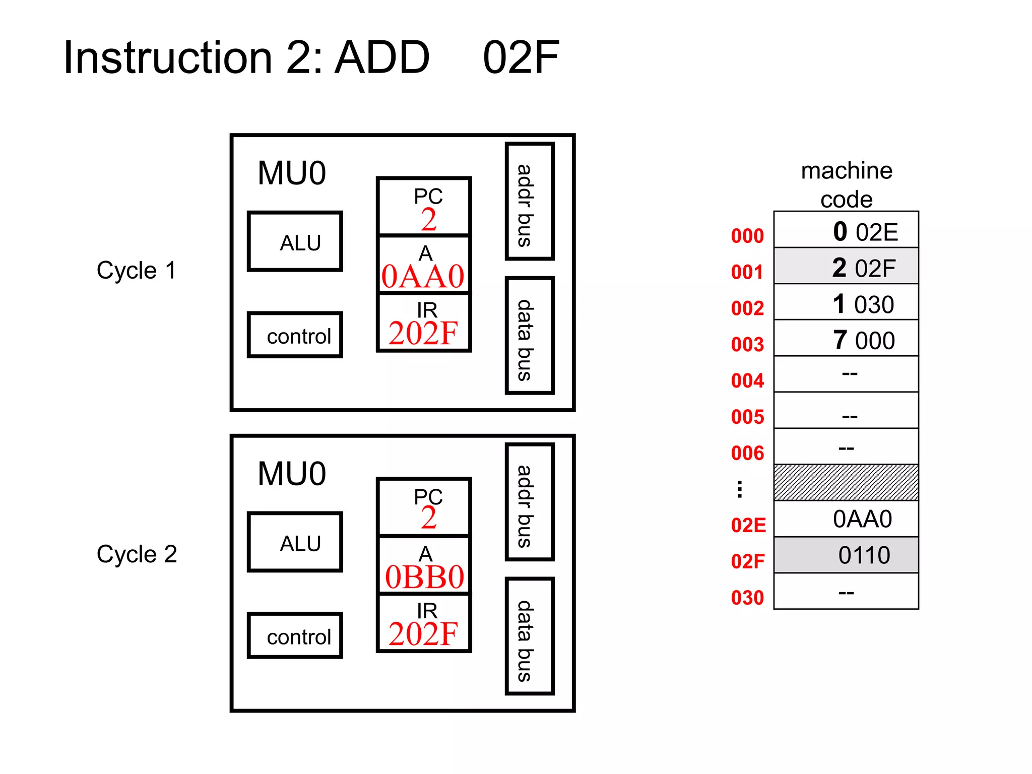
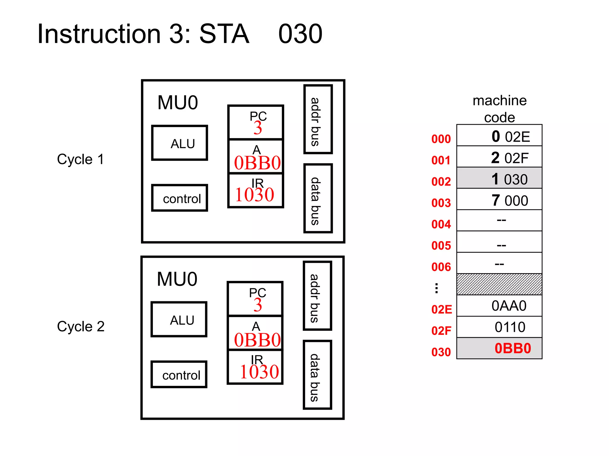
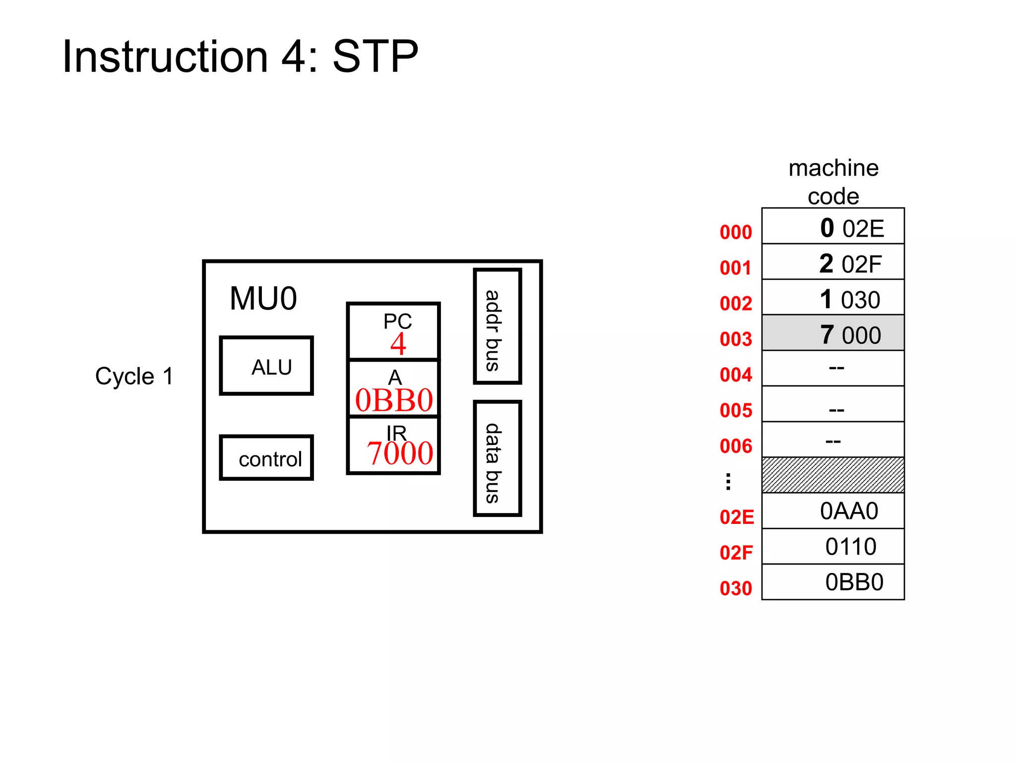
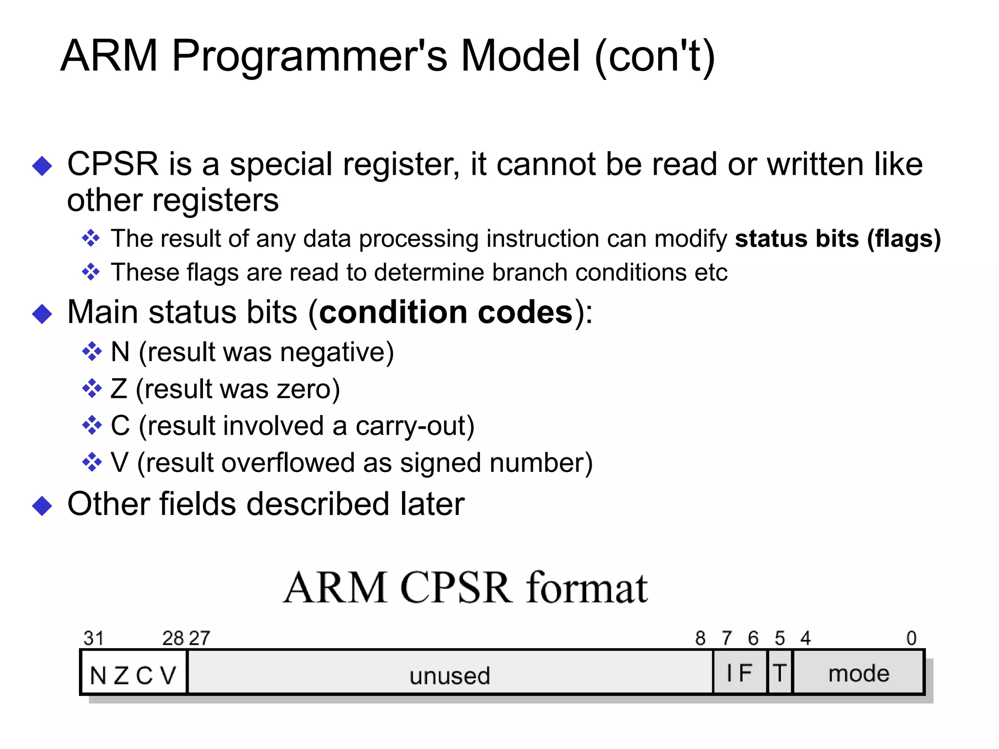
The document discusses computer architecture and the MU0 processor. It provides details on MU0's instruction set, which uses 1-address instructions and has a small set of instructions including LDA, STA, ADD, SUB, JMP, JGE, JNE, and STP. The document also explains MU0's design, which has a program counter, accumulator, instruction register, and arithmetic logic unit. It describes how MU0 executes sample instructions in a step-by-step fashion.