The document presents an enhanced architecture for ternary content addressable memory (TCAM) designed for longest prefix matching (LPM) using random access memory on field programmable gate arrays (FPGAs). It introduces an update logic that facilitates adding and deleting TCAM words, along with parallel LPM logic that significantly improves throughput by 10 times while maintaining cost-effectiveness. The proposed architecture aims to address the challenges of conventional TCAMs in terms of latency and resource usage, particularly in networking applications requiring rapid content lookup.
![TELKOMNIKA, Vol.17, No.4, August 2019, pp.1882~1889 ISSN: 1693-6930, accredited First Grade by Kemenristekdikti, Decree No: 21/E/KPT/2018 DOI: 10.12928/TELKOMNIKA.v17i4.11000 1882 Received August 28, 2018; Revised February 23, 2019; Accepted March 12, 2019 Ternary content addressable memory for longest prefix matching based on random access memory on field programmable gate array Ng Shao Kay, M. N. Marsono * School of Electrical Engineering, Faculty of Engineering, Universiti Teknologi Malaysia, 81300 Johor Bahru Malaysia *Corresponding author, e-mail: mnadzir@utm.my Abstract Conventional ternary content addressable memory (TCAM) provides access to stored data, which consists of '0', '1' and ‘don't care’, and outputs the matched address. Content lookup in TCAM can be done in a single cycle, which makes it very important in applications such as address lookup and deep-packet inspection. This paper proposes an improved TCAM architecture with fast update functionality. To support longest prefix matching (LPM), LPM logic are needed to the proposed TCAM. The latency of the proposed LPM logic is dependent on the number of matching addresses in address prefix comparison. In order to improve the throughput, parallel LPM logic is added to improve the throughput by 10× compared to the one without. Although with resource overhead, the cost of throughput per bit is less as compared to the one without parallel LPM logic. Keywords: LPM, parallel processing, TCAM, update logic Copyright © 2019 Universitas Ahmad Dahlan. All rights reserved. 1. Introduction Field-programmable gate array (FPGA) is beyond prototyping. FPGAs have been proposed in application-specific platform such as network FPGA (netFPGA) for high-throughput network processing [1, 2] such as for packet forwarding e.g. [3-5], deep packet inspection e.g. [6-8], network traffic classification e.g. [9-11], and network security e.g. [12-16]. However, conventional FPGAs do not have built-in ternary content addressable memory (TCAM). It is advantages for TCAM to be implemented in FPGAs especially for fast content look-up. TCAM on FPGA can be built based on either memory, or lookup table. UE-TCAM by Ullah [17] and Jiang [18] are examples of random-access memory (RAM) based TCAM. Both works proposed TCAM architectures with existing memory bits in FPGA. UE-TCAM [17] requires less latency compared to Jiang’s [18], although the former is without update logic. On the other hand, Jiang’s [18] consumes less memory as compared to UE-TCAM, which is suitable for RAM with narrow address width. TCAM may require frequent updates for LPM applications. Hence, UE-TCAM [17] and lookup table based TCAM such as [19] would require regeneration of partial bitfile when TCAM requires updates. In order to perform the update operation, this paper proposes an update logic to the UE-TCAM [17] architecture. The proposed update logic performs TCAM add and delete operations. To extend the application of the proposed TCAM for LPM operations, a parallel LPM logic is also proposed. Section 2 discusses in details of related works. Section 3 explains the hardware architecture for proposed update logic and parallel LPM logic. Section 4 discusses and analyzes the result. Section 5 concludes the paper. 2. Related Works Among the works that utilize RAM to implement TCAM are by Ullah et al. [17, 20, 21] where the RAM is being partitioned horizontally and vertically [17]. Divides conventional TCAM content into column and row order into L×N sub-tables, where Lis the number of horizontal partitions and N is the number of vertical partitions. Each horizontal partition (a layer) is implemented as a RAM block of the same address range. Vertical partitioning divides W-bit](https://image.slidesharecdn.com/3611000-200812054650/75/Ternary-content-addressable-memory-for-longest-prefix-matching-based-on-random-access-memory-on-field-programmable-gate-array-1-2048.jpg)
![TELKOMNIKA ISSN: 1693-6930 Ternary content addressable memory for longest prefix matching… (Ng Shao Kay) 1883 words into N sub-words of w-bit wide. The vertical partitioning is aimed to reduce the memory requirement as much as possible. In [17], an input word of C-bit wide is divided into N w-bit subwords in the vertical partitions. Hence, each RAM unit is 2 w ×K, where K is the subset of original addresses. Each subword acts as an input to the RAM unit. The overall architecture of UE-TCAM [17] consists of RAM units, ANDing logic, and layer priority encoder. Another RAM based TCAM is by Jiang [18], where narrow TCAM is used to build a wide TCAM. P narrow TCAMs are used to build N×W TCAM, and P is 1,2,..., W. The size of i-th TCAM is N×Wi where i is 1,2,..., P and W is the summation of Wi. The lookup time of P RAMs is O(1) time. The update time will be determined by the longest time of update for RAM or O(2 w ) time [18]. Stated when the depth of each RAM is 2 (w=1) or 4 (w=2), the overall memory requirement is at its minimum. Simple dual-port RAM is being used to reduce update latency to 2 w +1 cc. Another work [22] focused on investigating different SRAM-based structure for IP look-up by the Jiang and Prasanna. A modular architecture which consists of arrays of small-size RAM-based TCAM was also shown in [18]. The modular architecture is mainly to improve throughput and resource usage especially for large-scale implementation that has complex routing from bitwise ANDing and priority encoding, thus reducing the throughput. Besides, the achievable clock rate is also affected. Resource sharing is achieved by decoupling update logic to be shared by multiple TCAM units. Each unit is pipelined to solve for the throughput degradation in ANDing large number of bit-vectors. Low power RAM-based hierarchical CAM [23] was also introduced to reduce power from the modular architecture which constructed from P-narrow TCAM. Several other worthy approaches can be found in [24, 25]. 3. Proposed RAM-based TCAM for Longest Prefix Matching In the UE-TCAM architecture, C-bit input data is sent to L number of layers which contain N vertical partitions in each layer (i.e., N w-bit subwords). The result of the vertical partition is K-bit, which is the subset of original address. Each bit of K-bit represents the original matching address of the TCAM. The K-bit addresses is then subjected through layer priority encoder (LPE). The lowest matching address serves as the possible match address (PMA). The CAM priority encoder (CPE) selects the lowest PMA as the final match address (MA). Increasing data width of a TCAM can be done through increasing either the number of partitions in each layer or the depth of the RAM. On the other hand, increasing the number of words stored in TCAM can be done by increasing either the width of RAM in every partition or increasing the number of layers. 3.1. Proposed Update Logic There are two types of operations in the proposed TCAM architecture; lookup operation and update operation. The lookup operation is where input data sent to the TCAM to produce the output address. On the other hand, the update operation consists of the add and delete operations. The add operation adds TCAM word to certain addresses, whereas the delete operation deletes TCAM word from certain addresses. The lookup operation takes 1 clock cycle (cc), whereas the update operations take 2 w +1 cc. To add the update logics to the existing UE-TCAM architecture, several blocks are added, which are dataRegUnit, maskUnit, and updateLogic. The overall architecture is shown in Figure 1. The dataRegUnit is to hold the input data for update operations that take many cycles. The maskUnit decodes the mask for the add operation. MaskUnit will have N number of maskProcessUnit. The i-th bit of mask is ‘1’ if the i-th bit of ternary word is binary or ‘0’ if the i-th bit of ternary word is ‘don't care’ or usually denoted as ‘X’, e.g., ‘10XX’ is masked by ‘1100’. The maskUnit will take C-bit mask, data, and update address counter from updateLogic to produce the update address and wren flag for the RAM in each vertical partition. For LPM application, the ‘X’ or ‘0’ are located in the lowest i significant bits. In networking, the netmask is divided into two portions; the higher network prefix and the lower host suffix. The network prefix bits contain only '1' in netmask and are used for IP address forwarding. In the maskUnit, the bit that is high or not ‘X’ in the mask will be ANDed with C-bit data, whereas the bit that is ‘0’ or ‘X’ is inverted and ANDed with the update address counter from the updateLogic. Then the ANDed results are both ORed together to become a valid update address for each vertical partition. By doing so, data are translated to the update](https://image.slidesharecdn.com/3611000-200812054650/75/Ternary-content-addressable-memory-for-longest-prefix-matching-based-on-random-access-memory-on-field-programmable-gate-array-2-2048.jpg)
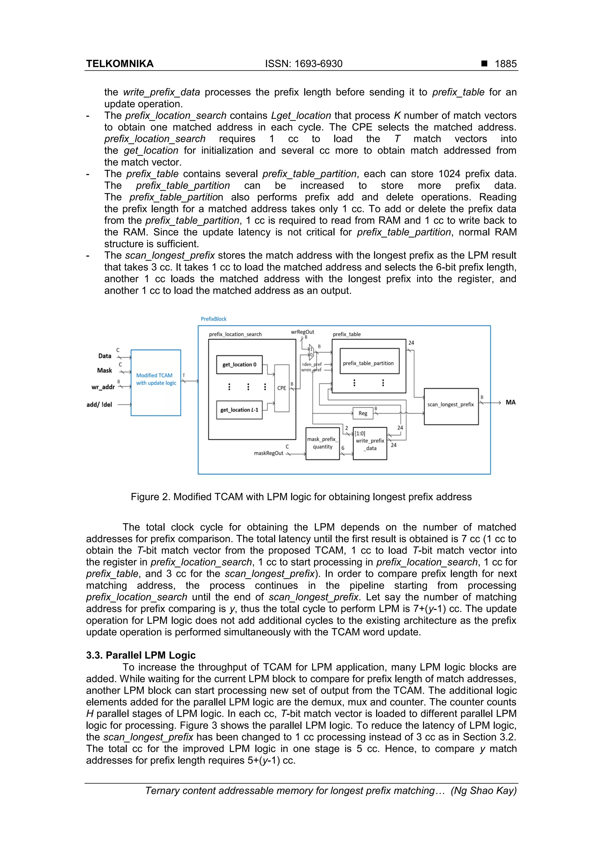
![ ISSN: 1693-6930 TELKOMNIKA Vol. 17, No. 4, August 2019: 1882-1889 1884 address of the vertical partition. If there is an ‘X’ in the mask, one or more addresses of the vertical partition or the location inside RAM will be updated. The wr_addr is the word address for writing to the TCAM. There is a decoder in updateLogic, which functions for decoding the write address into bit location m of K-bit data for RAM update. For example, when the write address is 111, the 7-th bit of K-bit output of the decoder will be ‘1’. There are two decoded data from the updateLogic to write to the RAM partition, one is for the add operation and another is for the delete operation. One-hot encoding output from updateLogic is sent to Control Unit (CU) to control the write enabling of the dedicated layer. The update address counter in updateLogic counts from 0 to 2 w -1. As the count is w-bit, concatenating N number of w-bit counts become C-bit update address counter. The C-bit update address is sent to maskUnit for processing, which returns the write address for RAM. During the add operation, only certain location of the RAM will need to be updated, whereas during delete operation, all RAM locations will be updated. Every vertical partition is made of a simple dual-port RAM. Each bit stored in RAM represents a TCAM location. As every RAM is K-bit wide, each RAM stores K-bit TCAM location. As the update operation will only update m-th bit without overwriting the remaining K-1 bits, the RAM performs read for one cycle and performs write (of a new K-bit data) in another cycle. By using dual-port RAM, read and write operations can be done simultaneously in one cc. Hence, the total cycle for updating the RAM is 2 w +1 cc. When no update operation is performed, the data input of TCAM will be the input to TCAM for the lookup operation. Figure 1. Modified UE-TCAM [17] with added update logic 3.2. Proposed LPM Logic The proposed LPM logic for LPM application is shown in Figure 2. The modified TCAM with added update logic is as in Figure 1, except the LPE and CPE are removed. The K-bit output from each layer is concatenated to become the total match vector of T bits. The total match vector is then sent to prefix_block for extracting the prefix length for each match address. The prefix_location_search functions to obtain one match address starting from a lower address at each cycle. The match address from prefix_location_search is sent to prefix_table to obtain the prefix length of the matched address. After extracting the prefix length for each matched address, the scan_longest_prefix determines the longest prefix hit as the LPM result. - The mask_prefix_quantity and the write_prefix_data are for the prefix length update. The mask_prefix_quantity calculates the total number of prefix length, while](https://image.slidesharecdn.com/3611000-200812054650/75/Ternary-content-addressable-memory-for-longest-prefix-matching-based-on-random-access-memory-on-field-programmable-gate-array-3-2048.jpg)
![ ISSN: 1693-6930 TELKOMNIKA Vol. 17, No. 4, August 2019: 1882-1889 1888 4.2. Comparison with Previous Works There are two major works on RAM-based TCAM built on FPGA being compared to this work, which are [17,18]. The difference is that [18] was built with narrow TCAMs whereas UE-TCAM was built with large RAM blocks. The proposed TCAM for LPM application cannot be directly compared with the existing works [17,18] because their works were implemented on different FPGA families. Thus, UE-TCAM is built on the targeted Cyclone IV FPGA in this work. Table 1 shows the comparison with previous works. The UE-TCAM built has a maximum frequency of 179.28 MHz and latency of 3 cc. When update logic and LPM application are added, the frequency becomes 126.66 MHz with 12 cycle latency. When parallel LPM logic is added to the TCAM, the frequency decreases to 106.52 MHz at 10 cc latency due to additional logic added for controlling parallel LPM logic. Table 1. Comparison with Existing Works 5. Conclusion In this paper, a RAM-based TCAM is proposed on targeted FPGA based on the UE-TCAM architecture [17]. An update logic has been added for performing the update operations. Parallel LPM logic has been proposed with improved throughput for LPM application. In the proposed TCAM, the lookup latency depends the number of matching addresses for prefix comparison. Apart from the proposed TCAM architecture for LPM application, there is still some rooms for improvement. The TCAM architecture can be divided into different blocks to store for contents according to prefix length. Doing so could reduce the processing time of the LPM logic. A smaller number of matching vectors will be processed by LPM logic. Data of different prefix length could be stored with RAM block of different sizes to reduce the overall memory size for building TCAM. This concept is about similar to the DR-TCAM in [26]. Lastly, depending on the TCAM application, the input data could be compressed before being stored in RAM block to further reduce TCAM memory usage. References [1] Lockwood JW, McKeown N, Watson G, Gibb G, Hartke P, Naous J, Raghuraman R, Luo J. NetFPGA--an open platform for gigabit-rate network switching and routing. Proceedings of the 2007 IEEE International Conference on Microelectronic Systems Education (MSE'07), San Diego, 2007: 160-161. [2] Zilberman N, Audzevich Y, Kalogeridou G, Manihatty-Bojan N, Zhang J, Moore A. NetFPGA: Rapid prototyping of networking devices in open source. ACM SIGCOMM Computer Communication Review. 2015; 45(4): 363--364. [3] Srinivasan V and Varghese G. Fast address lookups using controlled prefix expansion. ACM Transactions on Computer Systems (TOCS), 1999; 17(1): 1–40. [4] Kobayashi M, Murase T. and Kuriyama A. A longest prefix match search engine for multi-gigabit IP processing. Proceedings of the 2000 IEEE International Conference on Communications (ICC 2000). New Orleans. 2000: 1360–1364. [5] Li W, Li X, Li H. MEET-IP: Memory and energy efficient TCAM-based IP lookup. Proceedings of the 2017 26th International Conference on Computer Communication and Networks (ICCCN). Vancouver. 2017: 1-8.](https://image.slidesharecdn.com/3611000-200812054650/75/Ternary-content-addressable-memory-for-longest-prefix-matching-based-on-random-access-memory-on-field-programmable-gate-array-7-2048.jpg)
![TELKOMNIKA ISSN: 1693-6930 Ternary content addressable memory for longest prefix matching… (Ng Shao Kay) 1889 [6] Yang J, Jiang L, Bai X, Peng H, Dai Q. A High-Performance Round-Robin Regular Expression Matching Architecture Based on FPGA. Proceedings of the 2018 IEEE Symposium on Computers and Communications (ISCC). Natal. 2018: 1--7. [7] Jayashree S and Shivashankarappa N. Deep packet inspection using ternary content addressable memory. Proceedings of the 2014 International Conference on Circuits, Communication, Control and Computing (I4C), Bangalore. 2014: 441–447. [8] Yang J, Jiang L, Bai X, Dai Q. High Performance Regular Expression Matching on FPGA. Proceedings of the 2017 International Conference on Collaborative Computing: Networking, Applications and Worksharing. Edinburgh. 2017: 541--553. [9] Wang K. and Hengkui W. TCAM-PC: Space-efficient TCAM-based packet classification with packet- forwarding-rate constraints. Proceedings of the 12th IEEE International Conference on Electronic Measurement & Instruments (ICEMI). Qingdao. 2015. 1:260–264. [10] Qu YR, Prasanna VK. High-performance and dynamically updatable packet classification engine on FPGA. IEEE Transactions on Parallel and Distributed Systems. 2016; 27(1): 197-- 209. [11] Zerbini CA, Finochietto JM. Performance evaluation of packet classification on FPGA-based TCAM emulation architectures. Proceedings of the 2012 IEEE Global Communications Conference (GLOBECOM). Anaheim. 2012: 2766—2771. [12] Nakahara H, Sasao T, Matsuura M, Kawamura Y. The parallel sieve method for a virus scanning engine. Proceedings of the 2009 12th IEEE Euromicro Conference on Digital System Design, Architectures, Methods and Tools (DSD 2009). Patras. 2009: 809--816. [13] Aldwairi M, Flaifel Y, Mhaidat K. Efficient Wu-Manber pattern matching hardware for intrusion and malware detection. Proceedings of the 2018 IEEE International Conference on Electrical, Electronics, Computers, Communication, Mechanical and Computing (EECCMC). Vellore. 2018. [14] Onizawa N, Gross WJ, Hanyu T. A low-energy variation-tolerant asynchronous TCAM for network intrusion detection systems. Proceedings of the IEEE 19th International Symposium on Asynchronous Circuits and Systems (ASYNC), Santa Monica. 2013: 8–15. [15] Ricart-Sanchez R, Malagon P, Alcaraz-Calero JM, Wang Q. Hardware-Accelerated Firewall for 5G Mobile Networks. Proceedings of the IEEE 26th International Conference on Network Protocols (ICNP). Cambridge. 2018: 446--447. [16] Nakamura Y, Sawaguchi S, Nishi H. Implementation and evaluation of an FPGA-based network data anonymizer. IEEJ Transactions on Electrical and Electronic Engineering. 2017; 12: S134--40. [17] Ullah Z, Jaiswal MK, Cheung RC, So HK. UE-TCAM:An ultra efficient SRAM-based TCAM. Proceedings of the 2015 IEEE Region 10 Conference (TENCON 2015). Macau. 2015: 1--6. [18] Jiang W. Scalable ternary content addressable memory implementation using FPGAs. Proceedings of the 2013 ACM/IEEE Symposium on Architectures for Networking and Communications Systems (ANCS). San Jose. 2013; 71–82. [19] Hager S, Bendyk D, Scheuermann B. Partial reconfiguration and specialized circuitry for flexible FPGA-based packet processing. Proceedings of the 2015 International Conference on ReConFigurable Computing and FPGAs (ReConFig). Riviera Maya. 2015; 1--6. [20] Ullah Z, Jaiswal MK, Cheung RC. E-TCAM: an efficient SRAMbased architecture for TCAM. Circuits, Systems, and Signal Processing. 2014; 33(10): 3123–3144 [21] Ullah Z, Ilgon K, Baeg S. Hybrid Partitioned SRAM-Based Ternary Content Addressable Memory. IEEE Transactions on Circuits and Systems I. 2012; 59(12): 2969–2979. [22] Jiang W, Prasanna VK. Data structure optimization for power-efficient IP lookup architectures. IEEE Transactions on Computers. 2013; 62(11): 2169--2182. [23] Qian Z, Margala M. Low power RAM-based hierarchical CAM on FPGA. Proceedings of the 2014 International Conference on ReConFigurable Computing and FPGAs (ReConFig). Cancun. 2014; 1–4. [24] Ahmed A, Park K, Baeg S. Resource-efficient SRAM-based ternary content addressable memory. IEEE Transactions on Very Large Scale Integration (VLSI) Systems. 2017; 25(4):1583--7. [25] Huang K, Chen X. A power-efficient approach to TCAM-based regular expression matching. Proceedings of the 27th IEEE International Conference on Computer Communication and Networks (ICCCN). Hangzhou. 2018: 1-9. [26] Yang BD. Low-Power Effective Memory-Size Expanded TCAM Using Data-Relocation Scheme. IEEE Journal of Solid-State Circuits. 2015; 50(10): 2441–2450.](https://image.slidesharecdn.com/3611000-200812054650/75/Ternary-content-addressable-memory-for-longest-prefix-matching-based-on-random-access-memory-on-field-programmable-gate-array-8-2048.jpg)