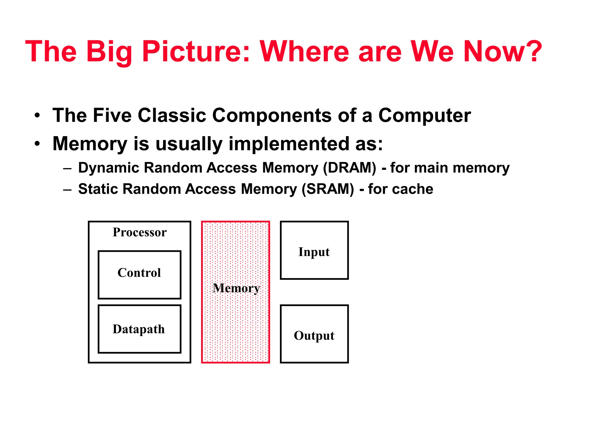
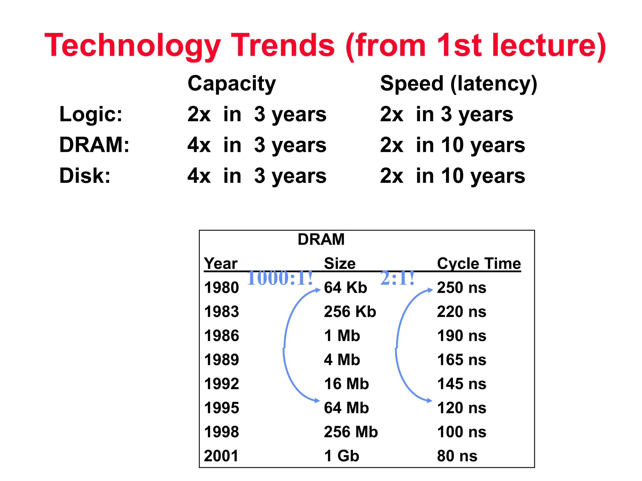
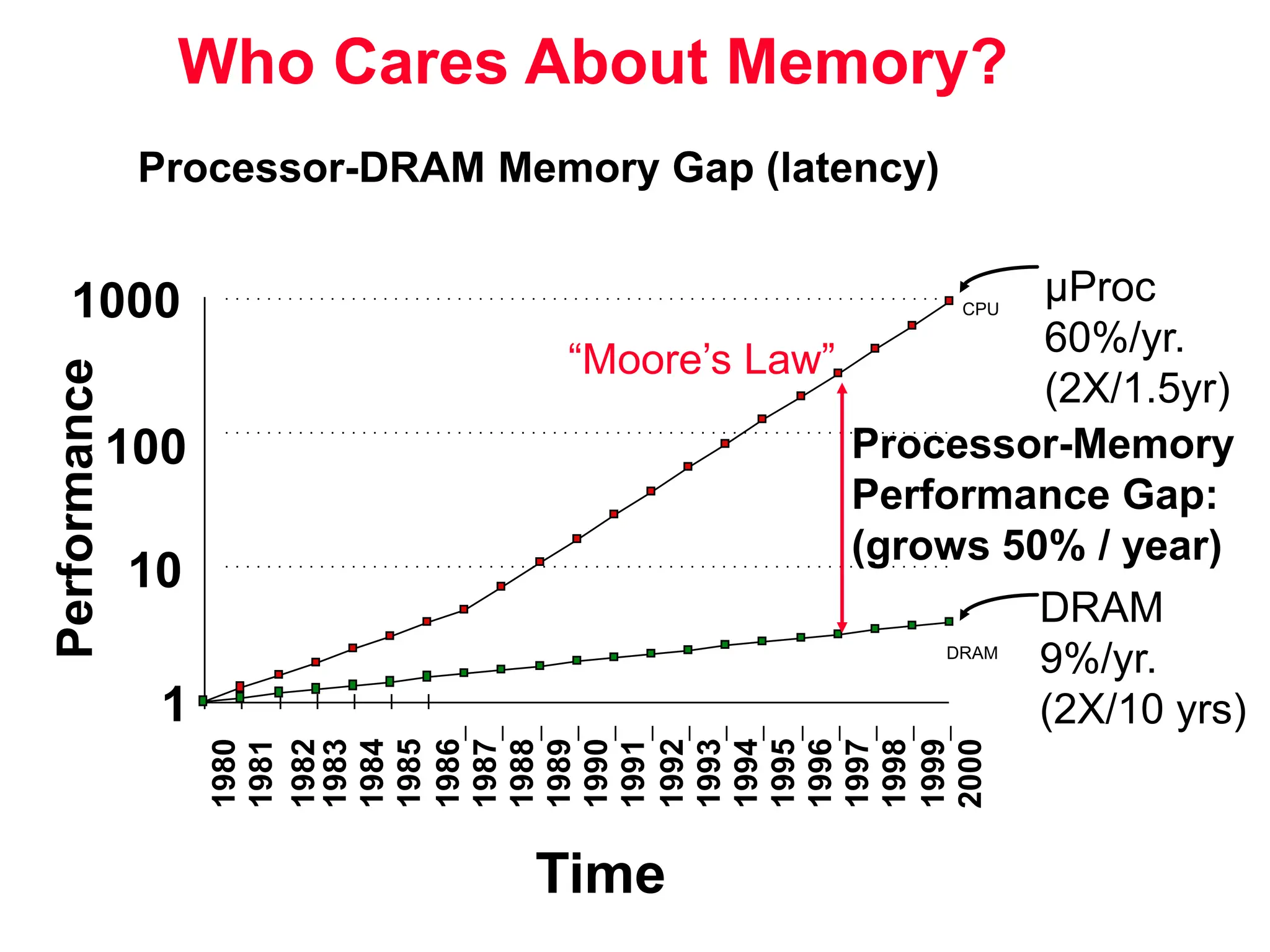
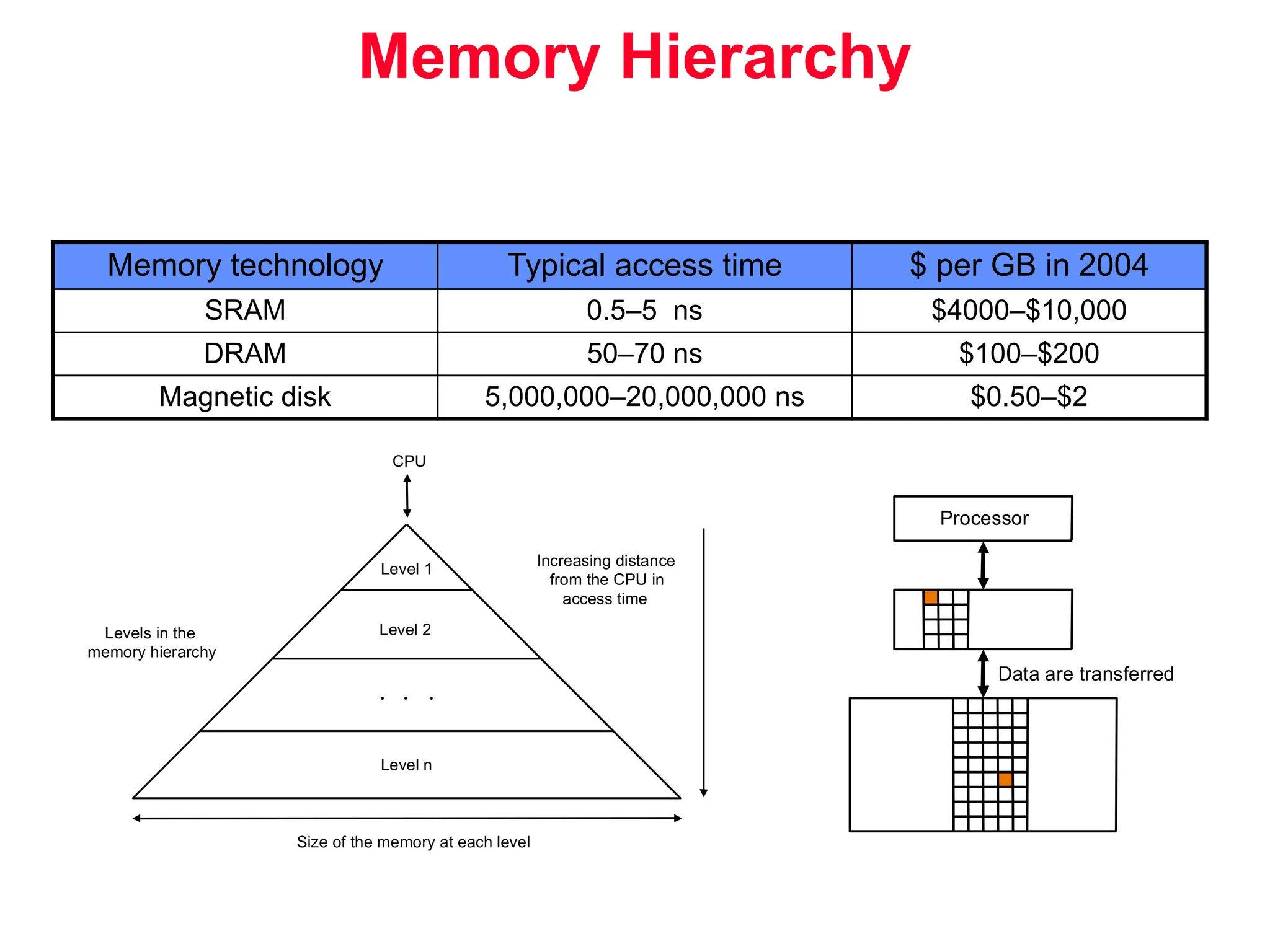
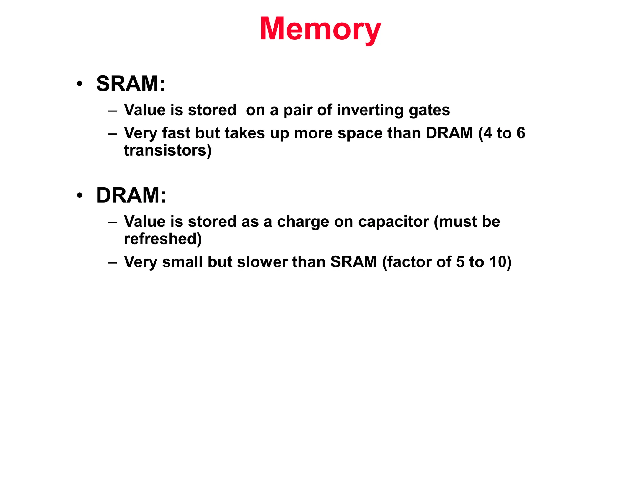
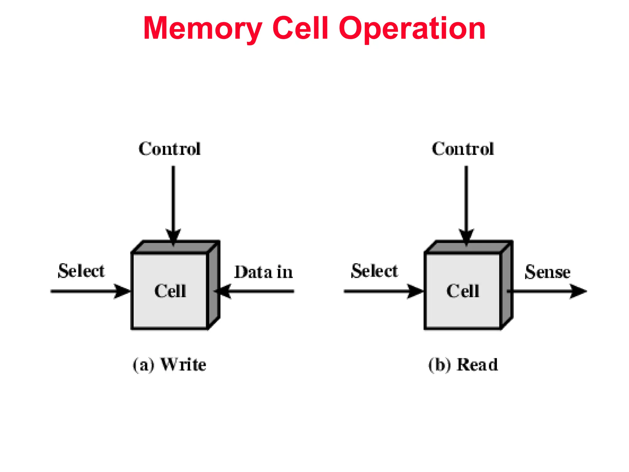
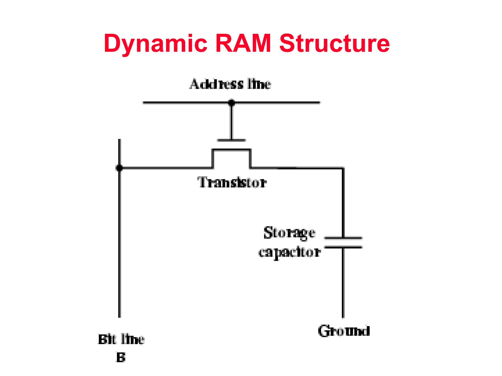
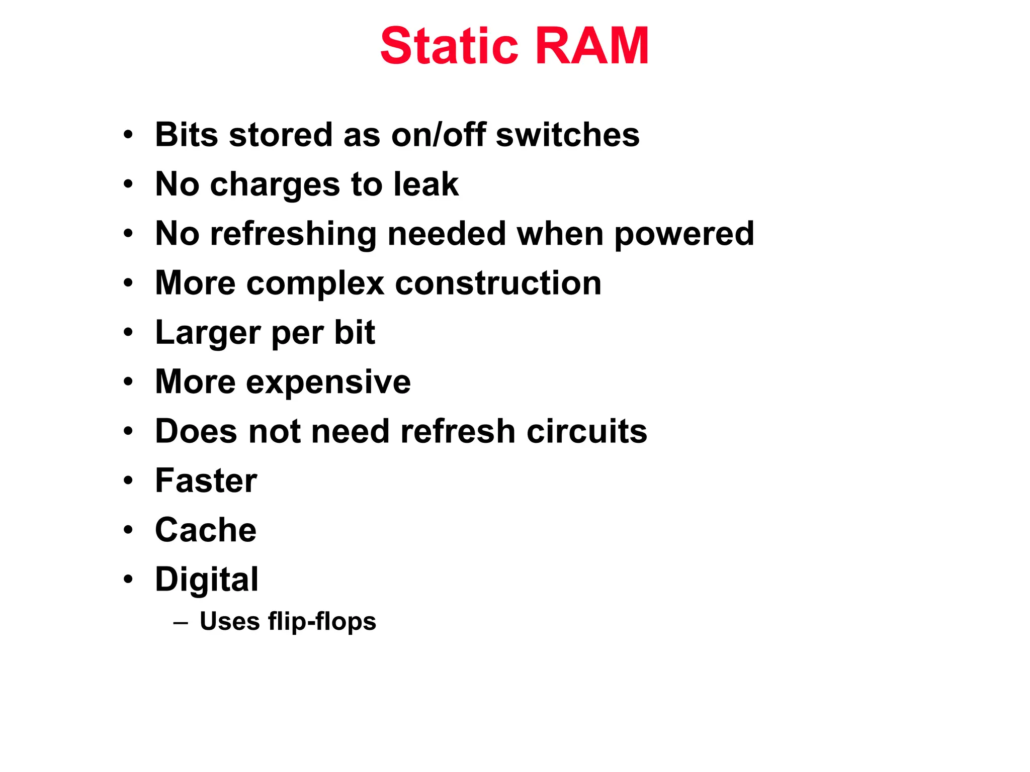
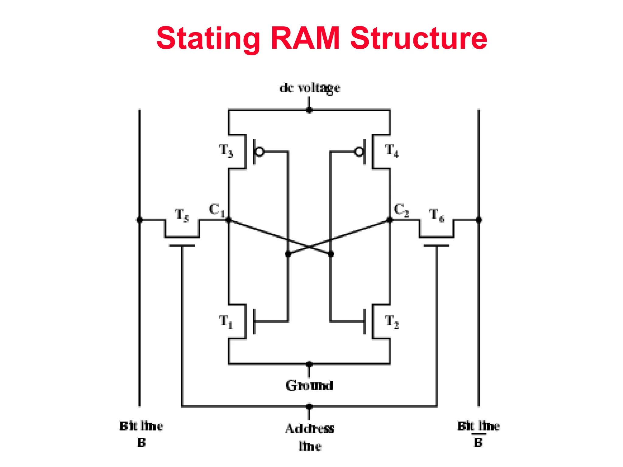
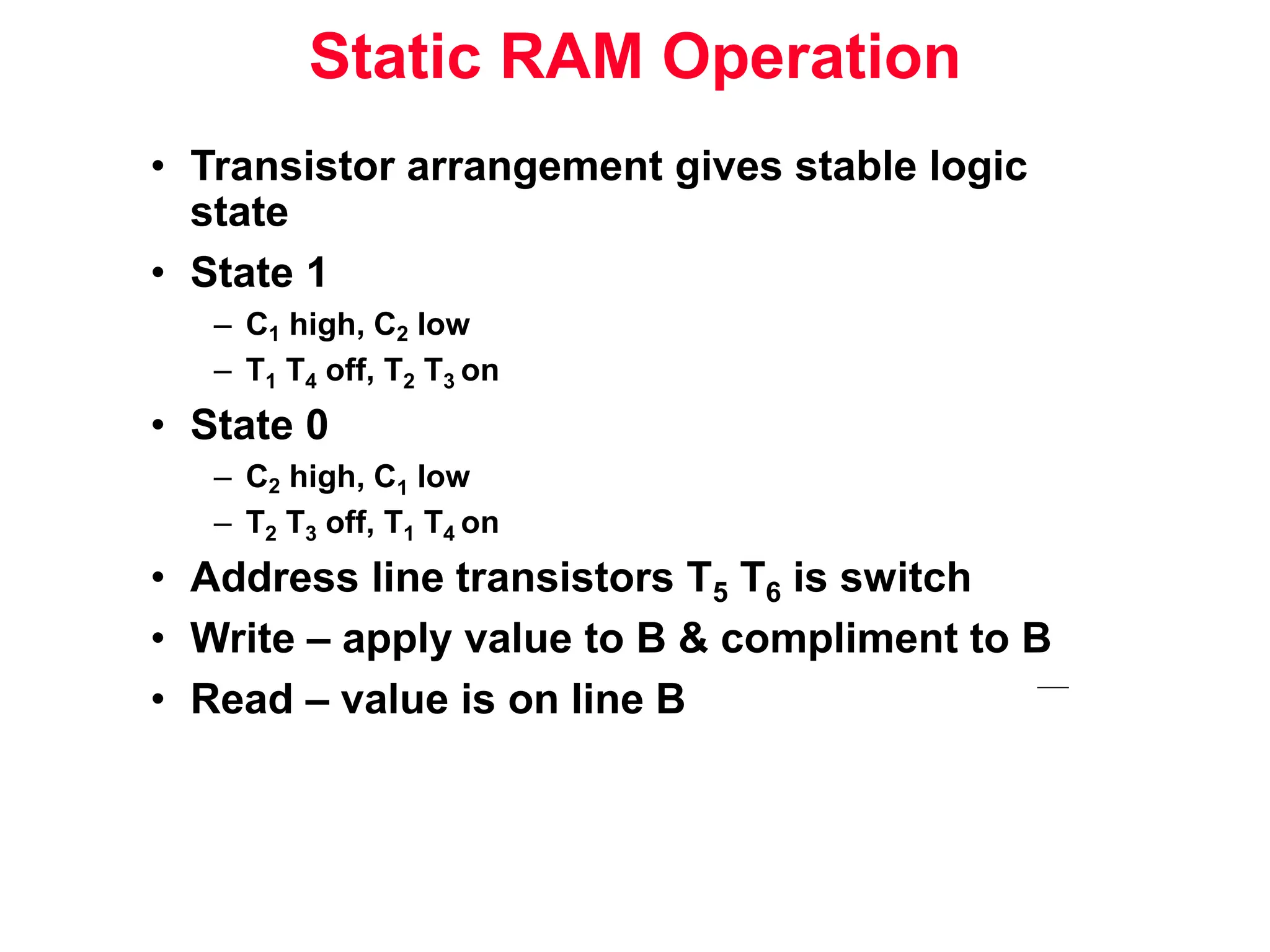
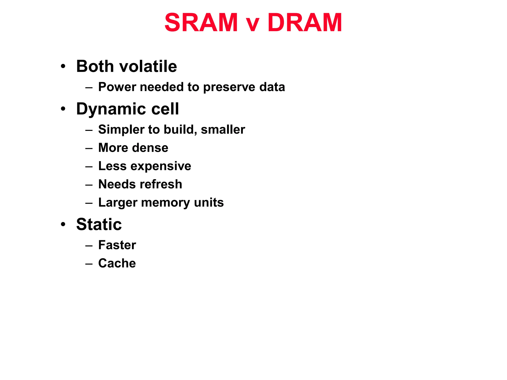
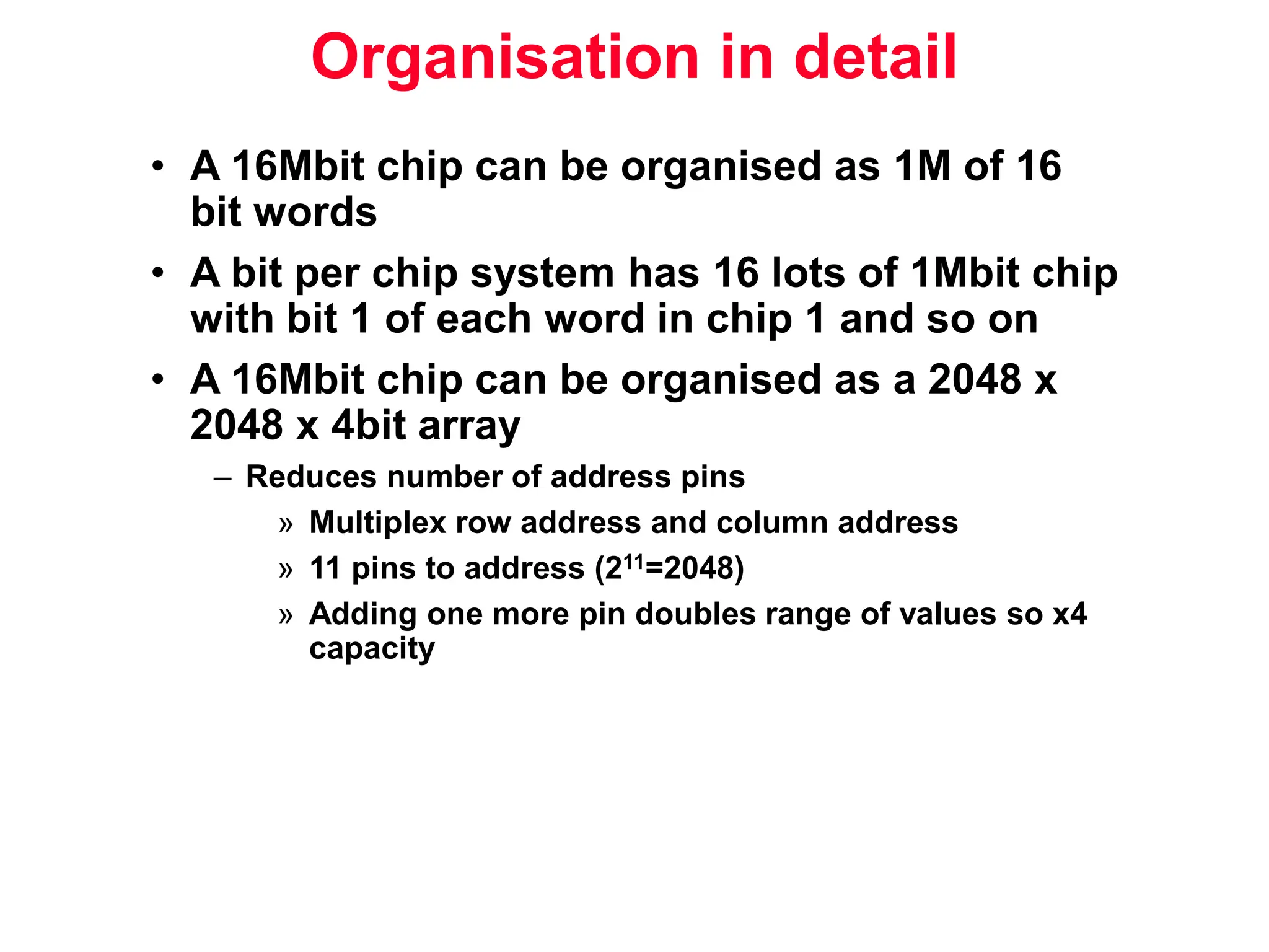
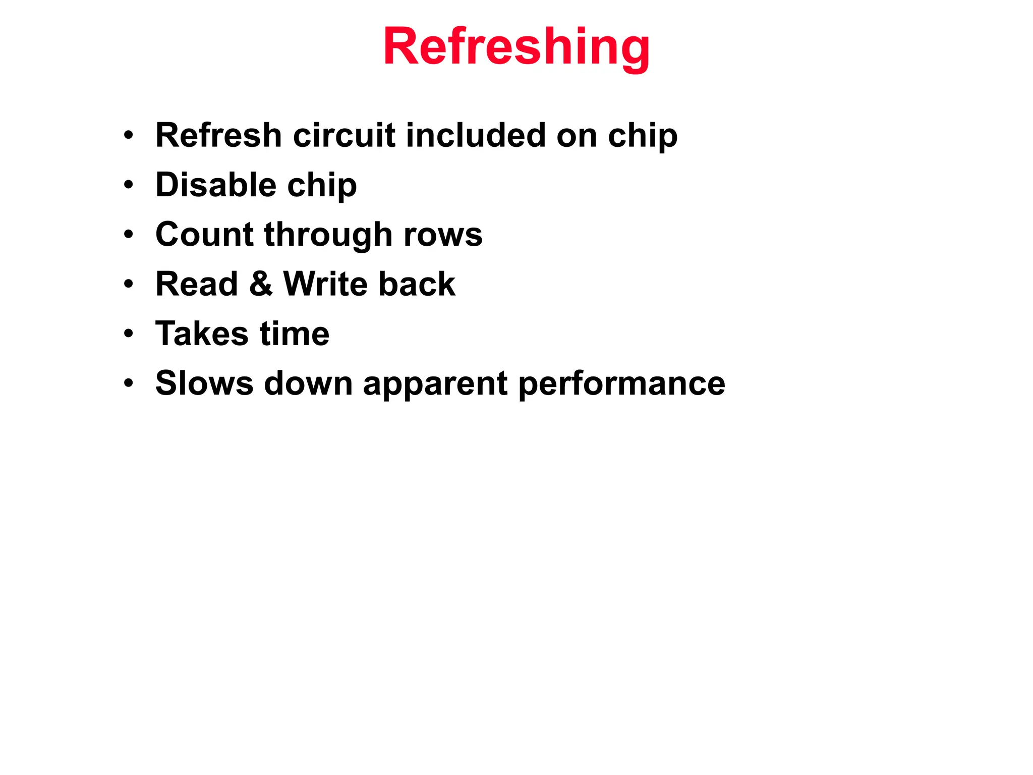
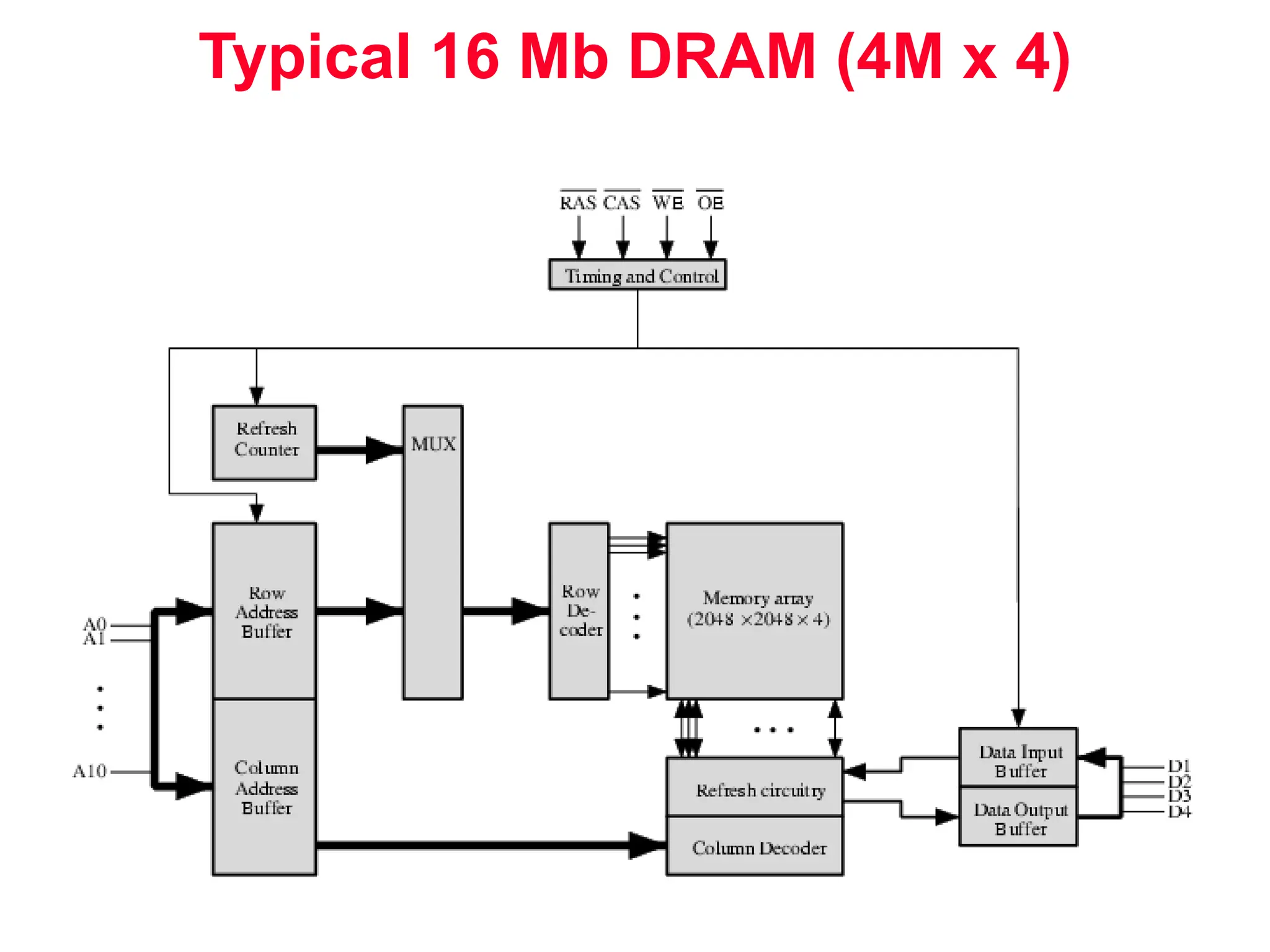
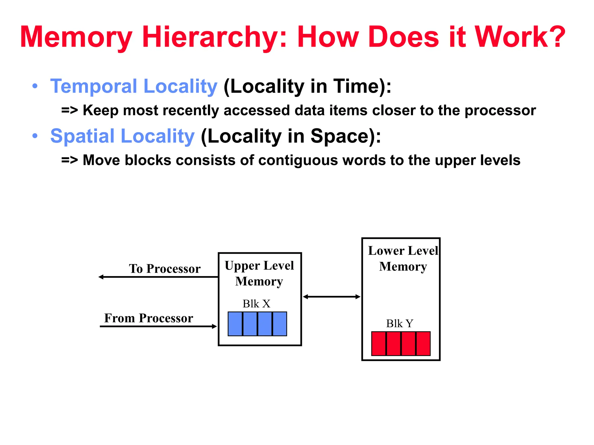
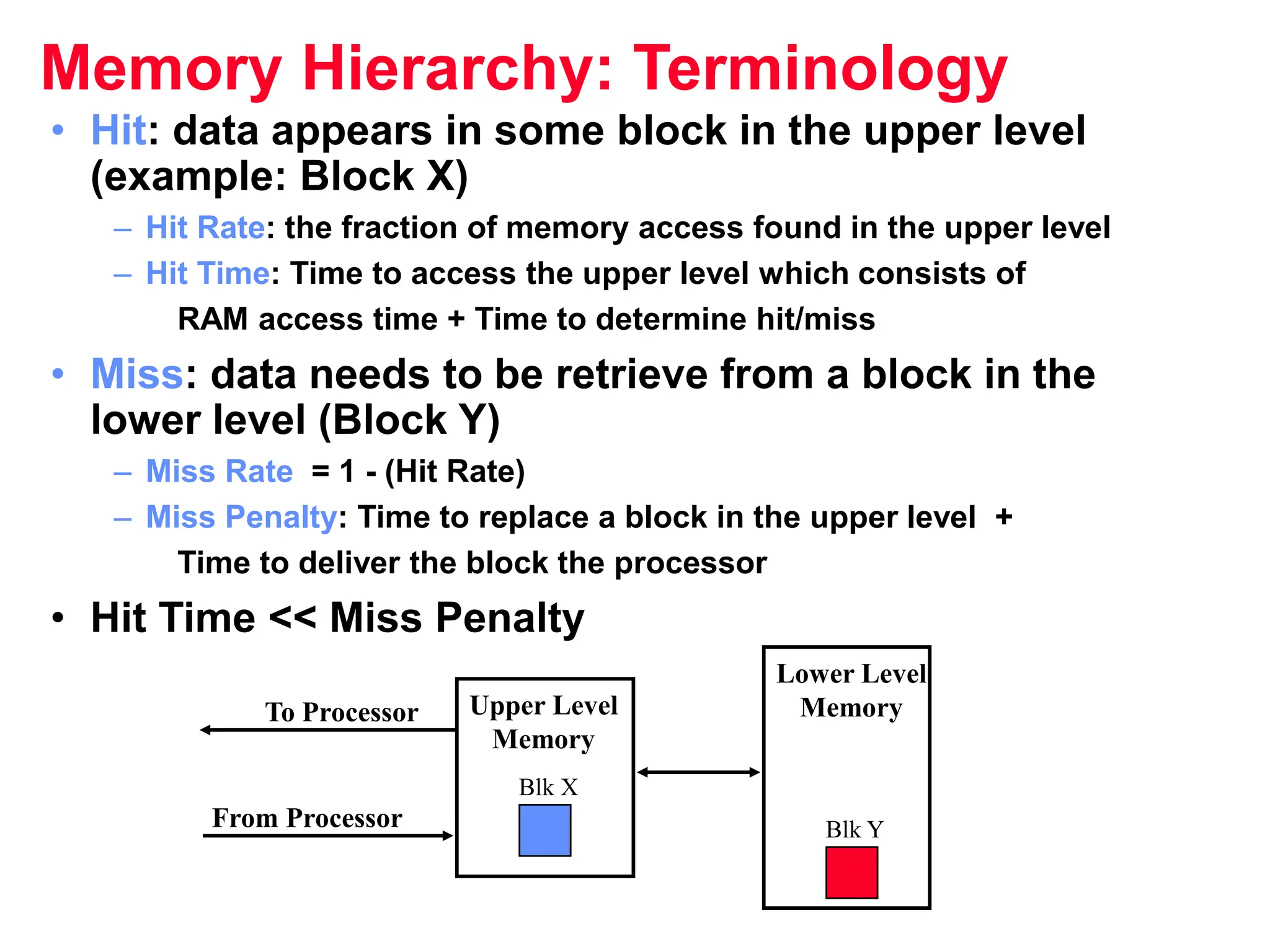
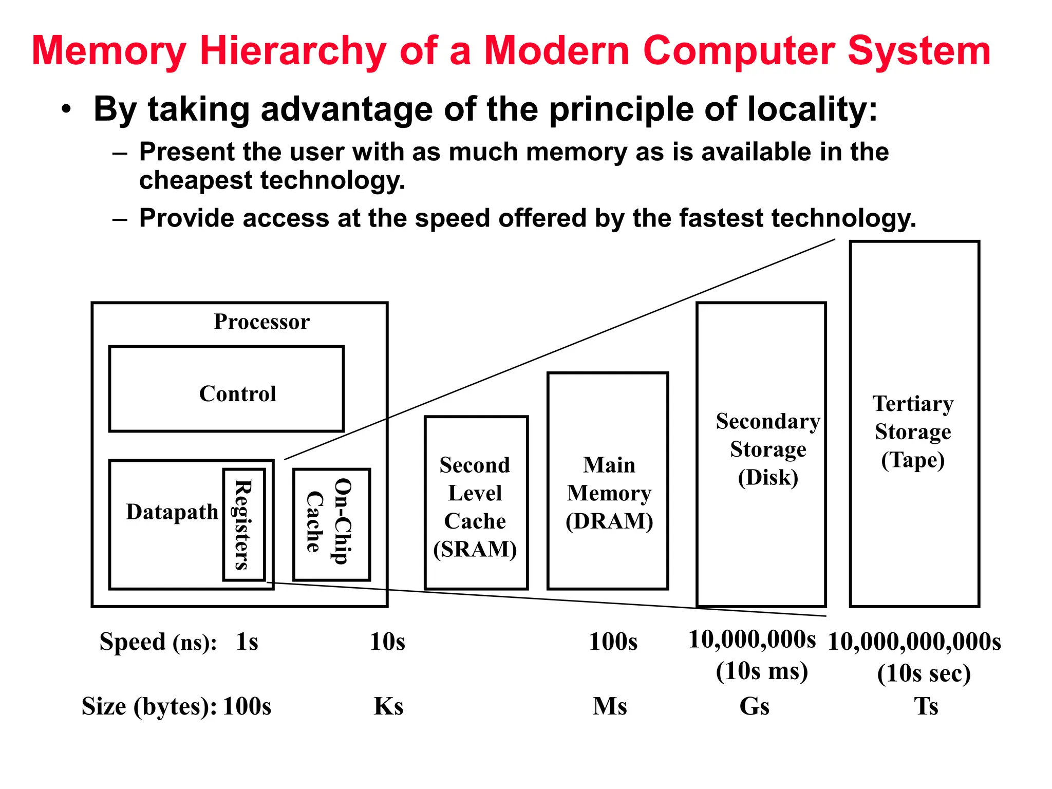
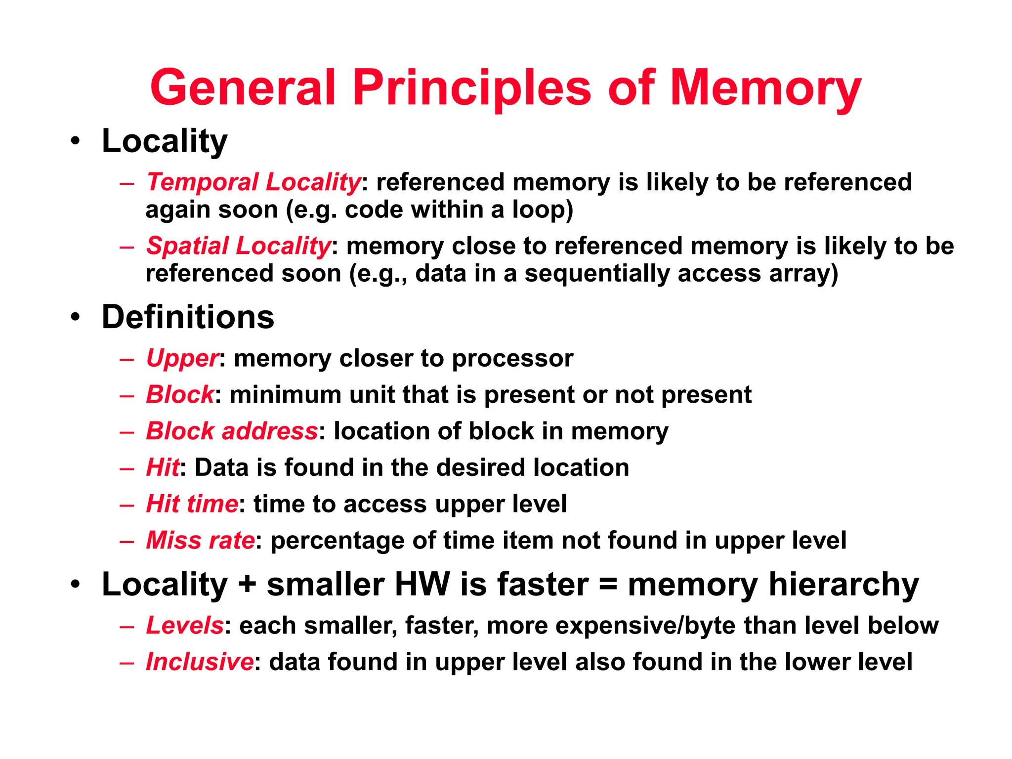
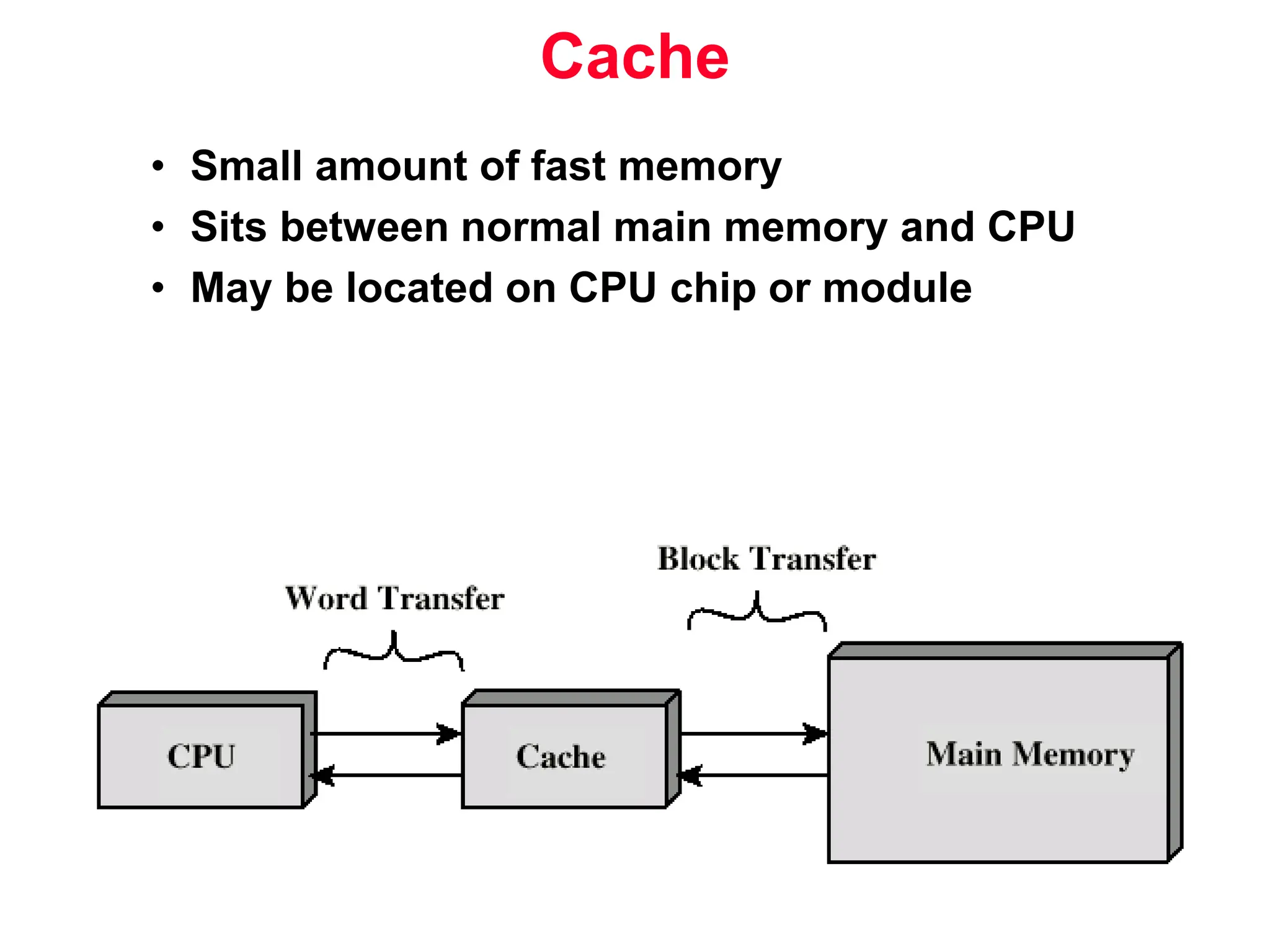
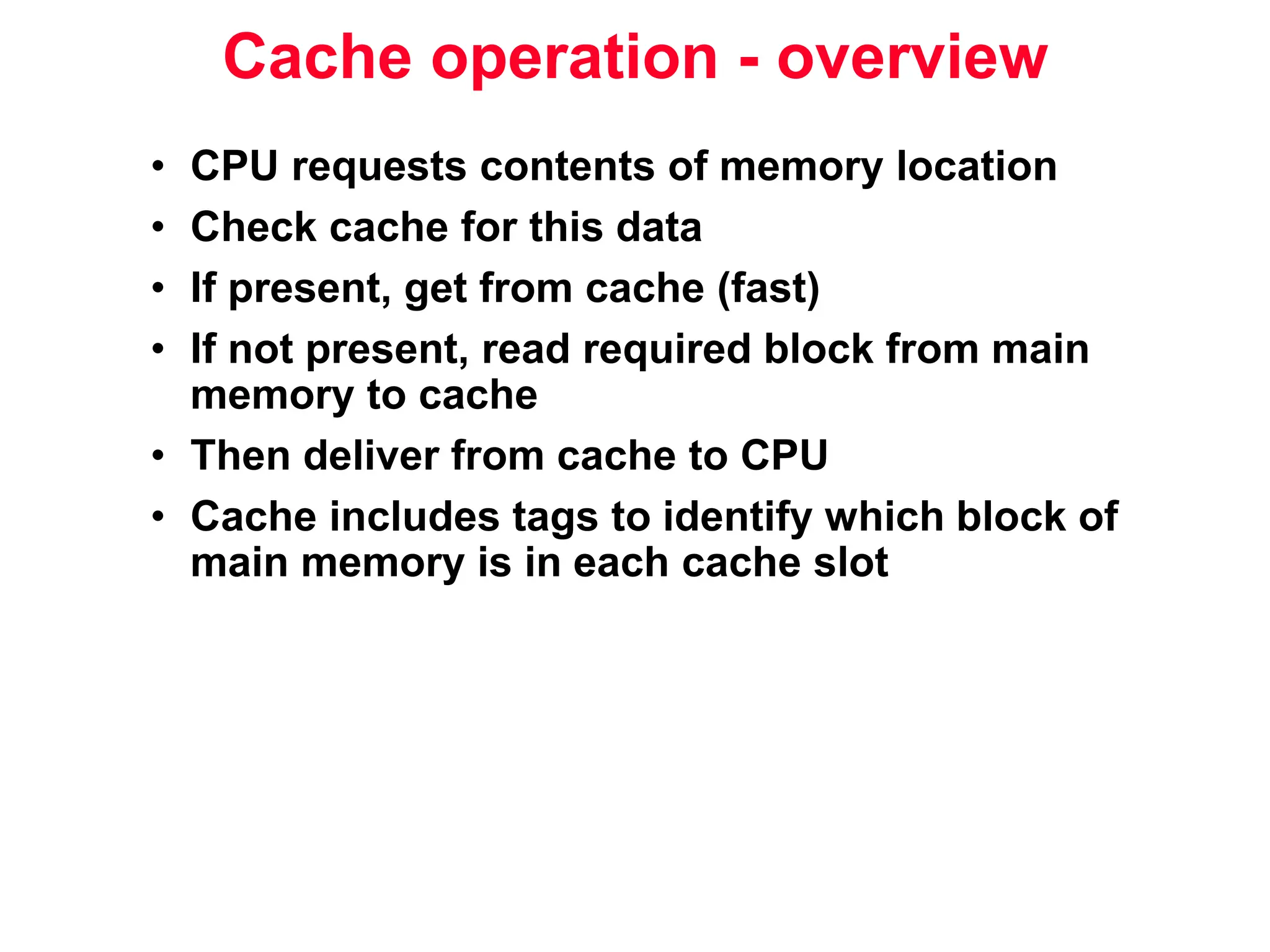
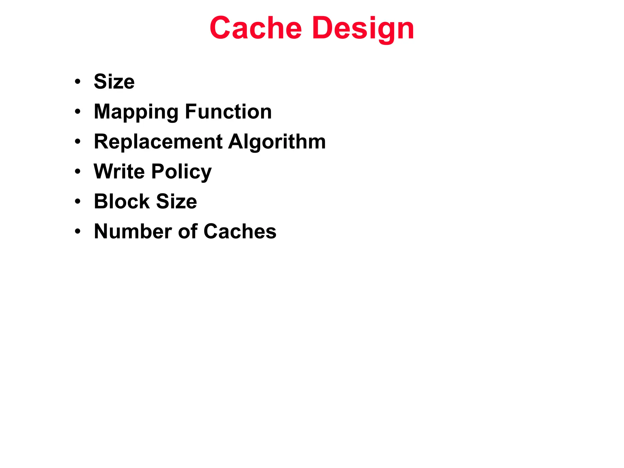
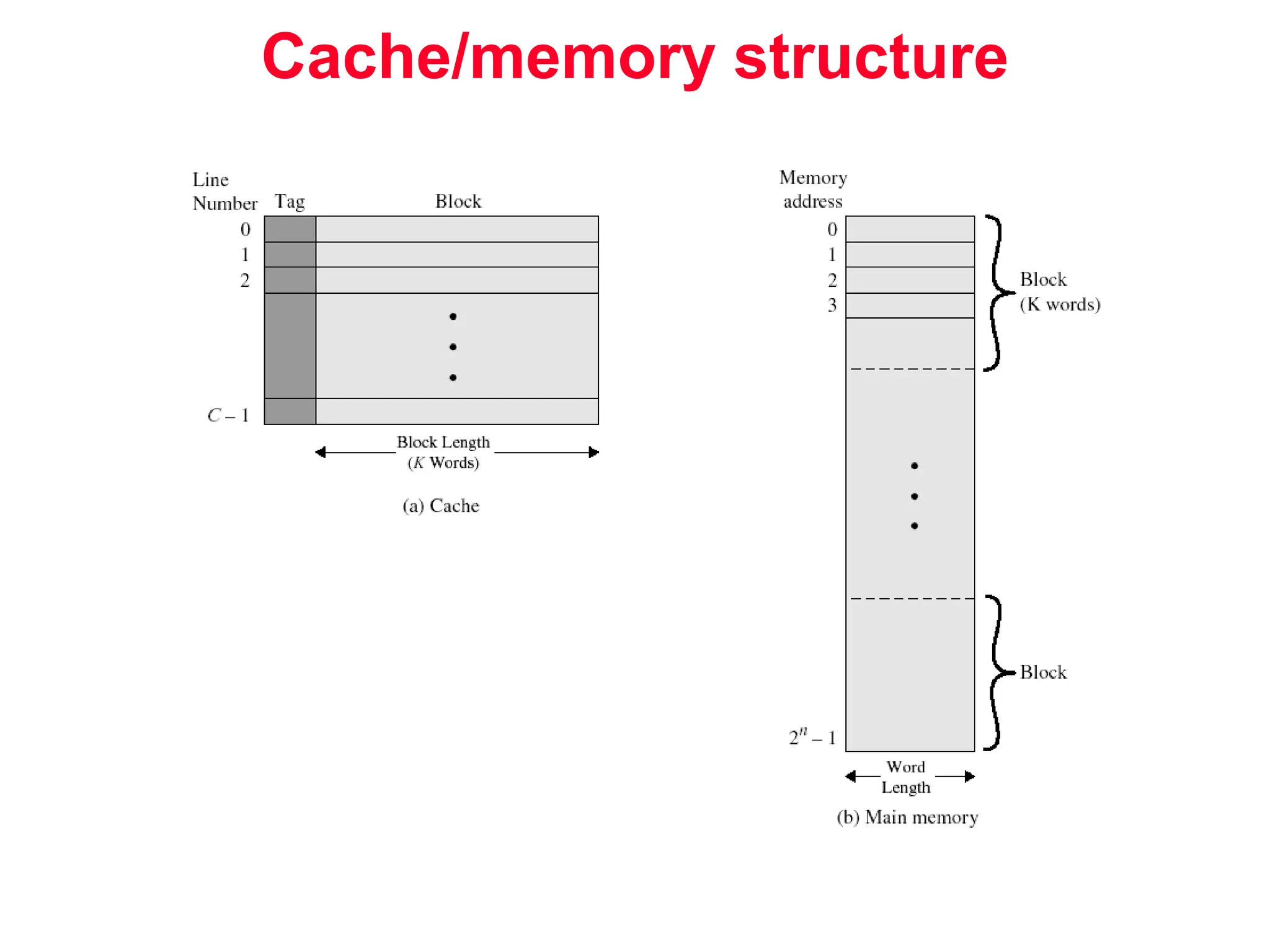
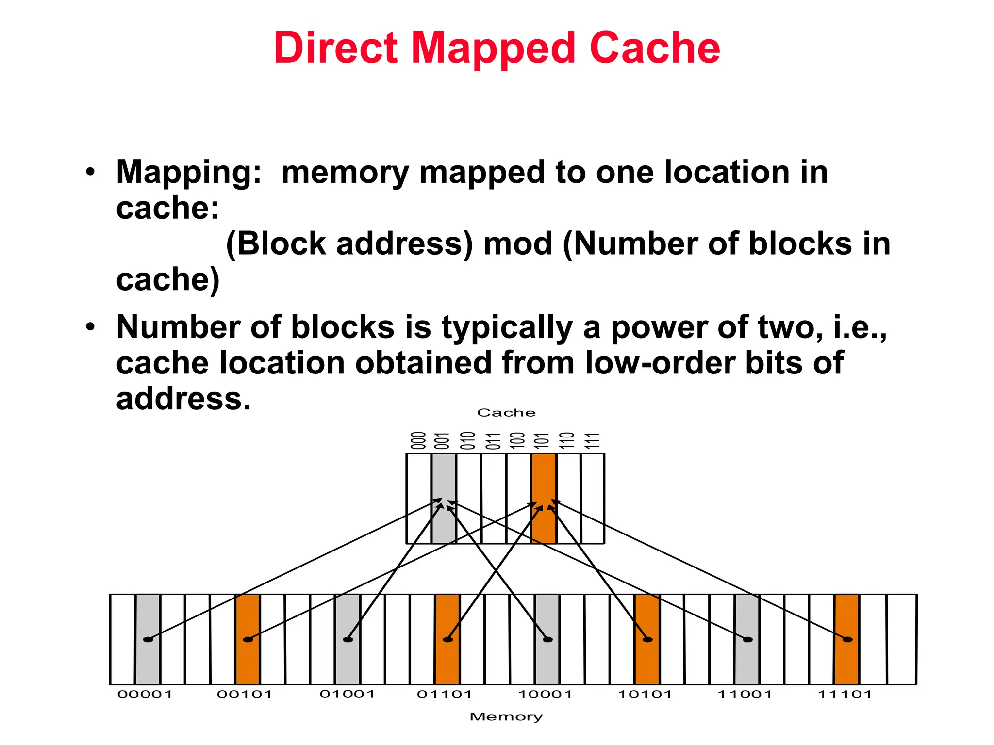
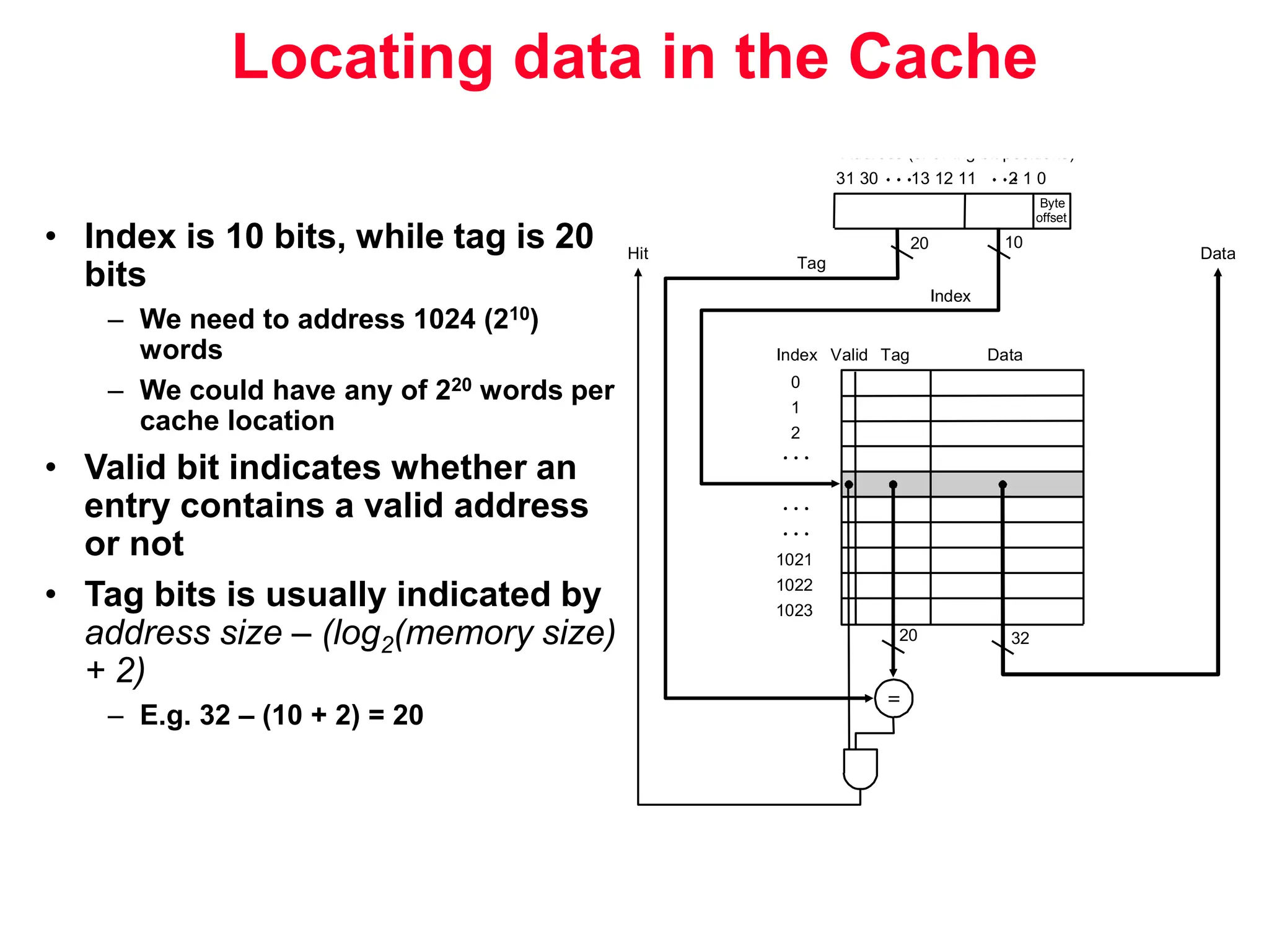
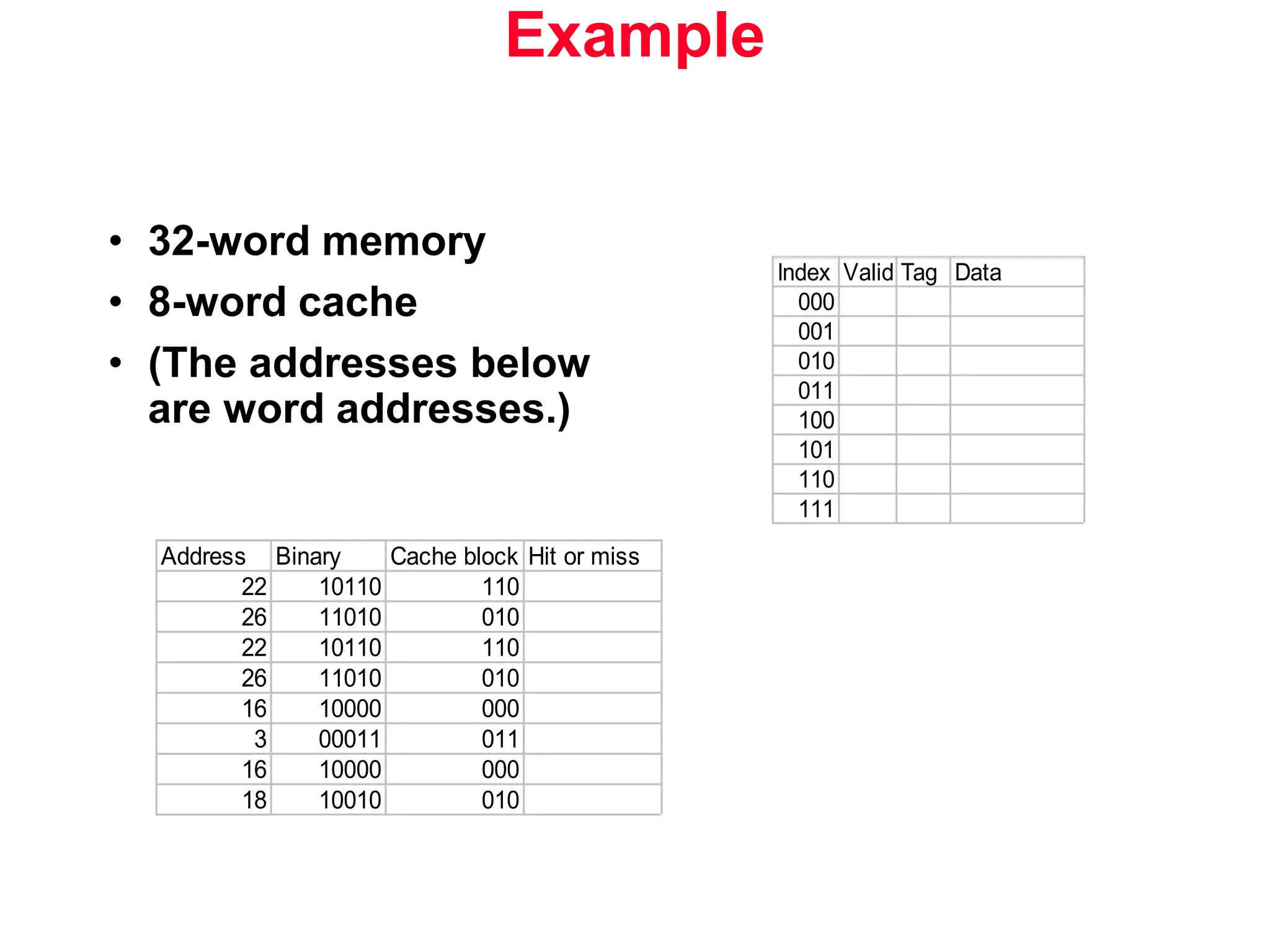
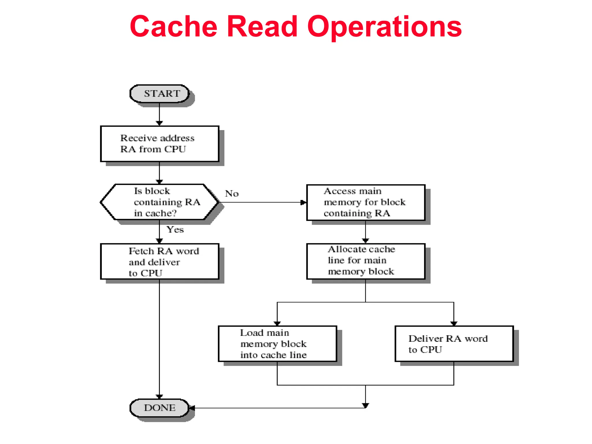
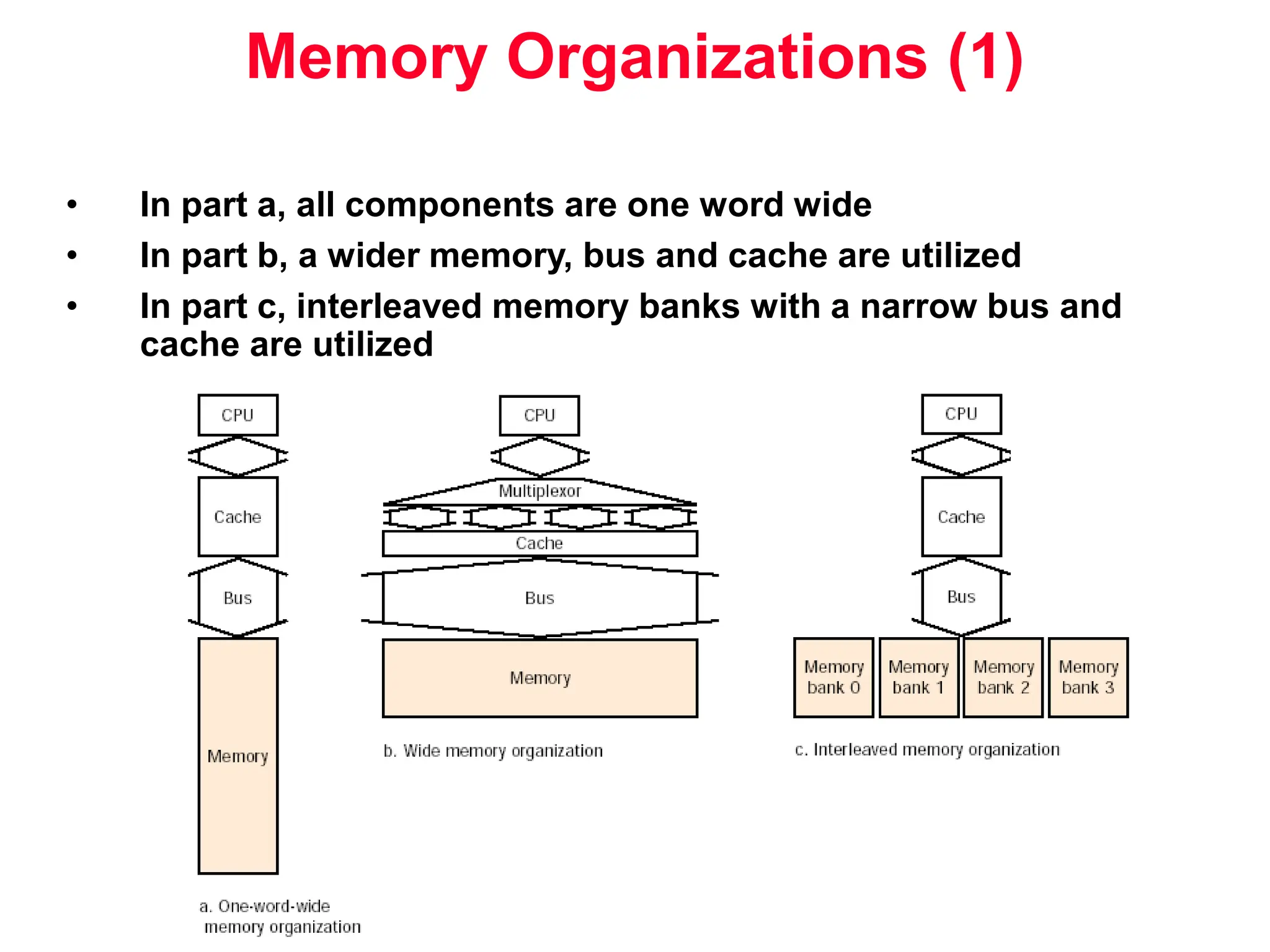
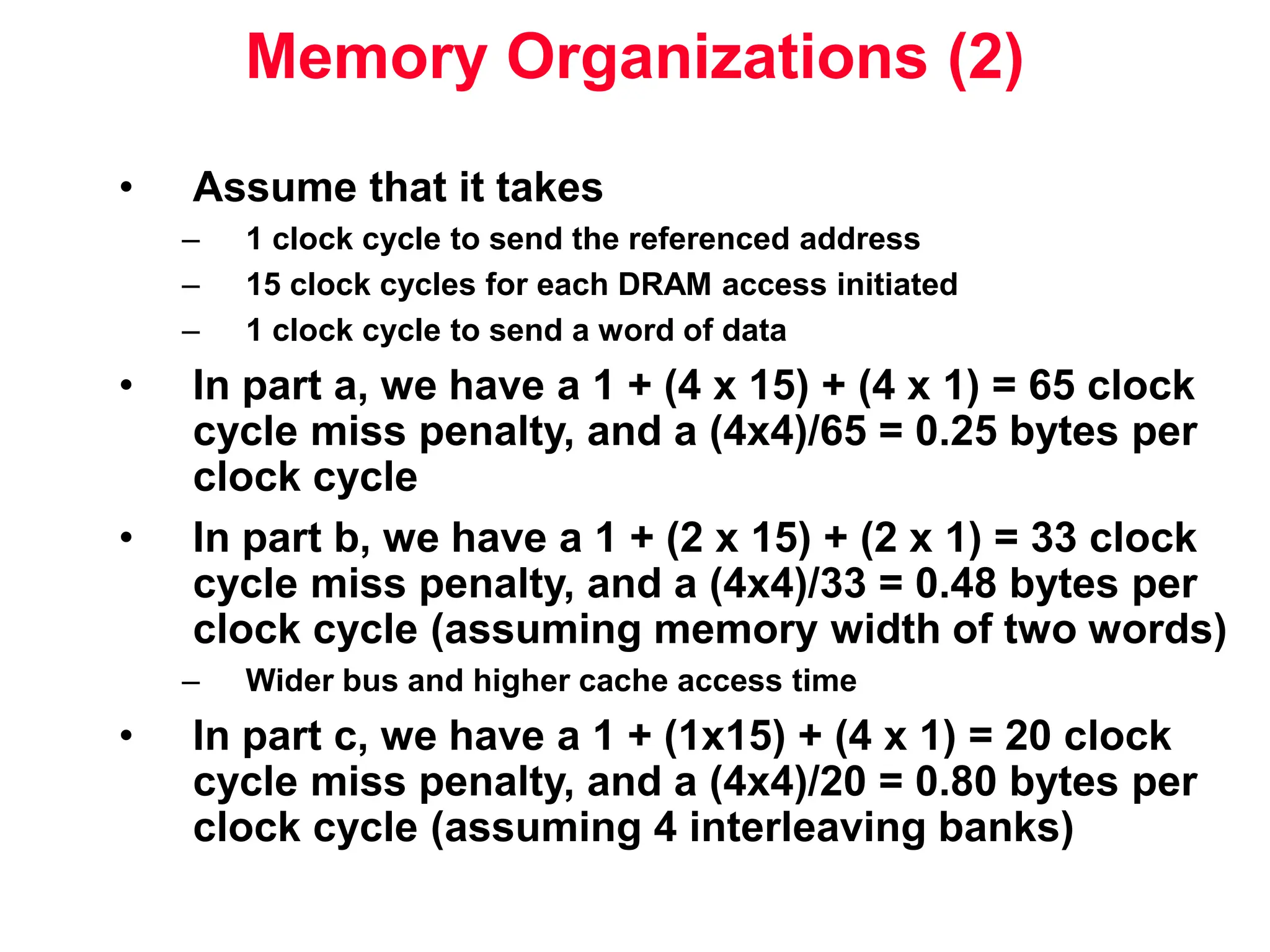
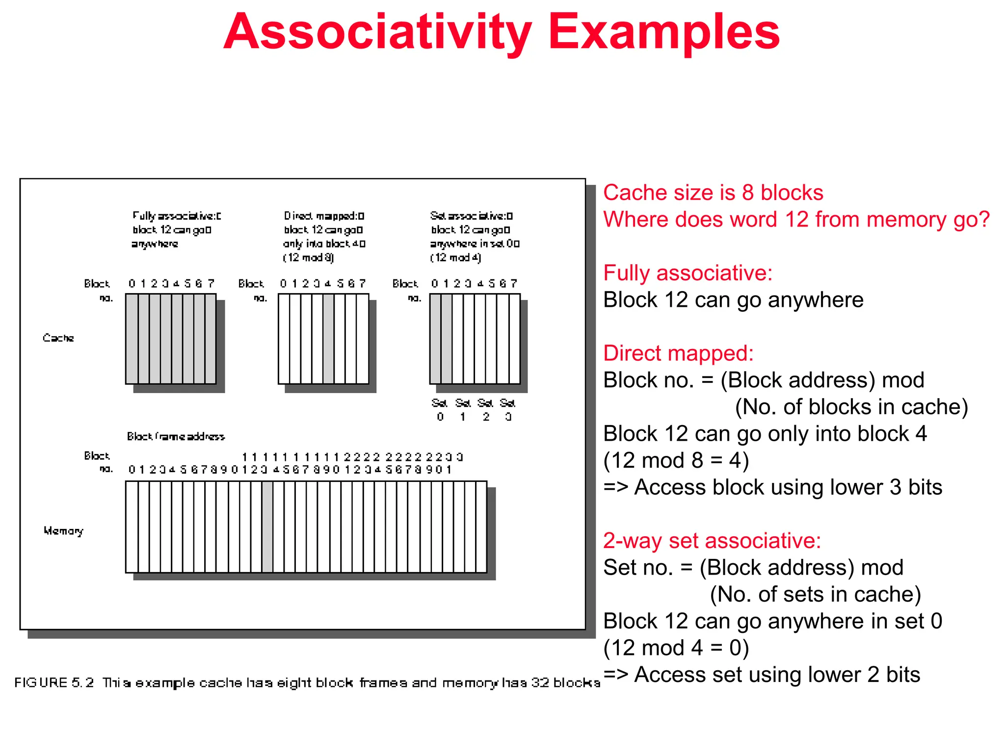
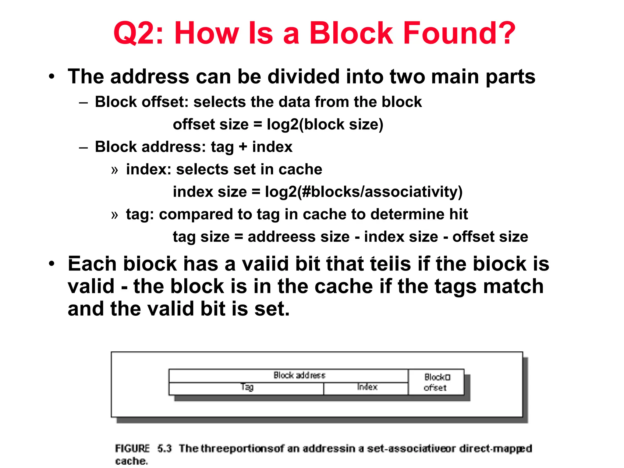
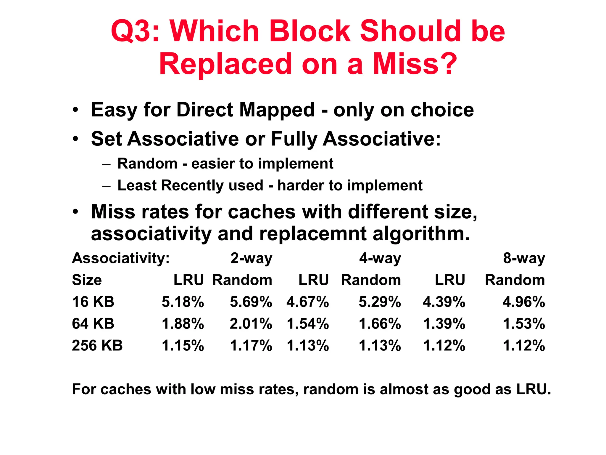
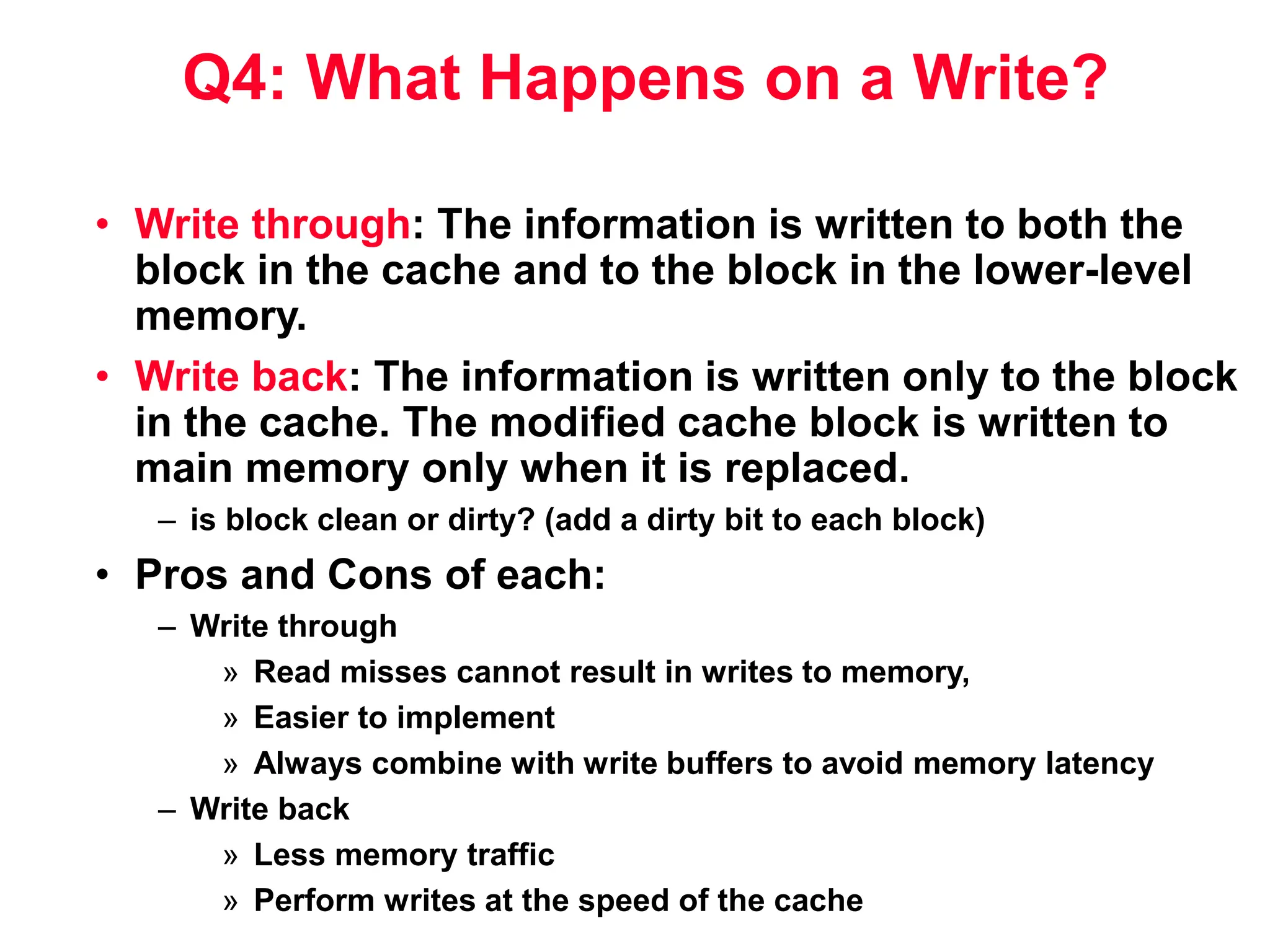
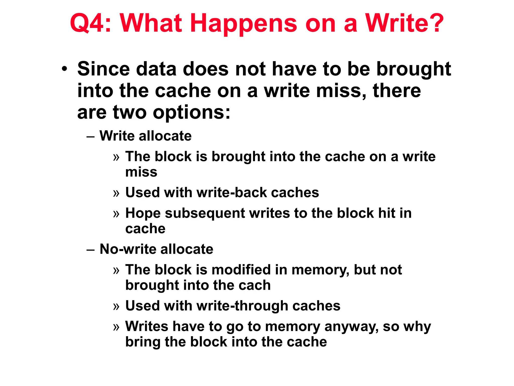
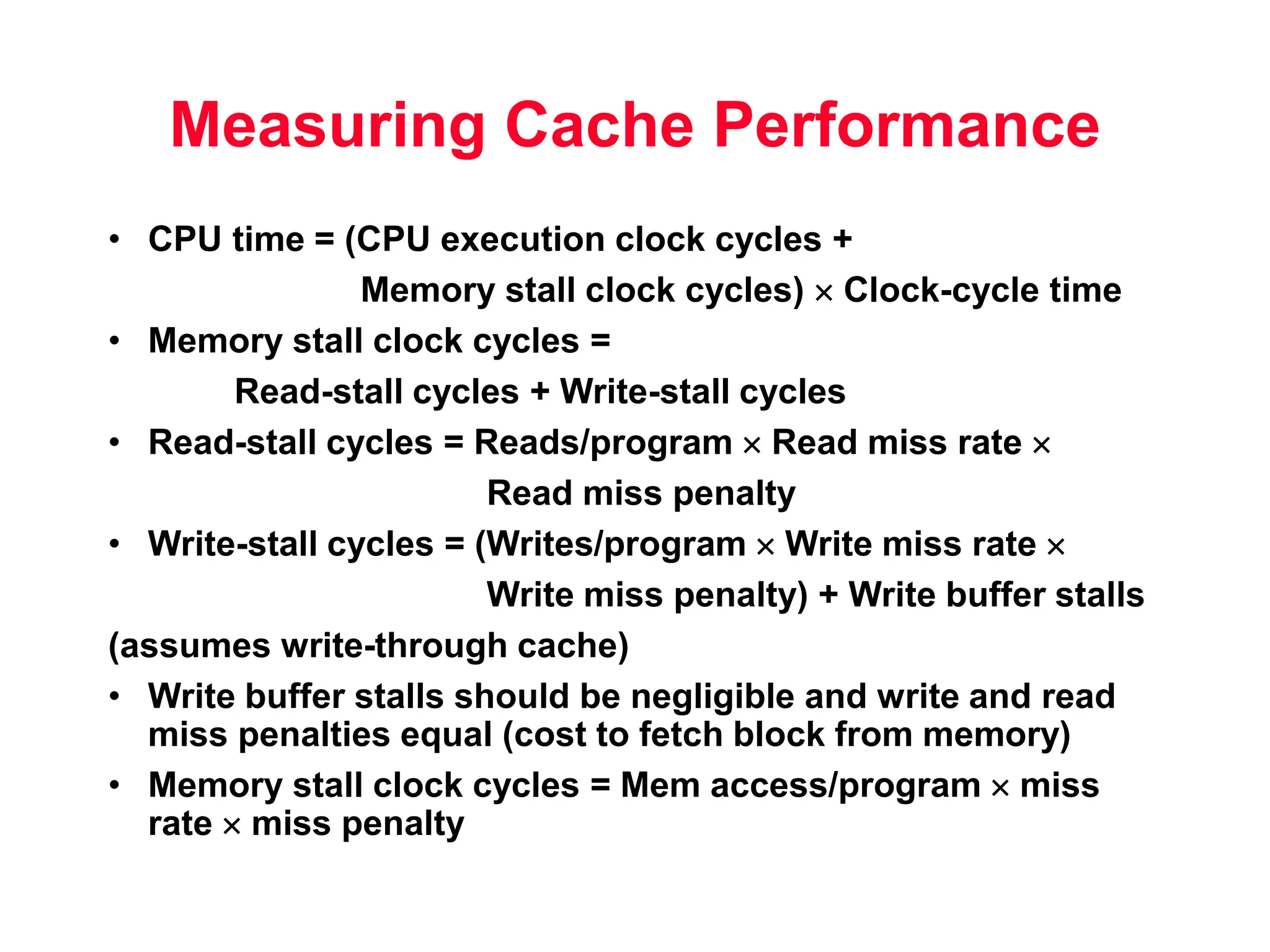
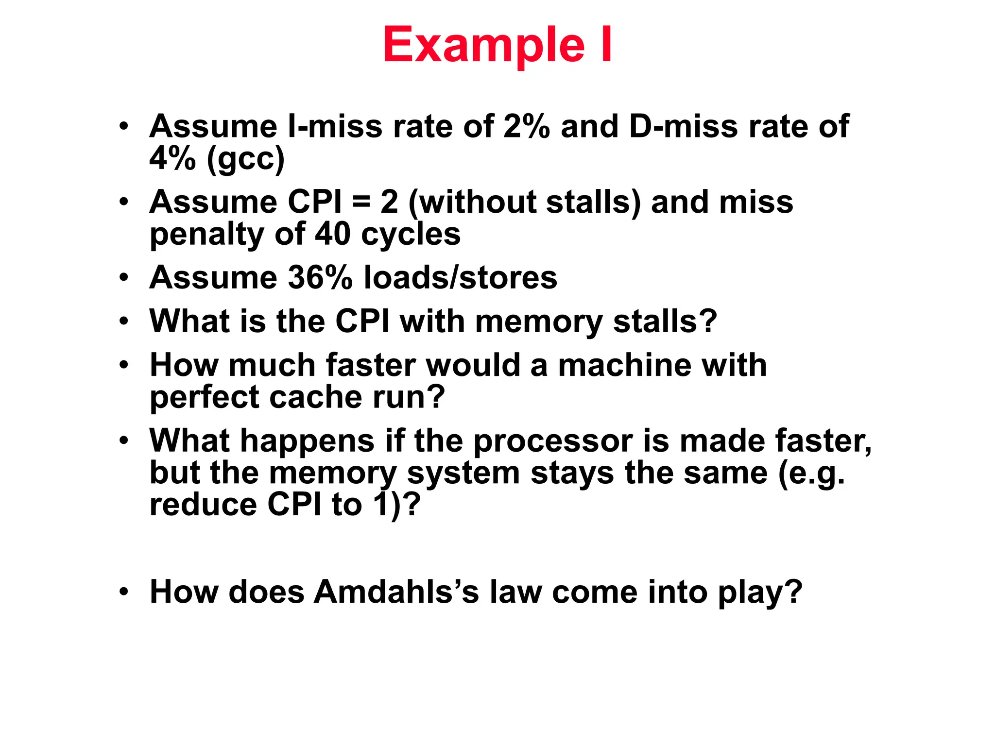
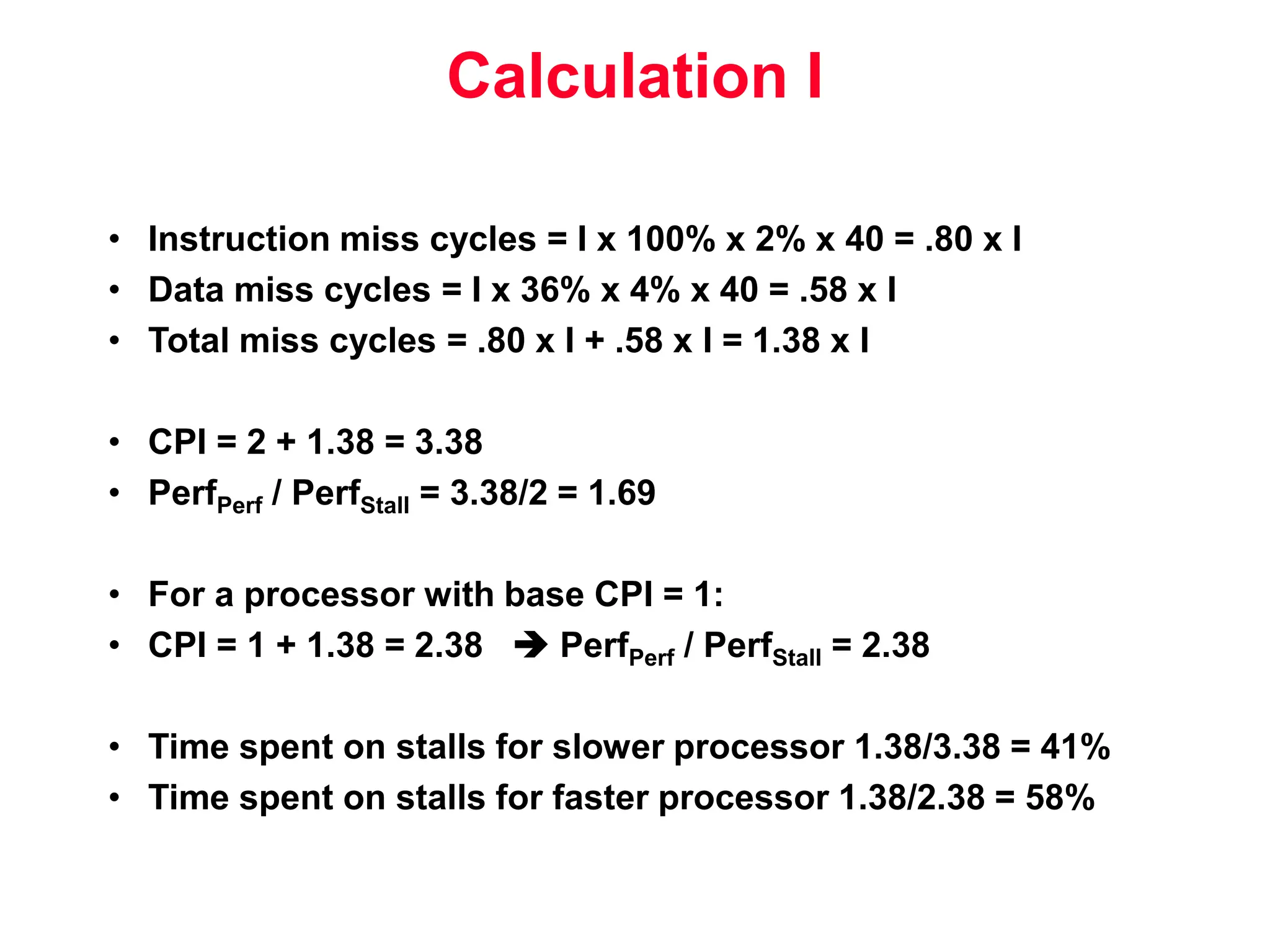
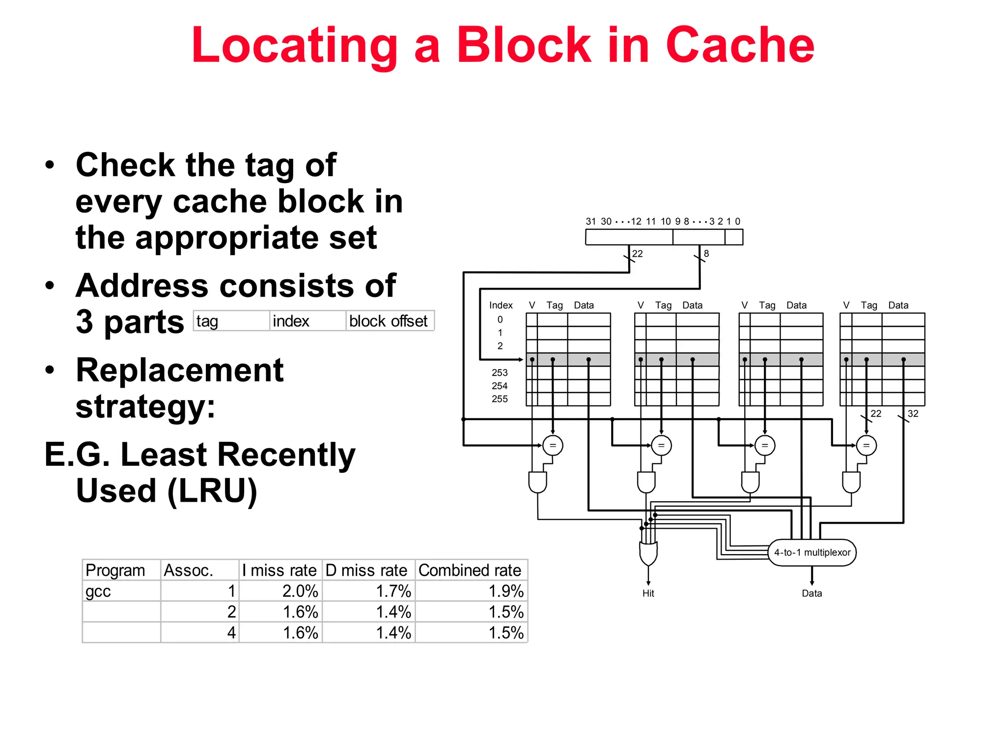
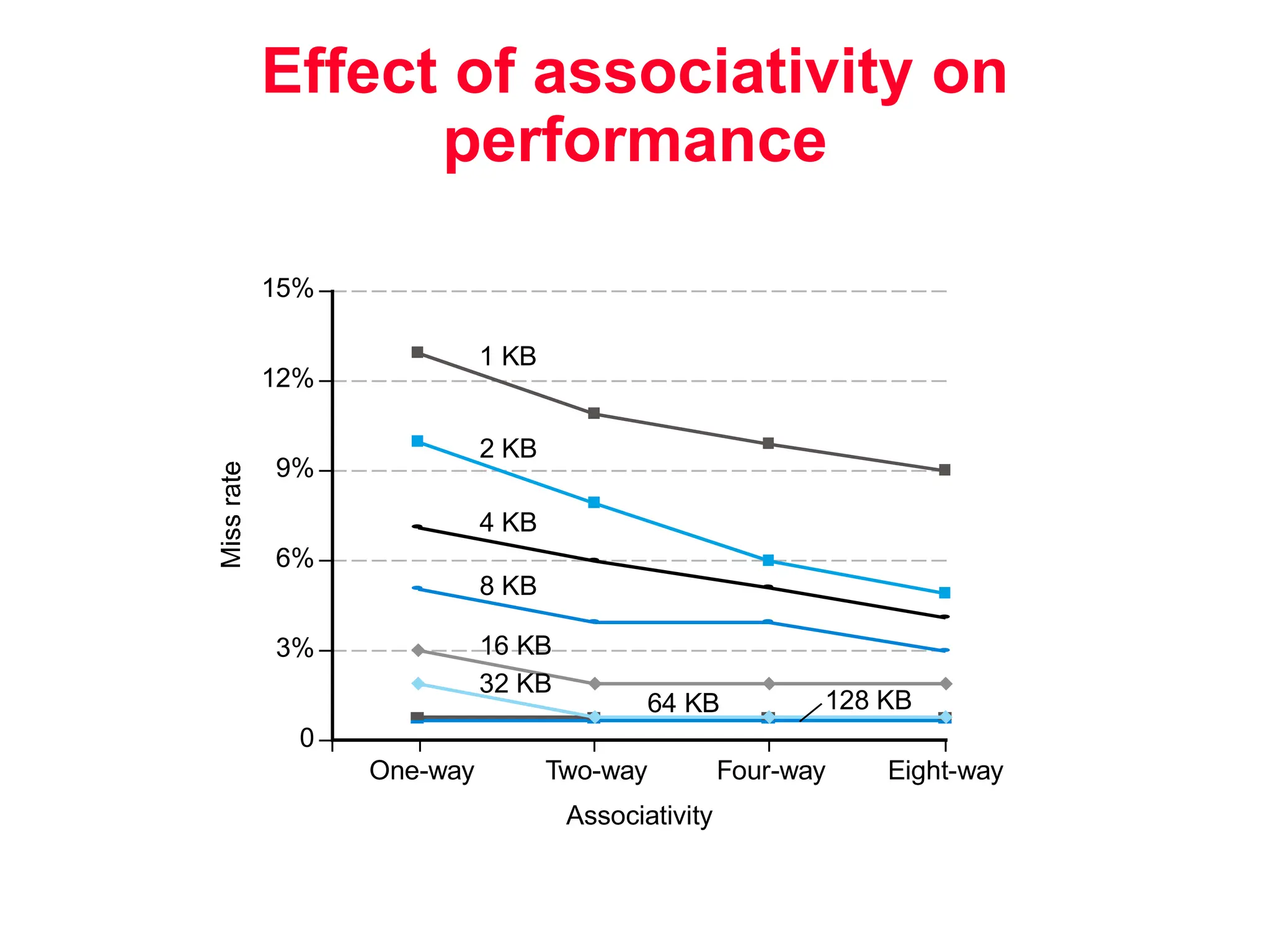
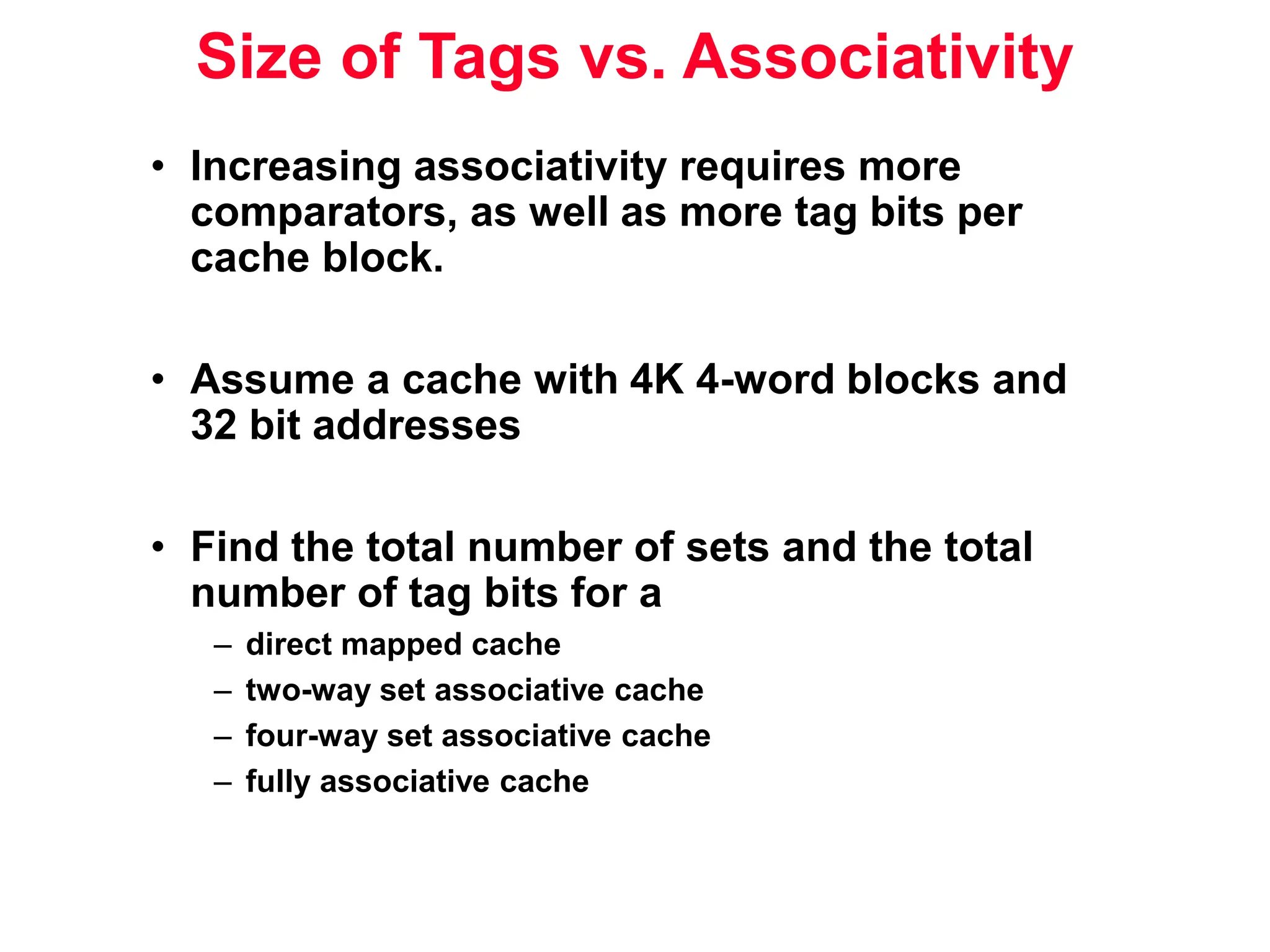
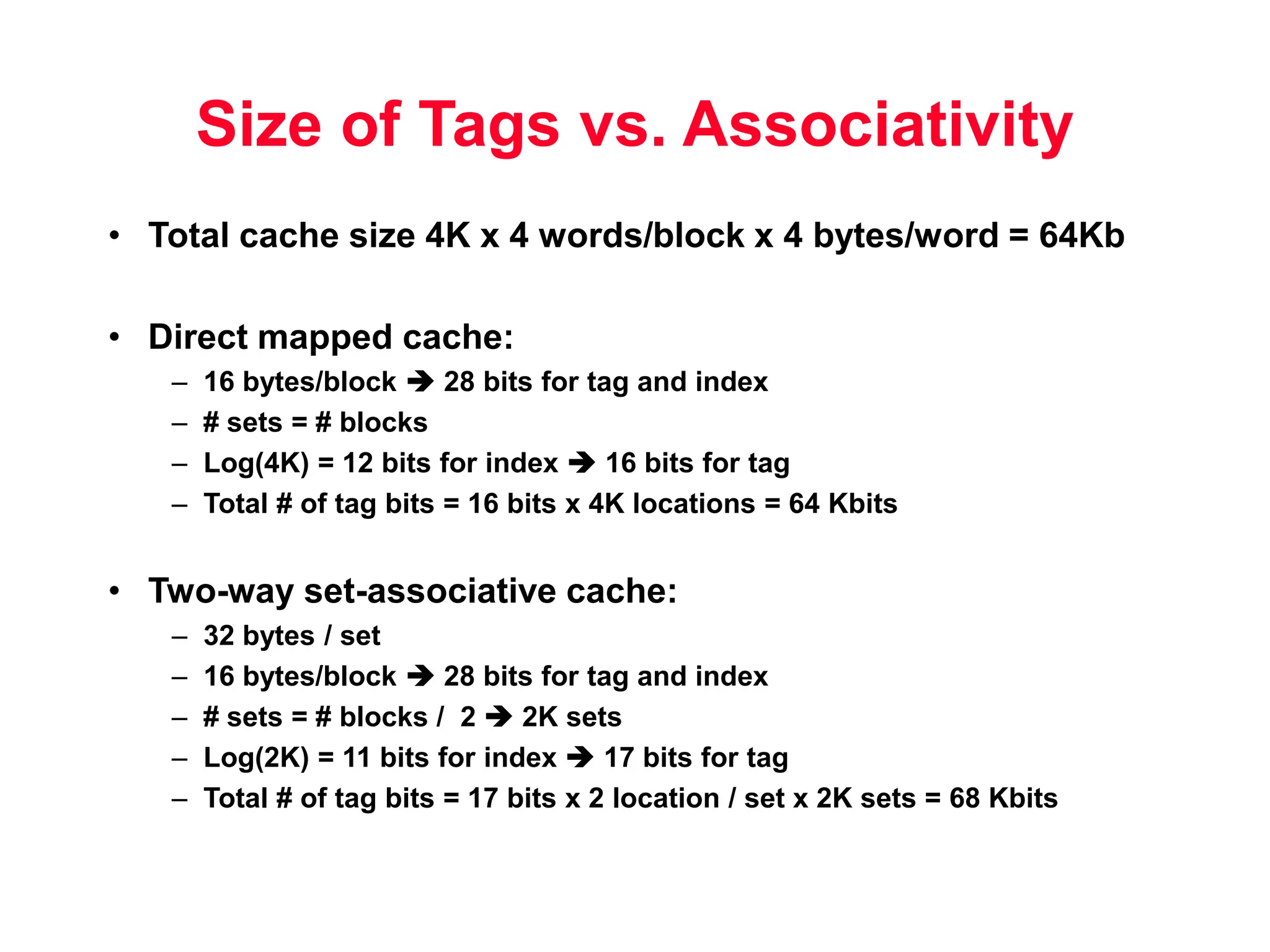
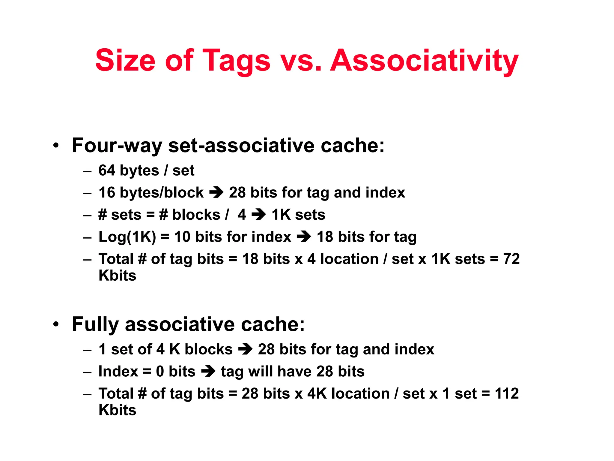
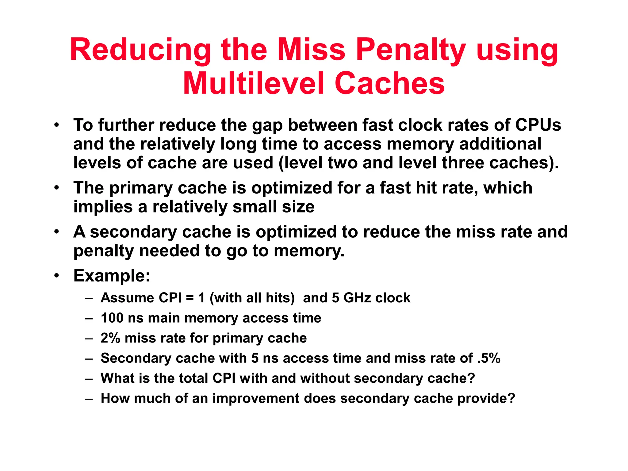
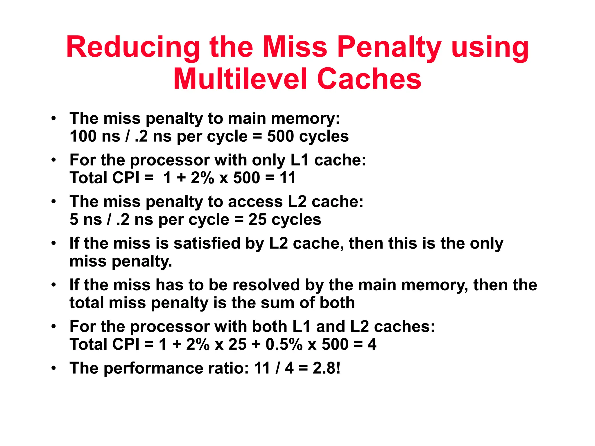
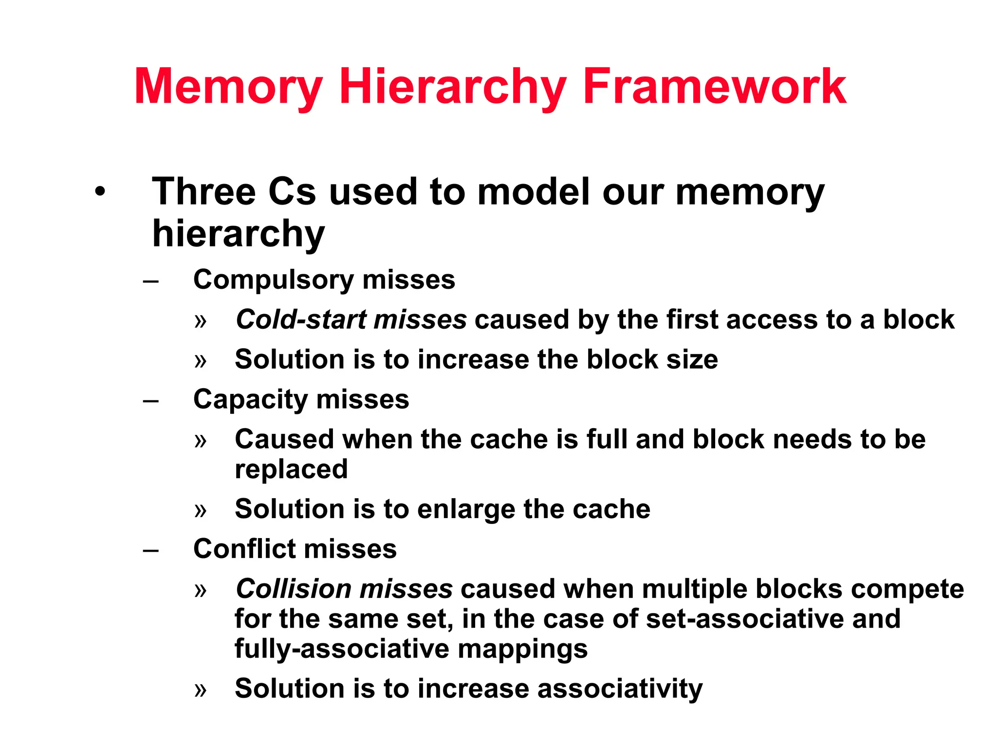
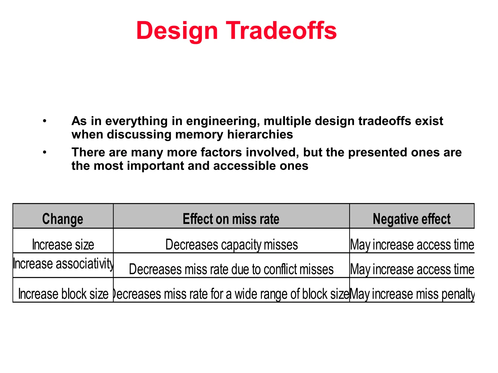
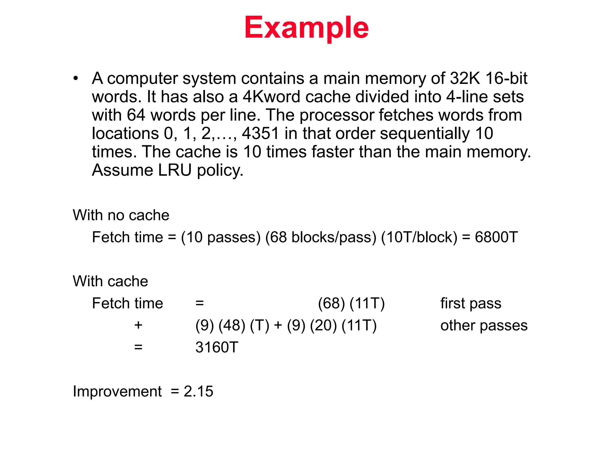
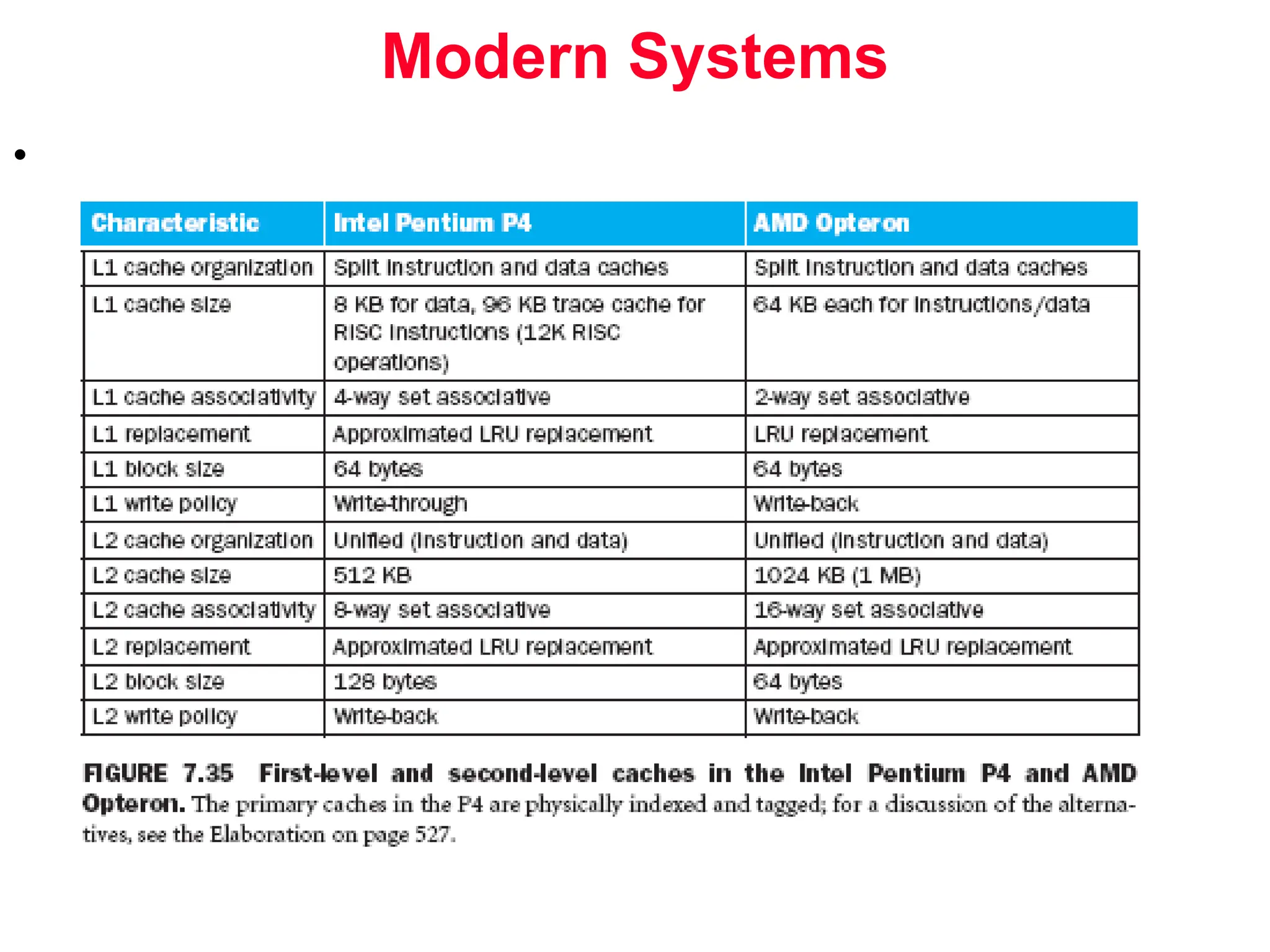
Memory Hierarchy and Cache Design The following sources are used for preparing these slides: • Lecture 14 from the course Computer architecture ECE 201 by Professor Mike Schulte. • Lecture 4 from William Stallings, Computer Organization and Architecture, Prentice Hall; 6th edition, July 15, 2002. • Lecture 6 from the course Systems Architectures II by Professors Jeremy R. Johnson and Anatole D. Ruslanov • Some of figures are from Computer Organization and Design: The Hardware/Software Approach, Third Edition, by David Patterson and John Hennessy, are copyrighted material (COPYRIGHT 2004 MORGAN KAUFMANN PUBLISHERS, INC. ALL RIGHTS RESERVED).
• The Five Classic Components of a Computer • Memory is usually implemented as: – Dynamic Random Access Memory (DRAM) - for main memory – Static Random Access Memory (SRAM) - for cache The Big Picture: Where are We Now? Control Datapath Memory Processor Input Output
Technology Trends (from 1st lecture) DRAM Year Size Cycle Time 1980 64 Kb 250 ns 1983 256 Kb 220 ns 1986 1 Mb 190 ns 1989 4 Mb 165 ns 1992 16 Mb 145 ns 1995 64 Mb 120 ns 1998 256 Mb 100 ns 2001 1 Gb 80 ns Capacity Speed (latency) Logic: 2x in 3 years 2x in 3 years DRAM: 4x in 3 years 2x in 10 years Disk: 4x in 3 years 2x in 10 years 1000:1! 2:1!
µProc 60%/yr. (2X/1.5yr) DRAM 9%/yr. (2X/10 yrs) 1 10 100 1000 1980 1981 1983 1984 1985 1986 1987 1988 1989 1990 1991 1992 1993 1994 1995 1996 1997 1998 1999 2000 DRAM CPU 1982 Processor-Memory Performance Gap: (grows 50% / year) Performance Time “Moore’s Law” Processor-DRAM Memory Gap (latency) Who Cares About Memory?
Memory Hierarchy CPU Level n Level 2 Level 1 Levels in the memory hierarchy Increasing distance from the CPU in access time Size of the memory at each level Processor Data are transferred Memory technology Typical access time $ per GB in 2004 SRAM 0.5–5 ns $4000–$10,000 DRAM 50–70 ns $100–$200 Magnetic disk 5,000,000–20,000,000 ns $0.50–$2
• SRAM: – Value is stored on a pair of inverting gates – Very fast but takes up more space than DRAM (4 to 6 transistors) • DRAM: – Value is stored as a charge on capacitor (must be refreshed) – Very small but slower than SRAM (factor of 5 to 10) Memory
Memory Cell Operation
Dynamic RAM • Bits stored as charge in capacitors • Charges leak • Need refreshing even when powered • Simpler construction • Smaller per bit • Less expensive • Need refresh circuits • Slower • Main memory • Essentially analogue – Level of charge determines value
Dynamic RAM Structure
DRAM Operation • Address line active when bit read or written – Transistor switch closed (current flows) • Write – Voltage to bit line » High for 1 low for 0 – Then signal address line » Transfers charge to capacitor • Read – Address line selected » transistor turns on – Charge from capacitor fed via bit line to sense amplifier » Compares with reference value to determine 0 or 1 – Capacitor charge must be restored
Static RAM • Bits stored as on/off switches • No charges to leak • No refreshing needed when powered • More complex construction • Larger per bit • More expensive • Does not need refresh circuits • Faster • Cache • Digital – Uses flip-flops
Stating RAM Structure
Static RAM Operation • Transistor arrangement gives stable logic state • State 1 – C1 high, C2 low – T1 T4 off, T2 T3 on • State 0 – C2 high, C1 low – T2 T3 off, T1 T4 on • Address line transistors T5 T6 is switch • Write – apply value to B & compliment to B • Read – value is on line B
SRAM v DRAM • Both volatile – Power needed to preserve data • Dynamic cell – Simpler to build, smaller – More dense – Less expensive – Needs refresh – Larger memory units • Static – Faster – Cache
Organisation in detail • A 16Mbit chip can be organised as 1M of 16 bit words • A bit per chip system has 16 lots of 1Mbit chip with bit 1 of each word in chip 1 and so on • A 16Mbit chip can be organised as a 2048 x 2048 x 4bit array – Reduces number of address pins » Multiplex row address and column address » 11 pins to address (211=2048) » Adding one more pin doubles range of values so x4 capacity
Refreshing • Refresh circuit included on chip • Disable chip • Count through rows • Read & Write back • Takes time • Slows down apparent performance
Typical 16 Mb DRAM (4M x 4)
Memory Hierarchy: How Does it Work? • Temporal Locality (Locality in Time): => Keep most recently accessed data items closer to the processor • Spatial Locality (Locality in Space): => Move blocks consists of contiguous words to the upper levels Lower Level Memory Upper Level Memory To Processor From Processor Blk X Blk Y
Memory Hierarchy: Terminology • Hit: data appears in some block in the upper level (example: Block X) – Hit Rate: the fraction of memory access found in the upper level – Hit Time: Time to access the upper level which consists of RAM access time + Time to determine hit/miss • Miss: data needs to be retrieve from a block in the lower level (Block Y) – Miss Rate = 1 - (Hit Rate) – Miss Penalty: Time to replace a block in the upper level + Time to deliver the block the processor • Hit Time << Miss Penalty Lower Level Memory Upper Level Memory To Processor From Processor Blk X Blk Y
Memory Hierarchy of a Modern Computer System • By taking advantage of the principle of locality: – Present the user with as much memory as is available in the cheapest technology. – Provide access at the speed offered by the fastest technology. Control Datapath Secondary Storage (Disk) Processor Registers Main Memory (DRAM) Second Level Cache (SRAM) On-Chip Cache 1s 10,000,000s (10s ms) Speed (ns): 10s 100s 100s Gs Size (bytes): Ks Ms Tertiary Storage (Tape) 10,000,000,000s (10s sec) Ts
General Principles of Memory • Locality – Temporal Locality: referenced memory is likely to be referenced again soon (e.g. code within a loop) – Spatial Locality: memory close to referenced memory is likely to be referenced soon (e.g., data in a sequentially access array) • Definitions – Upper: memory closer to processor – Block: minimum unit that is present or not present – Block address: location of block in memory – Hit: Data is found in the desired location – Hit time: time to access upper level – Miss rate: percentage of time item not found in upper level • Locality + smaller HW is faster = memory hierarchy – Levels: each smaller, faster, more expensive/byte than level below – Inclusive: data found in upper level also found in the lower level
Cache • Small amount of fast memory • Sits between normal main memory and CPU • May be located on CPU chip or module
Cache operation - overview • CPU requests contents of memory location • Check cache for this data • If present, get from cache (fast) • If not present, read required block from main memory to cache • Then deliver from cache to CPU • Cache includes tags to identify which block of main memory is in each cache slot
Cache Design • Size • Mapping Function • Replacement Algorithm • Write Policy • Block Size • Number of Caches
Relationship of Caches and Pipeline WB Data Adder IF/ID ALU Memory Reg File MUX Data Memory MUX Sign Extend Zero? MEM/WB EX/MEM 4 Adder Next SEQ PC RD RD RD Next PC Address RS1 RS2 Imm MUX ID/EX I-$ D-$ Memory
Cache/memory structure
• Mapping: memory mapped to one location in cache: (Block address) mod (Number of blocks in cache) • Number of blocks is typically a power of two, i.e., cache location obtained from low-order bits of address. Direct Mapped Cache 00001 00101 01001 01101 10001 10101 11001 11101 000 Cache Memory 001 010 011 100 101 110 111
Locating data in the Cache • Index is 10 bits, while tag is 20 bits – We need to address 1024 (210) words – We could have any of 220 words per cache location • Valid bit indicates whether an entry contains a valid address or not • Tag bits is usually indicated by address size – (log2(memory size) + 2) – E.g. 32 – (10 + 2) = 20 Address (showing bit positions) 20 10 Byte offset Valid Tag Data Index 0 1 2 1021 1022 1023 Tag Index Hit Data 20 32 31 30 13 12 11 2 1 0
Example • 32-word memory • 8-word cache • (The addresses below are word addresses.) Address Binary Cache block Hit or miss 22 10110 110 26 11010 010 22 10110 110 26 11010 010 16 10000 000 3 00011 011 16 10000 000 18 10010 010 Index Valid Tag Data 000 001 010 011 100 101 110 111
Example-Bits in Cache • How many total bits are required for a direct- mapping cache with 16KB of data and 4-word blocks, assuming a 32-bit address.
Example – Mapping an Address to a Cache Block • Consider a cache with 64 blocks and a block size of 16 bytes. What block number does byte address 1200 (10010110000b) map to? What’s about 1204?
Cache Misses - Read • The control unit 1. must detect a miss 2. Stall the entire processor 3. fetch the requested data from memory • Steps taken by the control unit on an instruction cache miss 1. Send PC-4 to memory 2. Start reading the main memory 3. Transferring block to the cache 4. Restart the instruction to start fetching from the cache
Cache Read Operations
Cache Misses - Writes • On an instruction cache miss, we – Index the cache using bits 15-2 of the address – Write the cache entry » Data from processor is placed in data portion » Bits 31-16 of address written into tag field » Turn valid bit on – Write the word to main memory using the entire address • How do we keep main memory up to date ? – Write-through means writing to both cache and main memory when a miss occurs (to avoid inconsistent or untrue memories) – Write buffer uses a fast and small memory to store the cache writes while it is waiting to be written out to memory (in MIPS, it is 4 words) – Write-back means writing out to main memory only when the block is swapped out
Memory Organizations (1) • In part a, all components are one word wide • In part b, a wider memory, bus and cache are utilized • In part c, interleaved memory banks with a narrow bus and cache are utilized
Memory Organizations (2) • Assume that it takes – 1 clock cycle to send the referenced address – 15 clock cycles for each DRAM access initiated – 1 clock cycle to send a word of data • In part a, we have a 1 + (4 x 15) + (4 x 1) = 65 clock cycle miss penalty, and a (4x4)/65 = 0.25 bytes per clock cycle • In part b, we have a 1 + (2 x 15) + (2 x 1) = 33 clock cycle miss penalty, and a (4x4)/33 = 0.48 bytes per clock cycle (assuming memory width of two words) – Wider bus and higher cache access time • In part c, we have a 1 + (1x15) + (4 x 1) = 20 clock cycle miss penalty, and a (4x4)/20 = 0.80 bytes per clock cycle (assuming 4 interleaving banks)
Four Questions for Memory Hierarchy Designers • Q1: Where can a block be placed in the upper level? (Block placement) • Q2: How is a block found if it is in the upper level? (Block identification) • Q3: Which block should be replaced on a miss? (Block replacement) • Q4: What happens on a write? (Write strategy)
Q1: Where can a block be placed? • Direct Mapped: Each block has only one place that it can appear in the cache. • Fully associative: Each block can be placed anywhere in the cache. • Set associative: Each block can be placed in a restricted set of places in the cache. – If there are n blocks in a set, the cache placement is called n-way set associative • What is the associativity of a direct mapped cache?
Associativity Examples Cache size is 8 blocks Where does word 12 from memory go? Fully associative: Block 12 can go anywhere Direct mapped: Block no. = (Block address) mod (No. of blocks in cache) Block 12 can go only into block 4 (12 mod 8 = 4) => Access block using lower 3 bits 2-way set associative: Set no. = (Block address) mod (No. of sets in cache) Block 12 can go anywhere in set 0 (12 mod 4 = 0) => Access set using lower 2 bits
Q2: How Is a Block Found? • The address can be divided into two main parts – Block offset: selects the data from the block offset size = log2(block size) – Block address: tag + index » index: selects set in cache index size = log2(#blocks/associativity) » tag: compared to tag in cache to determine hit tag size = addreess size - index size - offset size • Each block has a valid bit that tells if the block is valid - the block is in the cache if the tags match and the valid bit is set. Tag Index
Q3: Which Block Should be Replaced on a Miss? • Easy for Direct Mapped - only on choice • Set Associative or Fully Associative: – Random - easier to implement – Least Recently used - harder to implement • Miss rates for caches with different size, associativity and replacemnt algorithm. Associativity: 2-way 4-way 8-way Size LRU Random LRU Random LRU Random 16 KB 5.18% 5.69% 4.67% 5.29% 4.39% 4.96% 64 KB 1.88% 2.01% 1.54% 1.66% 1.39% 1.53% 256 KB 1.15% 1.17% 1.13% 1.13% 1.12% 1.12% For caches with low miss rates, random is almost as good as LRU.
Q4: What Happens on a Write? • Write through: The information is written to both the block in the cache and to the block in the lower-level memory. • Write back: The information is written only to the block in the cache. The modified cache block is written to main memory only when it is replaced. – is block clean or dirty? (add a dirty bit to each block) • Pros and Cons of each: – Write through » Read misses cannot result in writes to memory, » Easier to implement » Always combine with write buffers to avoid memory latency – Write back » Less memory traffic » Perform writes at the speed of the cache
Q4: What Happens on a Write? • Since data does not have to be brought into the cache on a write miss, there are two options: – Write allocate » The block is brought into the cache on a write miss » Used with write-back caches » Hope subsequent writes to the block hit in cache – No-write allocate » The block is modified in memory, but not brought into the cach » Used with write-through caches » Writes have to go to memory anyway, so why bring the block into the cache
Measuring Cache Performance • CPU time = (CPU execution clock cycles + Memory stall clock cycles)  Clock-cycle time • Memory stall clock cycles = Read-stall cycles + Write-stall cycles • Read-stall cycles = Reads/program  Read miss rate  Read miss penalty • Write-stall cycles = (Writes/program  Write miss rate  Write miss penalty) + Write buffer stalls (assumes write-through cache) • Write buffer stalls should be negligible and write and read miss penalties equal (cost to fetch block from memory) • Memory stall clock cycles = Mem access/program  miss rate  miss penalty
Example I • Assume I-miss rate of 2% and D-miss rate of 4% (gcc) • Assume CPI = 2 (without stalls) and miss penalty of 40 cycles • Assume 36% loads/stores • What is the CPI with memory stalls? • How much faster would a machine with perfect cache run? • What happens if the processor is made faster, but the memory system stays the same (e.g. reduce CPI to 1)? • How does Amdahls’s law come into play?
Calculation I • Instruction miss cycles = I x 100% x 2% x 40 = .80 x I • Data miss cycles = I x 36% x 4% x 40 = .58 x I • Total miss cycles = .80 x I + .58 x I = 1.38 x I • CPI = 2 + 1.38 = 3.38 • PerfPerf / PerfStall = 3.38/2 = 1.69 • For a processor with base CPI = 1: • CPI = 1 + 1.38 = 2.38  PerfPerf / PerfStall = 2.38 • Time spent on stalls for slower processor 1.38/3.38 = 41% • Time spent on stalls for faster processor 1.38/2.38 = 58%
Example II • Suppose the performance of the machine in the previous example is improved by doubling the clock speed (main memory speed remains the same). Hint: since the clock rate is doubled and the memory speed remains the same, the miss penalty becomes twice as much (80 cycles). • How much faster will the machine be assuming the same miss rate as the previous example?
Calculation II • If clock speed is doubled but memory speed remains same: • Instruction miss cycles = I x 100% x 2% x 80 = 1.60 x I • Data miss cycles = I x 36% x 4% x 80 = 1.16 x I • Total miss cycles = 1.60 x I + 1.16 x I = 2.76 x I • CPI = 2 + 2.76 = 4.76 • PerfFast / PerfSlow = ( I x 3.38 x L ) / ( I x 4.76 x L/2 ) = 1.41 • Conclusion: Relative cache penalties increase as the machine becomes faster.
Reducing Cache Misses with a more Flexible Replacement Strategy • In a direct mapped cache a block can go in exactly one place in cache • In a fully associative cache a block can go anywhere in cache • A compromise is to use a set associative cache where a block can go into a fixed number of locations in cache, determined by: (Block number) mod (Number of sets in cache) 1 2 Tag Data Block # 0 1 2 3 4 5 6 7 Search Direct mapped 1 2 Tag Data Set # 0 1 2 3 Search Set associative 1 2 Tag Data Search Fully associative
Example • Three small 4 word caches: Direct mapped, two-way set associative, fully associative • How many misses in the sequence of block addresses: 0, 8, 0, 6, 8? • How does this change with 8 words, 16 words?
Locating a Block in Cache • Check the tag of every cache block in the appropriate set • Address consists of 3 parts • Replacement strategy: E.G. Least Recently Used (LRU) tag index block offset Program Assoc. I miss rate D miss rate Combined rate gcc 1 2.0% 1.7% 1.9% 2 1.6% 1.4% 1.5% 4 1.6% 1.4% 1.5% Address 22 8 V Tag Index 0 1 2 253 254 255 Data V Tag Data V Tag Data V Tag Data 32 22 4-to-1 multiplexor Hit Data 1 2 3 8 9 10 11 12 30 31 0
Effect of associativity on performance Associativity 0 One-way Two-way 3% 6% 9% 12% 15% Four-way Eight-way 1 KB 2 KB 4 KB 8 KB 16 KB 32 KB 64 KB 128 KB
Size of Tags vs. Associativity • Increasing associativity requires more comparators, as well as more tag bits per cache block. • Assume a cache with 4K 4-word blocks and 32 bit addresses • Find the total number of sets and the total number of tag bits for a – direct mapped cache – two-way set associative cache – four-way set associative cache – fully associative cache
Size of Tags vs. Associativity • Total cache size 4K x 4 words/block x 4 bytes/word = 64Kb • Direct mapped cache: – 16 bytes/block  28 bits for tag and index – # sets = # blocks – Log(4K) = 12 bits for index  16 bits for tag – Total # of tag bits = 16 bits x 4K locations = 64 Kbits • Two-way set-associative cache: – 32 bytes / set – 16 bytes/block  28 bits for tag and index – # sets = # blocks / 2  2K sets – Log(2K) = 11 bits for index  17 bits for tag – Total # of tag bits = 17 bits x 2 location / set x 2K sets = 68 Kbits
Size of Tags vs. Associativity • Four-way set-associative cache: – 64 bytes / set – 16 bytes/block  28 bits for tag and index – # sets = # blocks / 4  1K sets – Log(1K) = 10 bits for index  18 bits for tag – Total # of tag bits = 18 bits x 4 location / set x 1K sets = 72 Kbits • Fully associative cache: – 1 set of 4 K blocks  28 bits for tag and index – Index = 0 bits  tag will have 28 bits – Total # of tag bits = 28 bits x 4K location / set x 1 set = 112 Kbits
Reducing the Miss Penalty using Multilevel Caches • To further reduce the gap between fast clock rates of CPUs and the relatively long time to access memory additional levels of cache are used (level two and level three caches). • The primary cache is optimized for a fast hit rate, which implies a relatively small size • A secondary cache is optimized to reduce the miss rate and penalty needed to go to memory. • Example: – Assume CPI = 1 (with all hits) and 5 GHz clock – 100 ns main memory access time – 2% miss rate for primary cache – Secondary cache with 5 ns access time and miss rate of .5% – What is the total CPI with and without secondary cache? – How much of an improvement does secondary cache provide?
Reducing the Miss Penalty using Multilevel Caches • The miss penalty to main memory: 100 ns / .2 ns per cycle = 500 cycles • For the processor with only L1 cache: Total CPI = 1 + 2% x 500 = 11 • The miss penalty to access L2 cache: 5 ns / .2 ns per cycle = 25 cycles • If the miss is satisfied by L2 cache, then this is the only miss penalty. • If the miss has to be resolved by the main memory, then the total miss penalty is the sum of both • For the processor with both L1 and L2 caches: Total CPI = 1 + 2% x 25 + 0.5% x 500 = 4 • The performance ratio: 11 / 4 = 2.8!
Memory Hierarchy Framework • Three Cs used to model our memory hierarchy – Compulsory misses » Cold-start misses caused by the first access to a block » Solution is to increase the block size – Capacity misses » Caused when the cache is full and block needs to be replaced » Solution is to enlarge the cache – Conflict misses » Collision misses caused when multiple blocks compete for the same set, in the case of set-associative and fully-associative mappings » Solution is to increase associativity
Design Tradeoffs • As in everything in engineering, multiple design tradeoffs exist when discussing memory hierarchies • There are many more factors involved, but the presented ones are the most important and accessible ones Change Effect on miss rate Negative effect Increase size Decreases capacitymisses Mayincrease access time Increase associativity Decreases miss rate due to conflict misses Mayincrease access time Increase block sizeDecreases miss rate for a wide range of block sizes Mayincrease miss penalty
Example • A computer system contains a main memory of 32K 16-bit words. It has also a 4Kword cache divided into 4-line sets with 64 words per line. The processor fetches words from locations 0, 1, 2,…, 4351 in that order sequentially 10 times. The cache is 10 times faster than the main memory. Assume LRU policy. With no cache Fetch time = (10 passes) (68 blocks/pass) (10T/block) = 6800T With cache Fetch time = (68) (11T) first pass + (9) (48) (T) + (9) (20) (11T) other passes = 3160T Improvement = 2.15
Modern Systems •
Questions • What is the difference between DRAM and SRAM in terms of applications? • What is the difference between DRAM and SRAM in terms of characteristics such as speed, size and cost? • Explain why one type of RAM is considered to be analog and the other digital. • What is the distinction between spatial and temporal locality? • What are the strategies for exploring spatial and temporal locality? • What is the difference among direct mapping, associative mapping and set-associative mapping? • List the fields of the direct memory cache. • List the fields of associative and set- associative caches.

Memory Hierarchy PPT of Computer Organization

  • 1.
    Memory Hierarchy and CacheDesign The following sources are used for preparing these slides: • Lecture 14 from the course Computer architecture ECE 201 by Professor Mike Schulte. • Lecture 4 from William Stallings, Computer Organization and Architecture, Prentice Hall; 6th edition, July 15, 2002. • Lecture 6 from the course Systems Architectures II by Professors Jeremy R. Johnson and Anatole D. Ruslanov • Some of figures are from Computer Organization and Design: The Hardware/Software Approach, Third Edition, by David Patterson and John Hennessy, are copyrighted material (COPYRIGHT 2004 MORGAN KAUFMANN PUBLISHERS, INC. ALL RIGHTS RESERVED).
  • 2.
    • The FiveClassic Components of a Computer • Memory is usually implemented as: – Dynamic Random Access Memory (DRAM) - for main memory – Static Random Access Memory (SRAM) - for cache The Big Picture: Where are We Now? Control Datapath Memory Processor Input Output
  • 3.
    Technology Trends (from1st lecture) DRAM Year Size Cycle Time 1980 64 Kb 250 ns 1983 256 Kb 220 ns 1986 1 Mb 190 ns 1989 4 Mb 165 ns 1992 16 Mb 145 ns 1995 64 Mb 120 ns 1998 256 Mb 100 ns 2001 1 Gb 80 ns Capacity Speed (latency) Logic: 2x in 3 years 2x in 3 years DRAM: 4x in 3 years 2x in 10 years Disk: 4x in 3 years 2x in 10 years 1000:1! 2:1!
  • 4.
  • 5.
    Memory Hierarchy CPU Level n Level2 Level 1 Levels in the memory hierarchy Increasing distance from the CPU in access time Size of the memory at each level Processor Data are transferred Memory technology Typical access time $ per GB in 2004 SRAM 0.5–5 ns $4000–$10,000 DRAM 50–70 ns $100–$200 Magnetic disk 5,000,000–20,000,000 ns $0.50–$2
  • 6.
    • SRAM: – Valueis stored on a pair of inverting gates – Very fast but takes up more space than DRAM (4 to 6 transistors) • DRAM: – Value is stored as a charge on capacitor (must be refreshed) – Very small but slower than SRAM (factor of 5 to 10) Memory
  • 7.
  • 8.
    Dynamic RAM • Bitsstored as charge in capacitors • Charges leak • Need refreshing even when powered • Simpler construction • Smaller per bit • Less expensive • Need refresh circuits • Slower • Main memory • Essentially analogue – Level of charge determines value
  • 9.
  • 10.
    DRAM Operation • Addressline active when bit read or written – Transistor switch closed (current flows) • Write – Voltage to bit line » High for 1 low for 0 – Then signal address line » Transfers charge to capacitor • Read – Address line selected » transistor turns on – Charge from capacitor fed via bit line to sense amplifier » Compares with reference value to determine 0 or 1 – Capacitor charge must be restored
  • 11.
    Static RAM • Bitsstored as on/off switches • No charges to leak • No refreshing needed when powered • More complex construction • Larger per bit • More expensive • Does not need refresh circuits • Faster • Cache • Digital – Uses flip-flops
  • 12.
  • 13.
    Static RAM Operation •Transistor arrangement gives stable logic state • State 1 – C1 high, C2 low – T1 T4 off, T2 T3 on • State 0 – C2 high, C1 low – T2 T3 off, T1 T4 on • Address line transistors T5 T6 is switch • Write – apply value to B & compliment to B • Read – value is on line B
  • 14.
    SRAM v DRAM •Both volatile – Power needed to preserve data • Dynamic cell – Simpler to build, smaller – More dense – Less expensive – Needs refresh – Larger memory units • Static – Faster – Cache
  • 15.
    Organisation in detail •A 16Mbit chip can be organised as 1M of 16 bit words • A bit per chip system has 16 lots of 1Mbit chip with bit 1 of each word in chip 1 and so on • A 16Mbit chip can be organised as a 2048 x 2048 x 4bit array – Reduces number of address pins » Multiplex row address and column address » 11 pins to address (211=2048) » Adding one more pin doubles range of values so x4 capacity
  • 16.
    Refreshing • Refresh circuitincluded on chip • Disable chip • Count through rows • Read & Write back • Takes time • Slows down apparent performance
  • 17.
    Typical 16 MbDRAM (4M x 4)
  • 18.
    Memory Hierarchy: HowDoes it Work? • Temporal Locality (Locality in Time): => Keep most recently accessed data items closer to the processor • Spatial Locality (Locality in Space): => Move blocks consists of contiguous words to the upper levels Lower Level Memory Upper Level Memory To Processor From Processor Blk X Blk Y
  • 19.
    Memory Hierarchy: Terminology •Hit: data appears in some block in the upper level (example: Block X) – Hit Rate: the fraction of memory access found in the upper level – Hit Time: Time to access the upper level which consists of RAM access time + Time to determine hit/miss • Miss: data needs to be retrieve from a block in the lower level (Block Y) – Miss Rate = 1 - (Hit Rate) – Miss Penalty: Time to replace a block in the upper level + Time to deliver the block the processor • Hit Time << Miss Penalty Lower Level Memory Upper Level Memory To Processor From Processor Blk X Blk Y
  • 20.
    Memory Hierarchy ofa Modern Computer System • By taking advantage of the principle of locality: – Present the user with as much memory as is available in the cheapest technology. – Provide access at the speed offered by the fastest technology. Control Datapath Secondary Storage (Disk) Processor Registers Main Memory (DRAM) Second Level Cache (SRAM) On-Chip Cache 1s 10,000,000s (10s ms) Speed (ns): 10s 100s 100s Gs Size (bytes): Ks Ms Tertiary Storage (Tape) 10,000,000,000s (10s sec) Ts
  • 21.
    General Principles ofMemory • Locality – Temporal Locality: referenced memory is likely to be referenced again soon (e.g. code within a loop) – Spatial Locality: memory close to referenced memory is likely to be referenced soon (e.g., data in a sequentially access array) • Definitions – Upper: memory closer to processor – Block: minimum unit that is present or not present – Block address: location of block in memory – Hit: Data is found in the desired location – Hit time: time to access upper level – Miss rate: percentage of time item not found in upper level • Locality + smaller HW is faster = memory hierarchy – Levels: each smaller, faster, more expensive/byte than level below – Inclusive: data found in upper level also found in the lower level
  • 22.
    Cache • Small amountof fast memory • Sits between normal main memory and CPU • May be located on CPU chip or module
  • 23.
    Cache operation -overview • CPU requests contents of memory location • Check cache for this data • If present, get from cache (fast) • If not present, read required block from main memory to cache • Then deliver from cache to CPU • Cache includes tags to identify which block of main memory is in each cache slot
  • 24.
    Cache Design • Size •Mapping Function • Replacement Algorithm • Write Policy • Block Size • Number of Caches
  • 25.
    Relationship of Cachesand Pipeline WB Data Adder IF/ID ALU Memory Reg File MUX Data Memory MUX Sign Extend Zero? MEM/WB EX/MEM 4 Adder Next SEQ PC RD RD RD Next PC Address RS1 RS2 Imm MUX ID/EX I-$ D-$ Memory
  • 26.
  • 27.
    • Mapping: memorymapped to one location in cache: (Block address) mod (Number of blocks in cache) • Number of blocks is typically a power of two, i.e., cache location obtained from low-order bits of address. Direct Mapped Cache 00001 00101 01001 01101 10001 10101 11001 11101 000 Cache Memory 001 010 011 100 101 110 111
  • 28.
    Locating data inthe Cache • Index is 10 bits, while tag is 20 bits – We need to address 1024 (210) words – We could have any of 220 words per cache location • Valid bit indicates whether an entry contains a valid address or not • Tag bits is usually indicated by address size – (log2(memory size) + 2) – E.g. 32 – (10 + 2) = 20 Address (showing bit positions) 20 10 Byte offset Valid Tag Data Index 0 1 2 1021 1022 1023 Tag Index Hit Data 20 32 31 30 13 12 11 2 1 0
  • 29.
    Example • 32-word memory •8-word cache • (The addresses below are word addresses.) Address Binary Cache block Hit or miss 22 10110 110 26 11010 010 22 10110 110 26 11010 010 16 10000 000 3 00011 011 16 10000 000 18 10010 010 Index Valid Tag Data 000 001 010 011 100 101 110 111
  • 30.
    Example-Bits in Cache •How many total bits are required for a direct- mapping cache with 16KB of data and 4-word blocks, assuming a 32-bit address.
  • 31.
    Example – Mappingan Address to a Cache Block • Consider a cache with 64 blocks and a block size of 16 bytes. What block number does byte address 1200 (10010110000b) map to? What’s about 1204?
  • 32.
    Cache Misses -Read • The control unit 1. must detect a miss 2. Stall the entire processor 3. fetch the requested data from memory • Steps taken by the control unit on an instruction cache miss 1. Send PC-4 to memory 2. Start reading the main memory 3. Transferring block to the cache 4. Restart the instruction to start fetching from the cache
  • 33.
  • 34.
    Cache Misses -Writes • On an instruction cache miss, we – Index the cache using bits 15-2 of the address – Write the cache entry » Data from processor is placed in data portion » Bits 31-16 of address written into tag field » Turn valid bit on – Write the word to main memory using the entire address • How do we keep main memory up to date ? – Write-through means writing to both cache and main memory when a miss occurs (to avoid inconsistent or untrue memories) – Write buffer uses a fast and small memory to store the cache writes while it is waiting to be written out to memory (in MIPS, it is 4 words) – Write-back means writing out to main memory only when the block is swapped out
  • 35.
    Memory Organizations (1) •In part a, all components are one word wide • In part b, a wider memory, bus and cache are utilized • In part c, interleaved memory banks with a narrow bus and cache are utilized
  • 36.
    Memory Organizations (2) •Assume that it takes – 1 clock cycle to send the referenced address – 15 clock cycles for each DRAM access initiated – 1 clock cycle to send a word of data • In part a, we have a 1 + (4 x 15) + (4 x 1) = 65 clock cycle miss penalty, and a (4x4)/65 = 0.25 bytes per clock cycle • In part b, we have a 1 + (2 x 15) + (2 x 1) = 33 clock cycle miss penalty, and a (4x4)/33 = 0.48 bytes per clock cycle (assuming memory width of two words) – Wider bus and higher cache access time • In part c, we have a 1 + (1x15) + (4 x 1) = 20 clock cycle miss penalty, and a (4x4)/20 = 0.80 bytes per clock cycle (assuming 4 interleaving banks)
  • 37.
    Four Questions forMemory Hierarchy Designers • Q1: Where can a block be placed in the upper level? (Block placement) • Q2: How is a block found if it is in the upper level? (Block identification) • Q3: Which block should be replaced on a miss? (Block replacement) • Q4: What happens on a write? (Write strategy)
  • 38.
    Q1: Where cana block be placed? • Direct Mapped: Each block has only one place that it can appear in the cache. • Fully associative: Each block can be placed anywhere in the cache. • Set associative: Each block can be placed in a restricted set of places in the cache. – If there are n blocks in a set, the cache placement is called n-way set associative • What is the associativity of a direct mapped cache?
  • 39.
    Associativity Examples Cache sizeis 8 blocks Where does word 12 from memory go? Fully associative: Block 12 can go anywhere Direct mapped: Block no. = (Block address) mod (No. of blocks in cache) Block 12 can go only into block 4 (12 mod 8 = 4) => Access block using lower 3 bits 2-way set associative: Set no. = (Block address) mod (No. of sets in cache) Block 12 can go anywhere in set 0 (12 mod 4 = 0) => Access set using lower 2 bits
  • 40.
    Q2: How Isa Block Found? • The address can be divided into two main parts – Block offset: selects the data from the block offset size = log2(block size) – Block address: tag + index » index: selects set in cache index size = log2(#blocks/associativity) » tag: compared to tag in cache to determine hit tag size = addreess size - index size - offset size • Each block has a valid bit that tells if the block is valid - the block is in the cache if the tags match and the valid bit is set. Tag Index
  • 41.
    Q3: Which BlockShould be Replaced on a Miss? • Easy for Direct Mapped - only on choice • Set Associative or Fully Associative: – Random - easier to implement – Least Recently used - harder to implement • Miss rates for caches with different size, associativity and replacemnt algorithm. Associativity: 2-way 4-way 8-way Size LRU Random LRU Random LRU Random 16 KB 5.18% 5.69% 4.67% 5.29% 4.39% 4.96% 64 KB 1.88% 2.01% 1.54% 1.66% 1.39% 1.53% 256 KB 1.15% 1.17% 1.13% 1.13% 1.12% 1.12% For caches with low miss rates, random is almost as good as LRU.
  • 42.
    Q4: What Happenson a Write? • Write through: The information is written to both the block in the cache and to the block in the lower-level memory. • Write back: The information is written only to the block in the cache. The modified cache block is written to main memory only when it is replaced. – is block clean or dirty? (add a dirty bit to each block) • Pros and Cons of each: – Write through » Read misses cannot result in writes to memory, » Easier to implement » Always combine with write buffers to avoid memory latency – Write back » Less memory traffic » Perform writes at the speed of the cache
  • 43.
    Q4: What Happenson a Write? • Since data does not have to be brought into the cache on a write miss, there are two options: – Write allocate » The block is brought into the cache on a write miss » Used with write-back caches » Hope subsequent writes to the block hit in cache – No-write allocate » The block is modified in memory, but not brought into the cach » Used with write-through caches » Writes have to go to memory anyway, so why bring the block into the cache
  • 44.
    Measuring Cache Performance •CPU time = (CPU execution clock cycles + Memory stall clock cycles)  Clock-cycle time • Memory stall clock cycles = Read-stall cycles + Write-stall cycles • Read-stall cycles = Reads/program  Read miss rate  Read miss penalty • Write-stall cycles = (Writes/program  Write miss rate  Write miss penalty) + Write buffer stalls (assumes write-through cache) • Write buffer stalls should be negligible and write and read miss penalties equal (cost to fetch block from memory) • Memory stall clock cycles = Mem access/program  miss rate  miss penalty
  • 45.
    Example I • AssumeI-miss rate of 2% and D-miss rate of 4% (gcc) • Assume CPI = 2 (without stalls) and miss penalty of 40 cycles • Assume 36% loads/stores • What is the CPI with memory stalls? • How much faster would a machine with perfect cache run? • What happens if the processor is made faster, but the memory system stays the same (e.g. reduce CPI to 1)? • How does Amdahls’s law come into play?
  • 46.
    Calculation I • Instructionmiss cycles = I x 100% x 2% x 40 = .80 x I • Data miss cycles = I x 36% x 4% x 40 = .58 x I • Total miss cycles = .80 x I + .58 x I = 1.38 x I • CPI = 2 + 1.38 = 3.38 • PerfPerf / PerfStall = 3.38/2 = 1.69 • For a processor with base CPI = 1: • CPI = 1 + 1.38 = 2.38  PerfPerf / PerfStall = 2.38 • Time spent on stalls for slower processor 1.38/3.38 = 41% • Time spent on stalls for faster processor 1.38/2.38 = 58%
  • 47.
    Example II • Supposethe performance of the machine in the previous example is improved by doubling the clock speed (main memory speed remains the same). Hint: since the clock rate is doubled and the memory speed remains the same, the miss penalty becomes twice as much (80 cycles). • How much faster will the machine be assuming the same miss rate as the previous example?
  • 48.
    Calculation II • Ifclock speed is doubled but memory speed remains same: • Instruction miss cycles = I x 100% x 2% x 80 = 1.60 x I • Data miss cycles = I x 36% x 4% x 80 = 1.16 x I • Total miss cycles = 1.60 x I + 1.16 x I = 2.76 x I • CPI = 2 + 2.76 = 4.76 • PerfFast / PerfSlow = ( I x 3.38 x L ) / ( I x 4.76 x L/2 ) = 1.41 • Conclusion: Relative cache penalties increase as the machine becomes faster.
  • 49.
    Reducing Cache Misseswith a more Flexible Replacement Strategy • In a direct mapped cache a block can go in exactly one place in cache • In a fully associative cache a block can go anywhere in cache • A compromise is to use a set associative cache where a block can go into a fixed number of locations in cache, determined by: (Block number) mod (Number of sets in cache) 1 2 Tag Data Block # 0 1 2 3 4 5 6 7 Search Direct mapped 1 2 Tag Data Set # 0 1 2 3 Search Set associative 1 2 Tag Data Search Fully associative
  • 50.
    Example • Three small4 word caches: Direct mapped, two-way set associative, fully associative • How many misses in the sequence of block addresses: 0, 8, 0, 6, 8? • How does this change with 8 words, 16 words?
  • 51.
    Locating a Blockin Cache • Check the tag of every cache block in the appropriate set • Address consists of 3 parts • Replacement strategy: E.G. Least Recently Used (LRU) tag index block offset Program Assoc. I miss rate D miss rate Combined rate gcc 1 2.0% 1.7% 1.9% 2 1.6% 1.4% 1.5% 4 1.6% 1.4% 1.5% Address 22 8 V Tag Index 0 1 2 253 254 255 Data V Tag Data V Tag Data V Tag Data 32 22 4-to-1 multiplexor Hit Data 1 2 3 8 9 10 11 12 30 31 0
  • 52.
    Effect of associativityon performance Associativity 0 One-way Two-way 3% 6% 9% 12% 15% Four-way Eight-way 1 KB 2 KB 4 KB 8 KB 16 KB 32 KB 64 KB 128 KB
  • 53.
    Size of Tagsvs. Associativity • Increasing associativity requires more comparators, as well as more tag bits per cache block. • Assume a cache with 4K 4-word blocks and 32 bit addresses • Find the total number of sets and the total number of tag bits for a – direct mapped cache – two-way set associative cache – four-way set associative cache – fully associative cache
  • 54.
    Size of Tagsvs. Associativity • Total cache size 4K x 4 words/block x 4 bytes/word = 64Kb • Direct mapped cache: – 16 bytes/block  28 bits for tag and index – # sets = # blocks – Log(4K) = 12 bits for index  16 bits for tag – Total # of tag bits = 16 bits x 4K locations = 64 Kbits • Two-way set-associative cache: – 32 bytes / set – 16 bytes/block  28 bits for tag and index – # sets = # blocks / 2  2K sets – Log(2K) = 11 bits for index  17 bits for tag – Total # of tag bits = 17 bits x 2 location / set x 2K sets = 68 Kbits
  • 55.
    Size of Tagsvs. Associativity • Four-way set-associative cache: – 64 bytes / set – 16 bytes/block  28 bits for tag and index – # sets = # blocks / 4  1K sets – Log(1K) = 10 bits for index  18 bits for tag – Total # of tag bits = 18 bits x 4 location / set x 1K sets = 72 Kbits • Fully associative cache: – 1 set of 4 K blocks  28 bits for tag and index – Index = 0 bits  tag will have 28 bits – Total # of tag bits = 28 bits x 4K location / set x 1 set = 112 Kbits
  • 56.
    Reducing the MissPenalty using Multilevel Caches • To further reduce the gap between fast clock rates of CPUs and the relatively long time to access memory additional levels of cache are used (level two and level three caches). • The primary cache is optimized for a fast hit rate, which implies a relatively small size • A secondary cache is optimized to reduce the miss rate and penalty needed to go to memory. • Example: – Assume CPI = 1 (with all hits) and 5 GHz clock – 100 ns main memory access time – 2% miss rate for primary cache – Secondary cache with 5 ns access time and miss rate of .5% – What is the total CPI with and without secondary cache? – How much of an improvement does secondary cache provide?
  • 57.
    Reducing the MissPenalty using Multilevel Caches • The miss penalty to main memory: 100 ns / .2 ns per cycle = 500 cycles • For the processor with only L1 cache: Total CPI = 1 + 2% x 500 = 11 • The miss penalty to access L2 cache: 5 ns / .2 ns per cycle = 25 cycles • If the miss is satisfied by L2 cache, then this is the only miss penalty. • If the miss has to be resolved by the main memory, then the total miss penalty is the sum of both • For the processor with both L1 and L2 caches: Total CPI = 1 + 2% x 25 + 0.5% x 500 = 4 • The performance ratio: 11 / 4 = 2.8!
  • 58.
    Memory Hierarchy Framework •Three Cs used to model our memory hierarchy – Compulsory misses » Cold-start misses caused by the first access to a block » Solution is to increase the block size – Capacity misses » Caused when the cache is full and block needs to be replaced » Solution is to enlarge the cache – Conflict misses » Collision misses caused when multiple blocks compete for the same set, in the case of set-associative and fully-associative mappings » Solution is to increase associativity
  • 59.
    Design Tradeoffs • Asin everything in engineering, multiple design tradeoffs exist when discussing memory hierarchies • There are many more factors involved, but the presented ones are the most important and accessible ones Change Effect on miss rate Negative effect Increase size Decreases capacitymisses Mayincrease access time Increase associativity Decreases miss rate due to conflict misses Mayincrease access time Increase block sizeDecreases miss rate for a wide range of block sizes Mayincrease miss penalty
  • 60.
    Example • A computersystem contains a main memory of 32K 16-bit words. It has also a 4Kword cache divided into 4-line sets with 64 words per line. The processor fetches words from locations 0, 1, 2,…, 4351 in that order sequentially 10 times. The cache is 10 times faster than the main memory. Assume LRU policy. With no cache Fetch time = (10 passes) (68 blocks/pass) (10T/block) = 6800T With cache Fetch time = (68) (11T) first pass + (9) (48) (T) + (9) (20) (11T) other passes = 3160T Improvement = 2.15
  • 61.
  • 62.
    Questions • What isthe difference between DRAM and SRAM in terms of applications? • What is the difference between DRAM and SRAM in terms of characteristics such as speed, size and cost? • Explain why one type of RAM is considered to be analog and the other digital. • What is the distinction between spatial and temporal locality? • What are the strategies for exploring spatial and temporal locality? • What is the difference among direct mapping, associative mapping and set-associative mapping? • List the fields of the direct memory cache. • List the fields of associative and set- associative caches.