Velammal Engineering College Departmentof Computer Science and Engineering Welcome… Dr.S.Gunasundari Mr. A. Arockia Abins & Ms. R. Amirthavalli, CSE, Velammal Engineering College
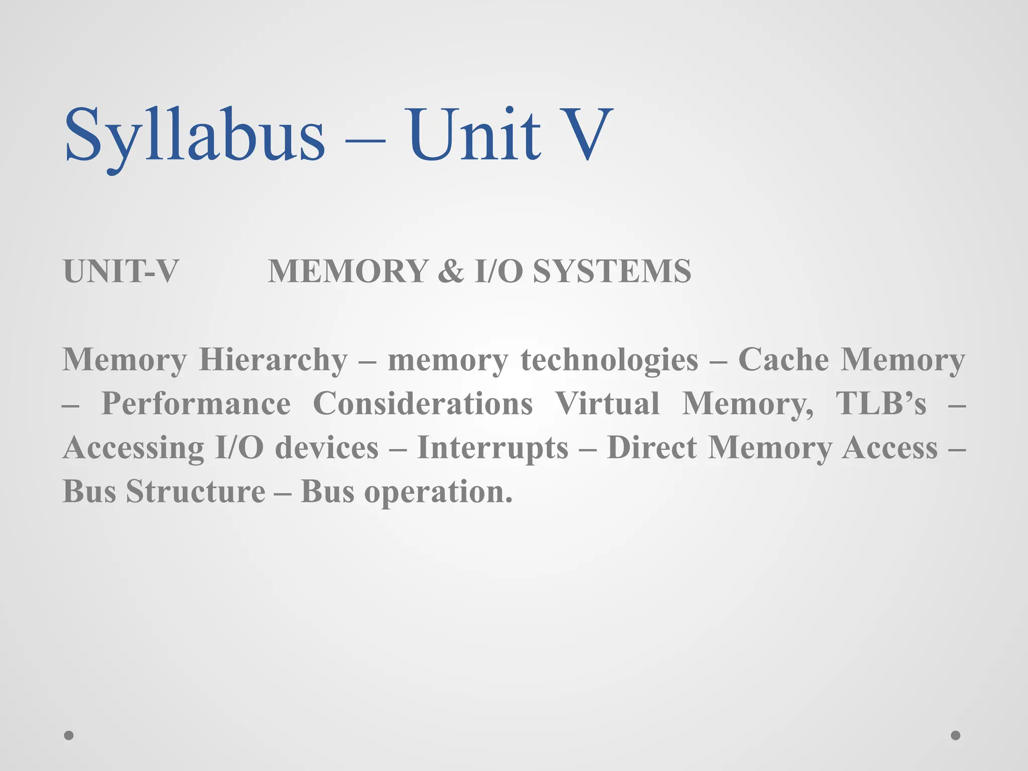
Syllabus – UnitV UNIT-V MEMORY & I/O SYSTEMS Memory Hierarchy – memory technologies – Cache Memory – Performance Considerations Virtual Memory, TLB’s – Accessing I/O devices – Interrupts – Direct Memory Access – Bus Structure – Bus operation.
4.
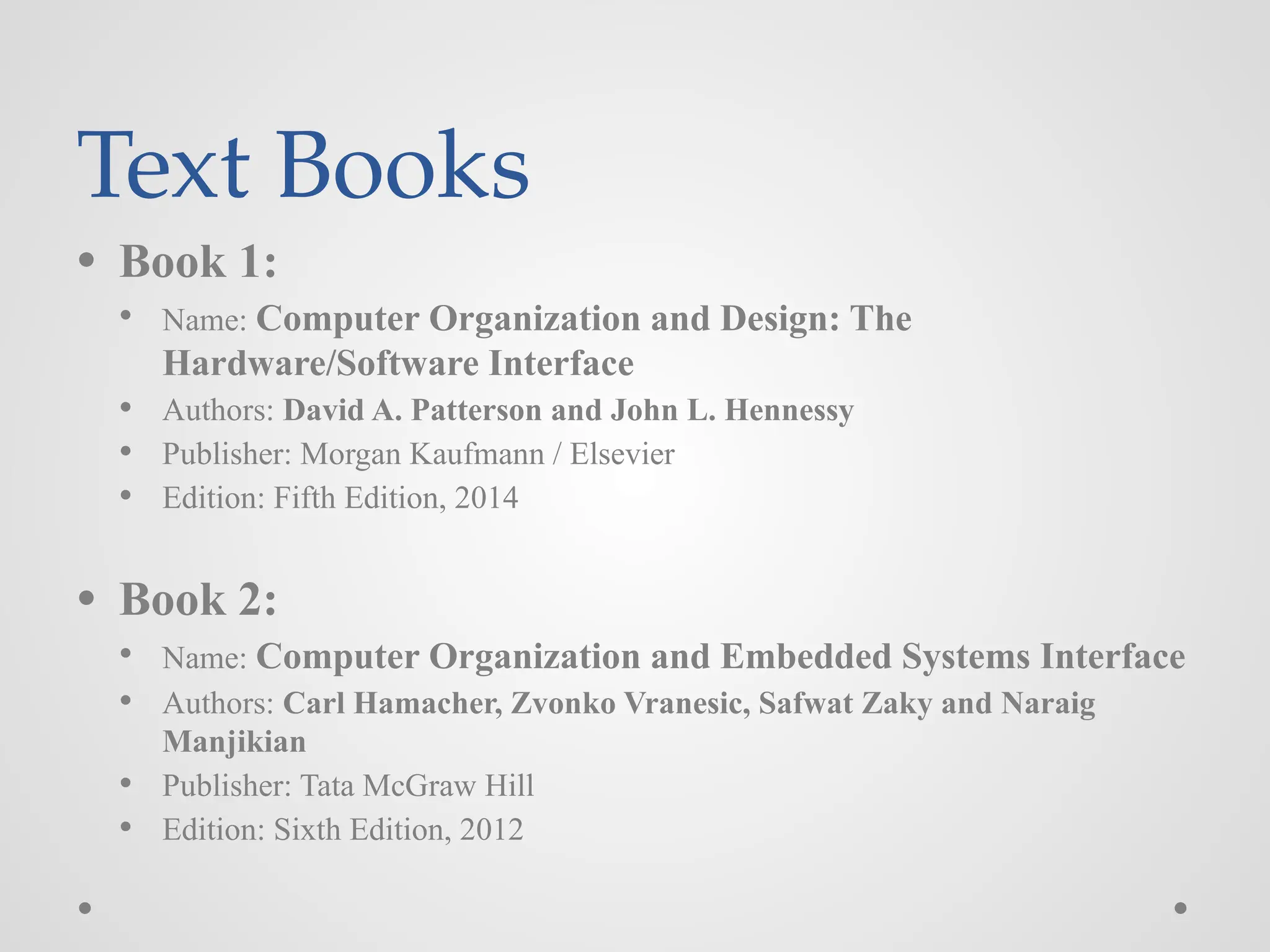
Text Books ● Book1: ● Name: Computer Organization and Design: The Hardware/Software Interface ● Authors: David A. Patterson and John L. Hennessy ● Publisher: Morgan Kaufmann / Elsevier ● Edition: Fifth Edition, 2014 ● Book 2: ● Name: Computer Organization and Embedded Systems Interface ● Authors: Carl Hamacher, Zvonko Vranesic, Safwat Zaky and Naraig Manjikian ● Publisher: Tata McGraw Hill ● Edition: Sixth Edition, 2012
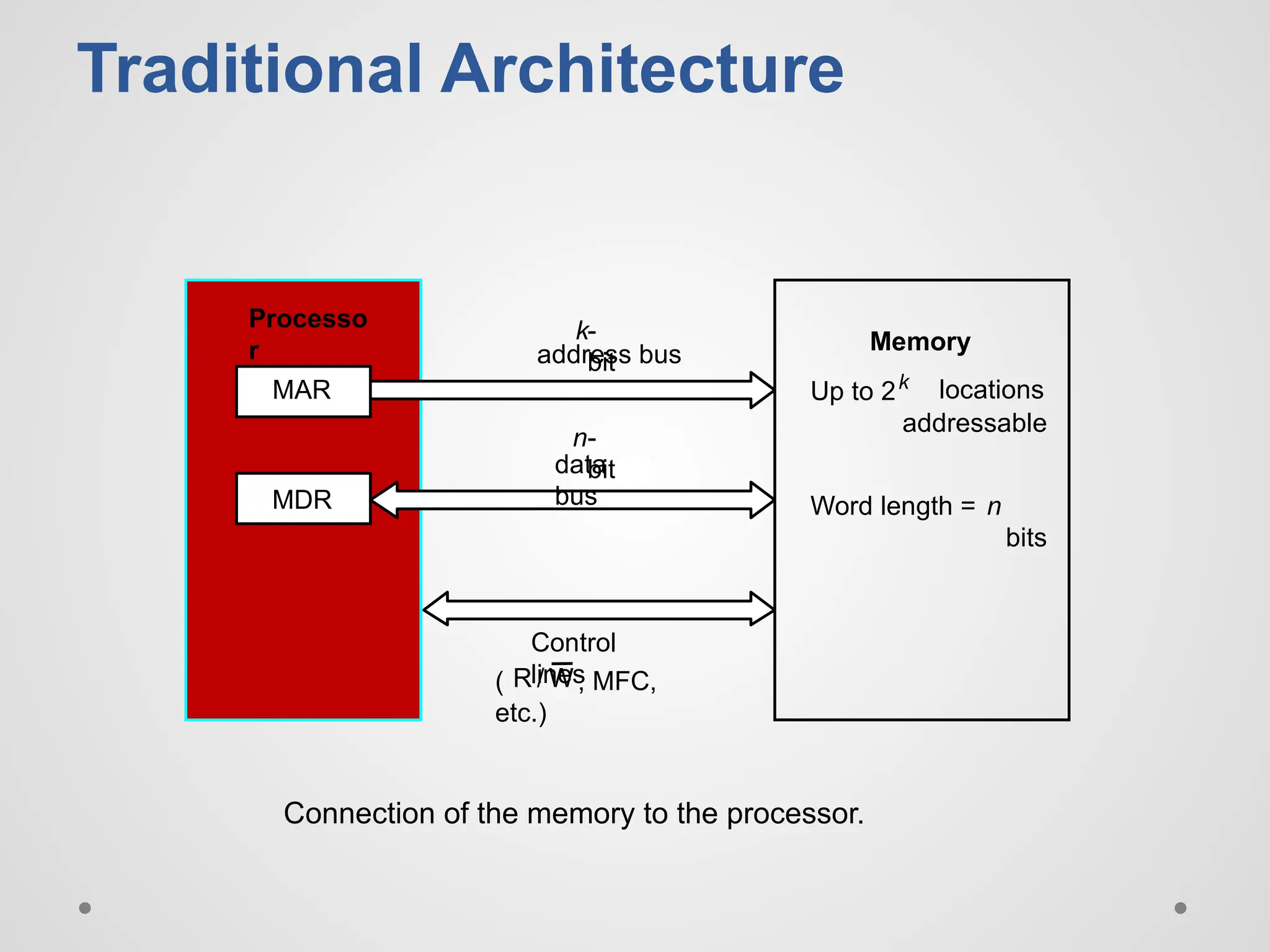
Traditional Architecture Up to2k addressable MDR MAR Connection of the memory to the processor. k- bit address bus n- bit data bus Control lines ( , MFC, etc.) Processo r Memory locations Word length = n bits W R /
9.
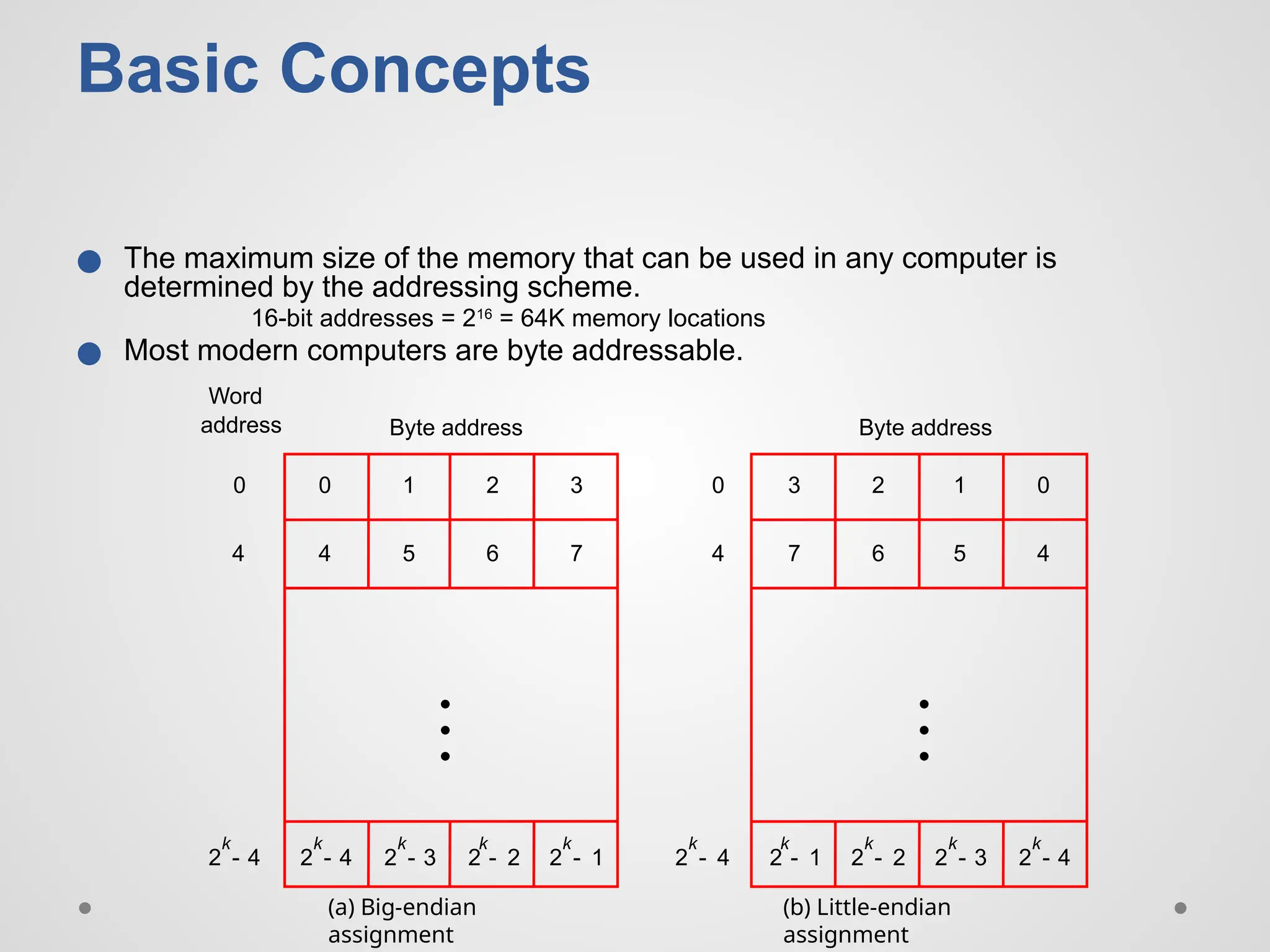
Basic Concepts ● Themaximum size of the memory that can be used in any computer is determined by the addressing scheme. 16-bit addresses = 216 = 64K memory locations ● Most modern computers are byte addressable. 2 k 4 - 2 k 3 - 2 k 2 - 2 k 1 - 2 k 4 - 2 k 4 - 0 1 2 3 4 5 6 7 0 0 4 2 k 1 - 2 k 2 - 2 k 3 - 2 k 4 - 3 2 1 0 7 6 5 4 Byte address Byte address (a) Big-endian assignment (b) Little-endian assignment 4 Word address • • • • • •
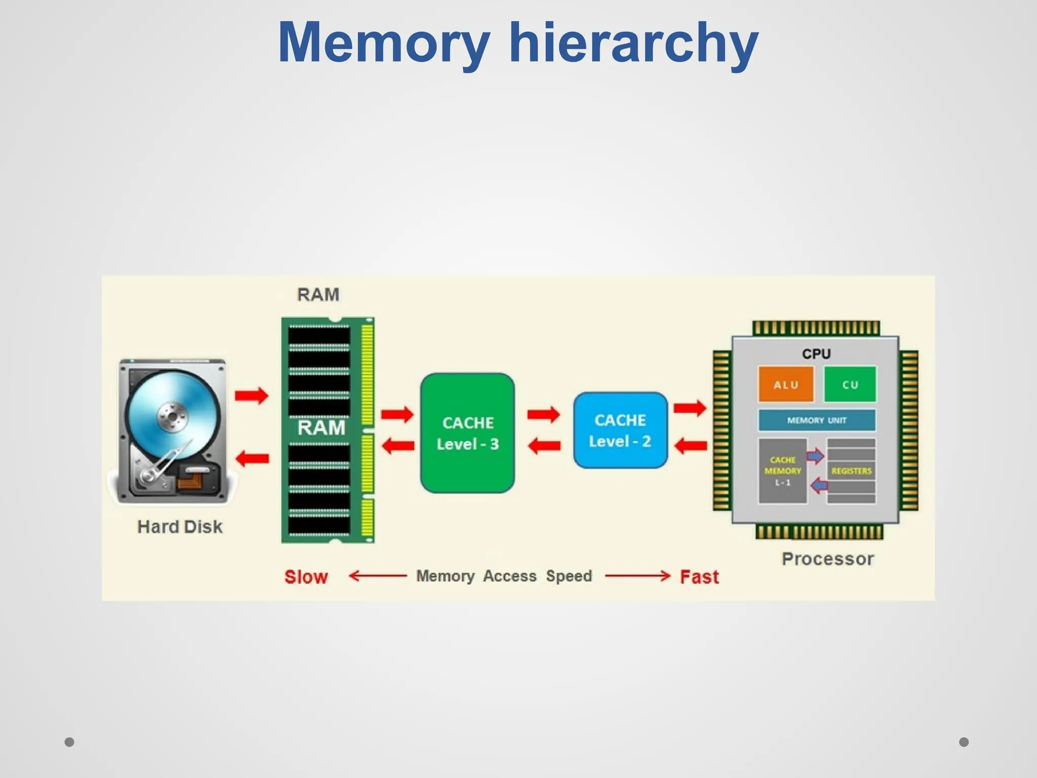
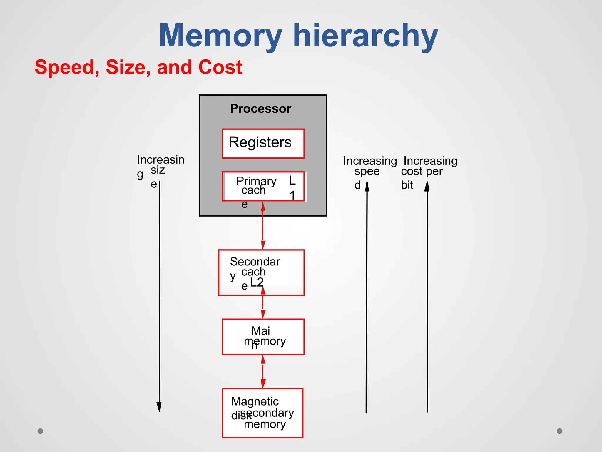
Memory hierarchy ● Astructure that uses multiple levels of memories; as the distance from the processor increases, the size of the memories and the access time both increase.
13.
Speed, Size, andCost Processor Primary cach e Secondar y cach e Mai n Magnetic disk memory Increasin g siz e Increasing spee d Memory hierarchy secondary memory Increasing cost per bit Registers L 1 L2
14.
● Check whetherthe following statements are true not? ● Most of the cost of the memory hierarchy is at the highest level. ● Most of the capacity of the memory hierarchy is at the lowest level.
15.
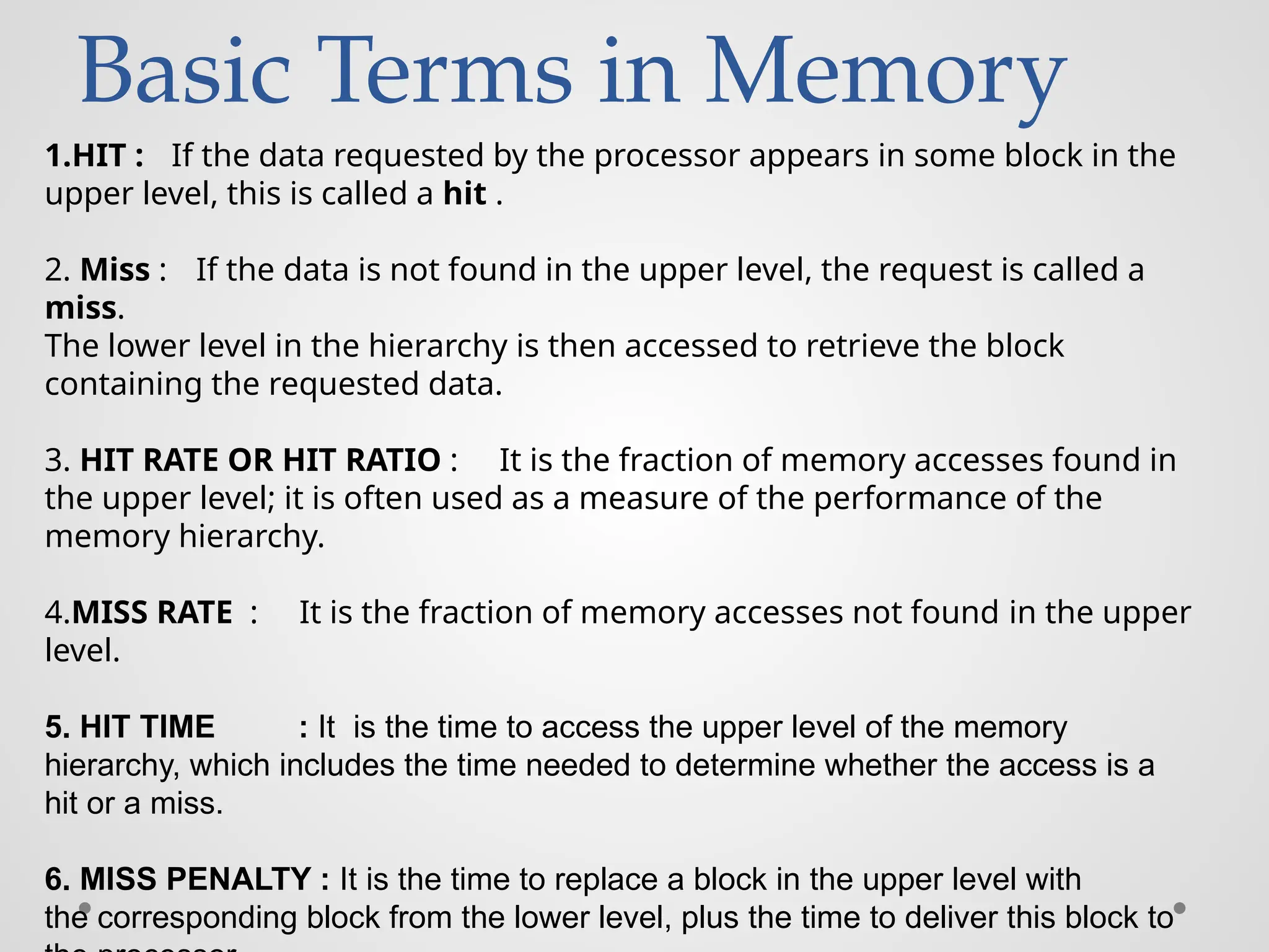
Basic Terms inMemory 1.HIT : If the data requested by the processor appears in some block in the upper level, this is called a hit . 2. Miss : If the data is not found in the upper level, the request is called a miss. The lower level in the hierarchy is then accessed to retrieve the block containing the requested data. 3. HIT RATE OR HIT RATIO : It is the fraction of memory accesses found in the upper level; it is often used as a measure of the performance of the memory hierarchy. 4.MISS RATE : It is the fraction of memory accesses not found in the upper level. 5. HIT TIME : It is the time to access the upper level of the memory hierarchy, which includes the time needed to determine whether the access is a hit or a miss. 6. MISS PENALTY : It is the time to replace a block in the upper level with the corresponding block from the lower level, plus the time to deliver this block to
16.
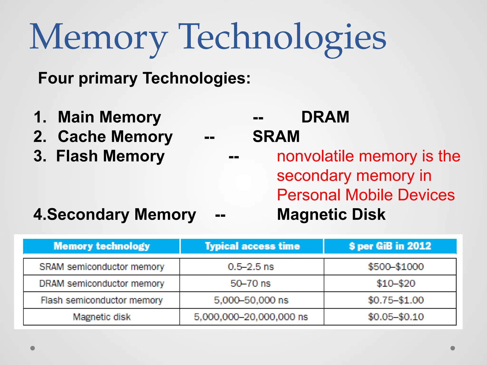
Memory Technologies Four primaryTechnologies: 1. Main Memory -- DRAM 2. Cache Memory -- SRAM 3. Flash Memory -- nonvolatile memory is the secondary memory in Personal Mobile Devices 4.Secondary Memory -- Magnetic Disk
17.
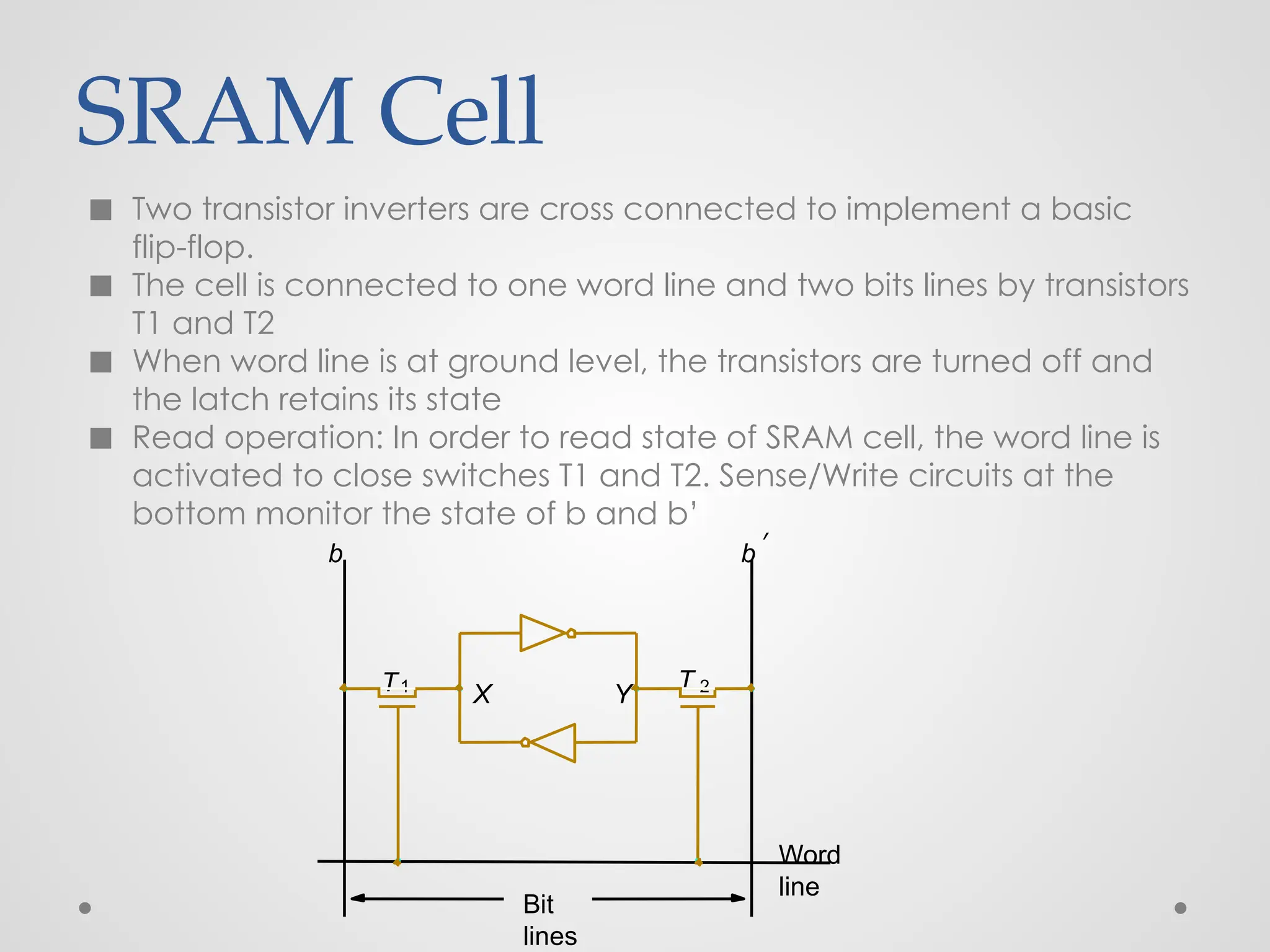
SRAM Cell ◼ Twotransistor inverters are cross connected to implement a basic flip-flop. ◼ The cell is connected to one word line and two bits lines by transistors T1 and T2 ◼ When word line is at ground level, the transistors are turned off and the latch retains its state ◼ Read operation: In order to read state of SRAM cell, the word line is activated to close switches T1 and T2. Sense/Write circuits at the bottom monitor the state of b and b’ Y X Word line Bit lines b T 2 T1 b ′
18.
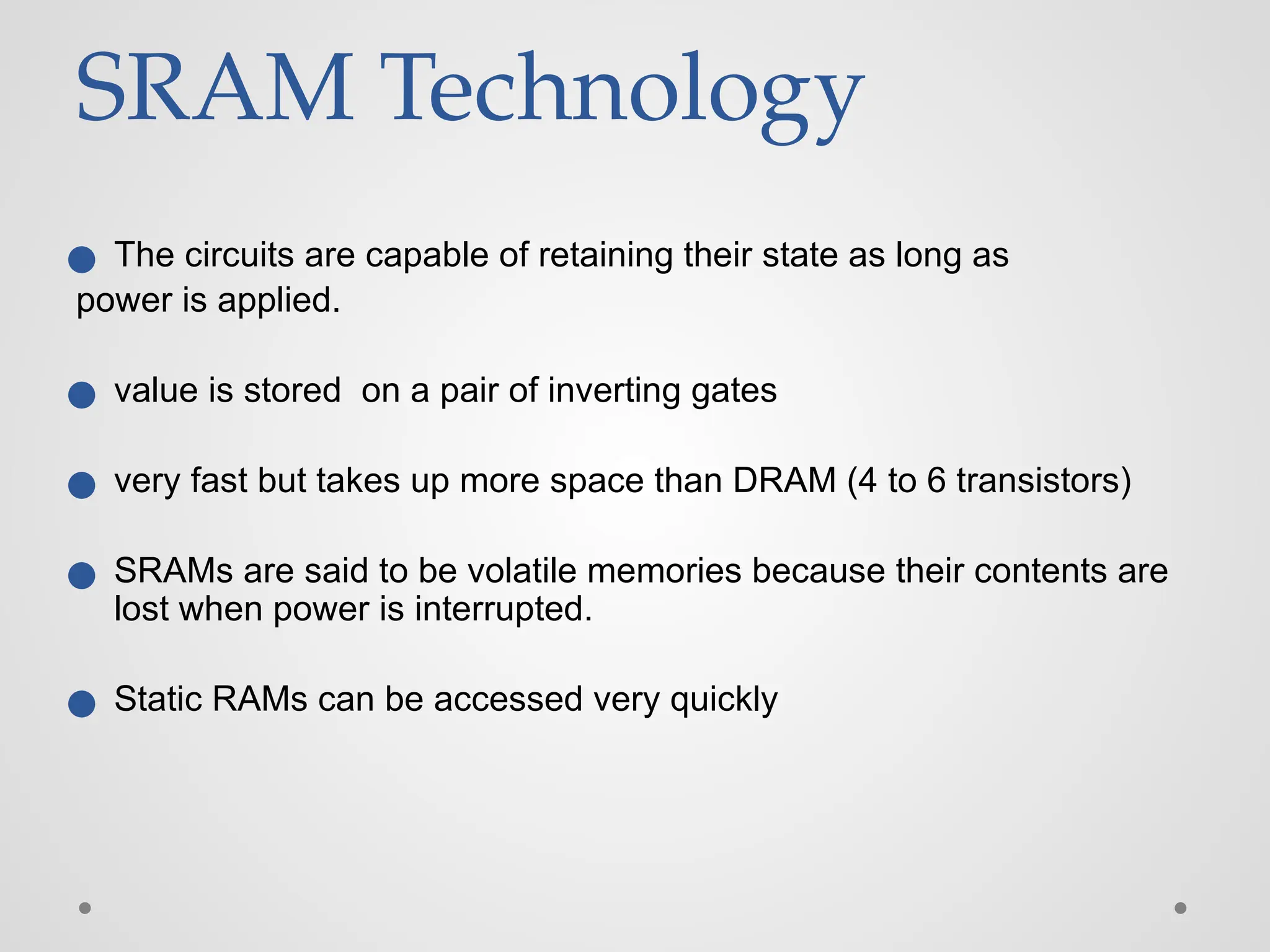
SRAM Technology ● Thecircuits are capable of retaining their state as long as power is applied. ● value is stored on a pair of inverting gates ● very fast but takes up more space than DRAM (4 to 6 transistors) ● SRAMs are said to be volatile memories because their contents are lost when power is interrupted. ● Static RAMs can be accessed very quickly
19.
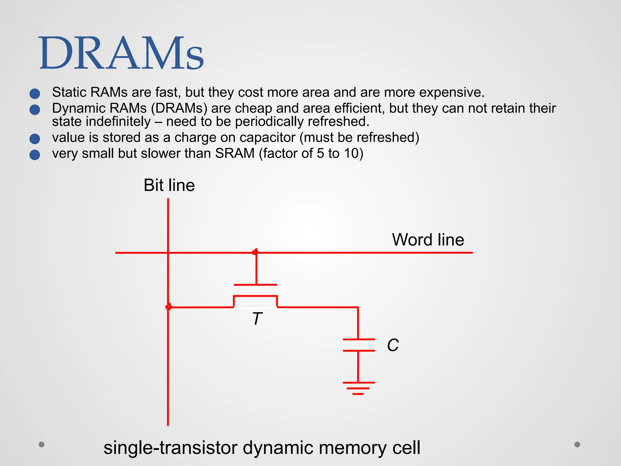
DRAMs ● Static RAMsare fast, but they cost more area and are more expensive. ● Dynamic RAMs (DRAMs) are cheap and area efficient, but they can not retain their state indefinitely – need to be periodically refreshed. ● value is stored as a charge on capacitor (must be refreshed) ● very small but slower than SRAM (factor of 5 to 10) single-transistor dynamic memory cell T C Word line Bit line
20.
◼ Static RAMs(SRAMs): ▪ Consist of circuits that are capable of retaining their state as long as the power is applied. ▪ Volatile memories, because their contents are lost when power is interrupted. ▪ Access times of static RAMs are in the range of few nanoseconds. ▪ However, the cost is usually high. ◼ Dynamic RAMs (DRAMs): ▪ Do not retain their state indefinitely. ▪ Contents must be periodically refreshed. ▪ Contents may be refreshed while accessing them for reading.
21.
Questions ◼ What ismean by memory hierarchy? ◼ What are the factors to be considered in memory hierarchy? ◼ Define hit and miss. ◼ Comparison between SRAM and DRAM.
22.
Latency & Bandwidth ◼Memory latency is the time it takes to transfer a word of data to or from memory ◼ Memory bandwidth is the number of bits or bytes that can be transferred in one second.
23.
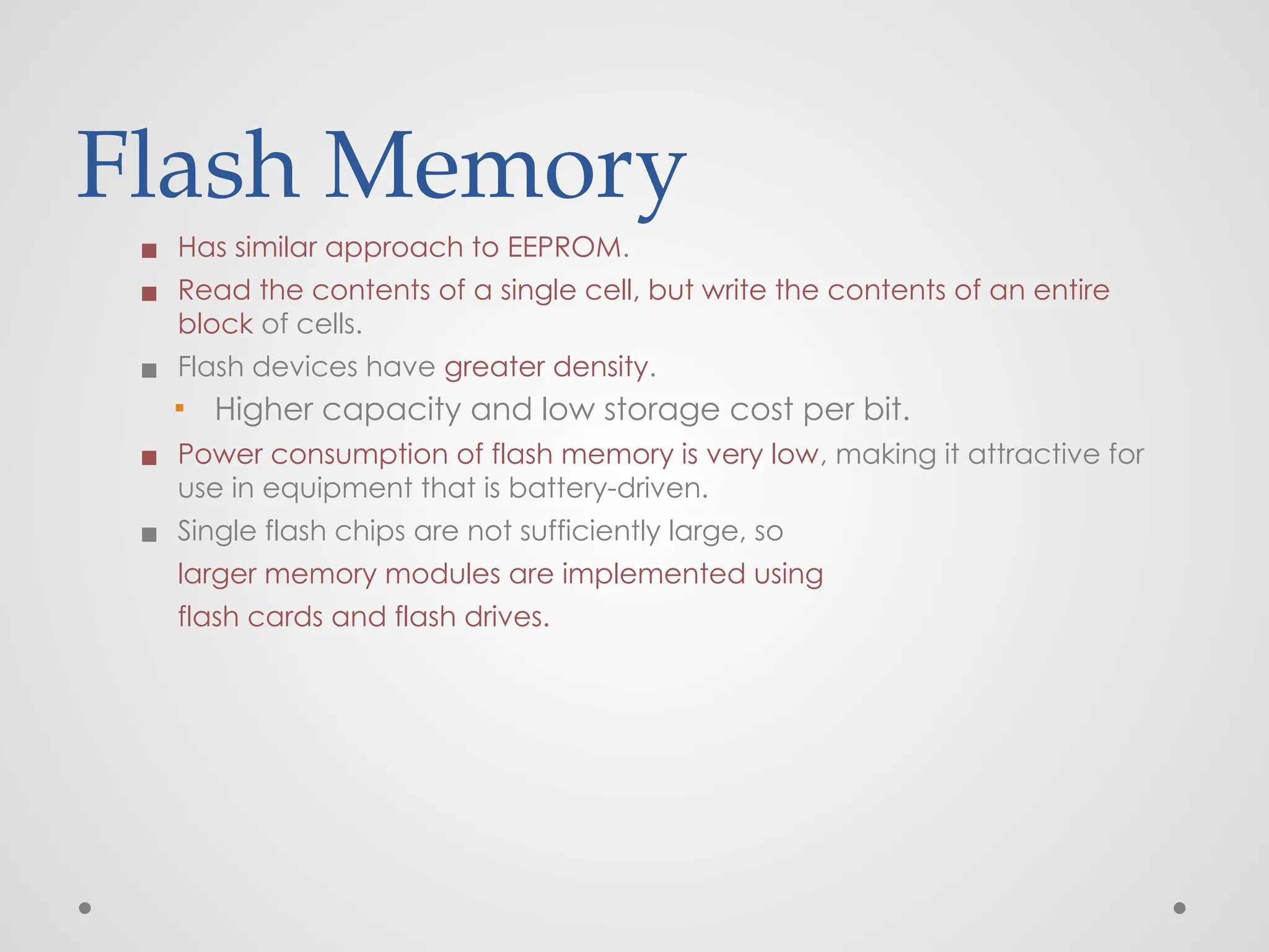
Flash Memory ▪ Hassimilar approach to EEPROM. ▪ Read the contents of a single cell, but write the contents of an entire block of cells. ▪ Flash devices have greater density. ▪ Higher capacity and low storage cost per bit. ▪ Power consumption of flash memory is very low, making it attractive for use in equipment that is battery-driven. ▪ Single flash chips are not sufficiently large, so larger memory modules are implemented using flash cards and flash drives.
24.
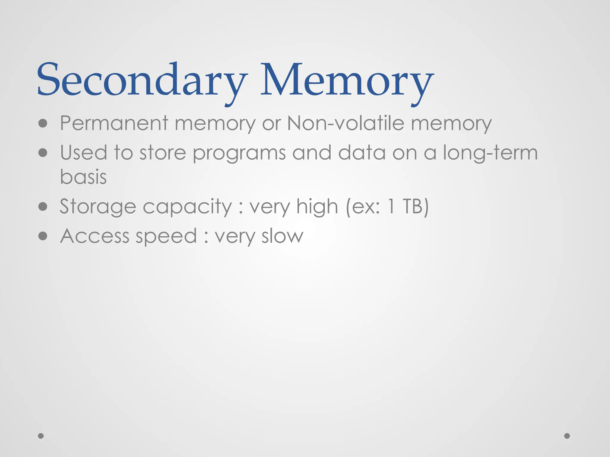
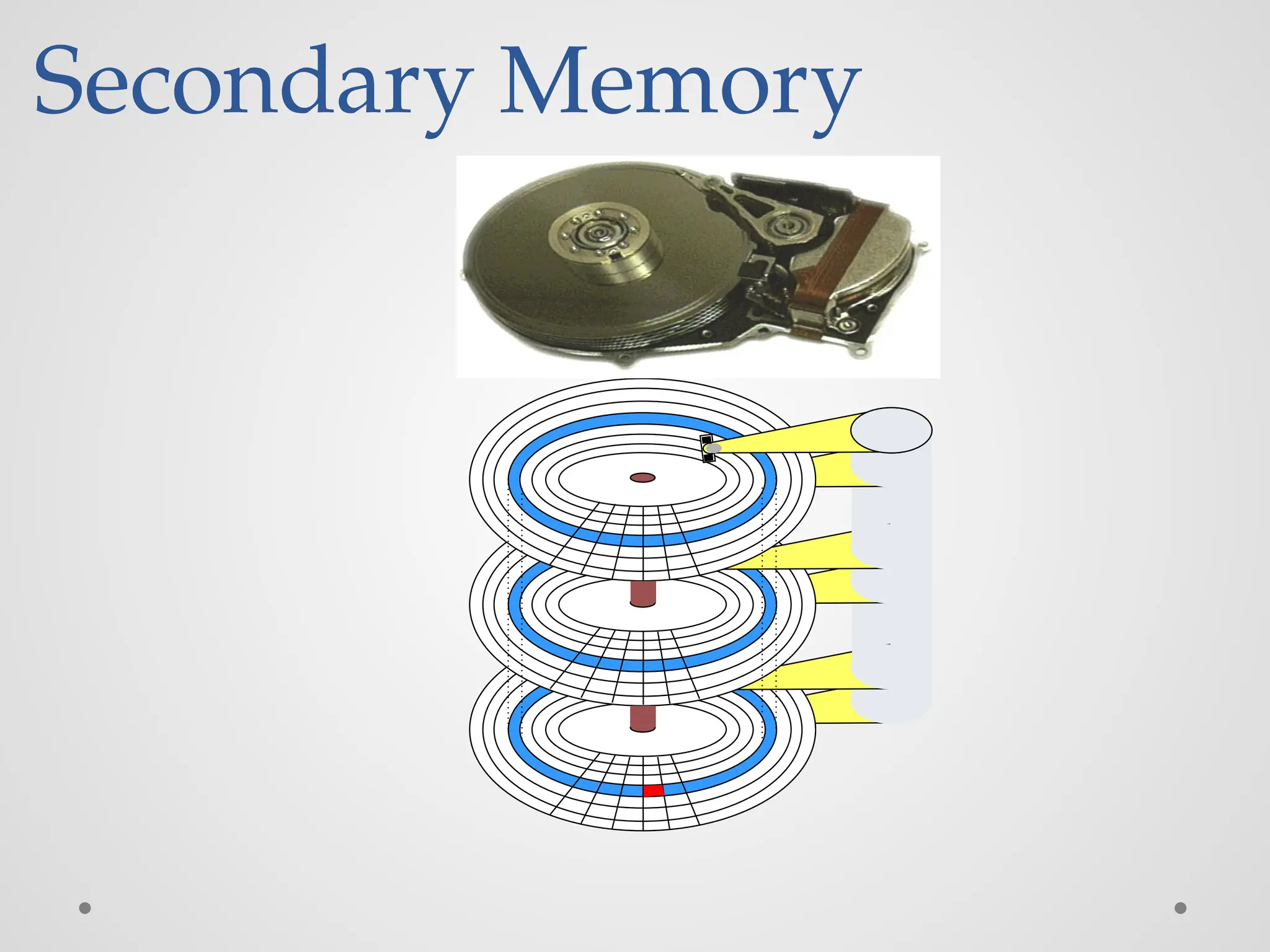
Secondary Memory ● Permanentmemory or Non-volatile memory ● Used to store programs and data on a long-term basis ● Storage capacity : very high (ex: 1 TB) ● Access speed : very slow
25.
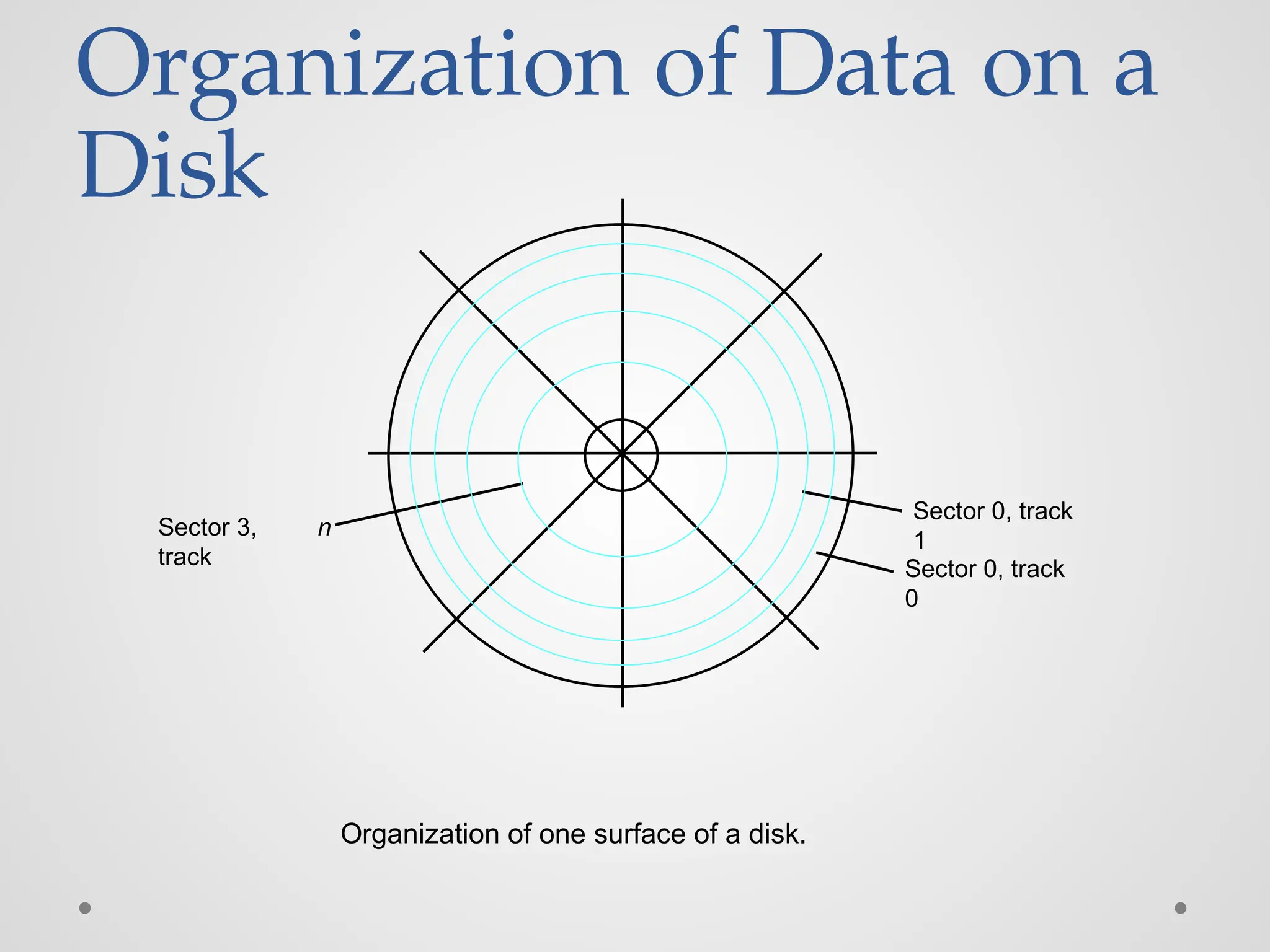
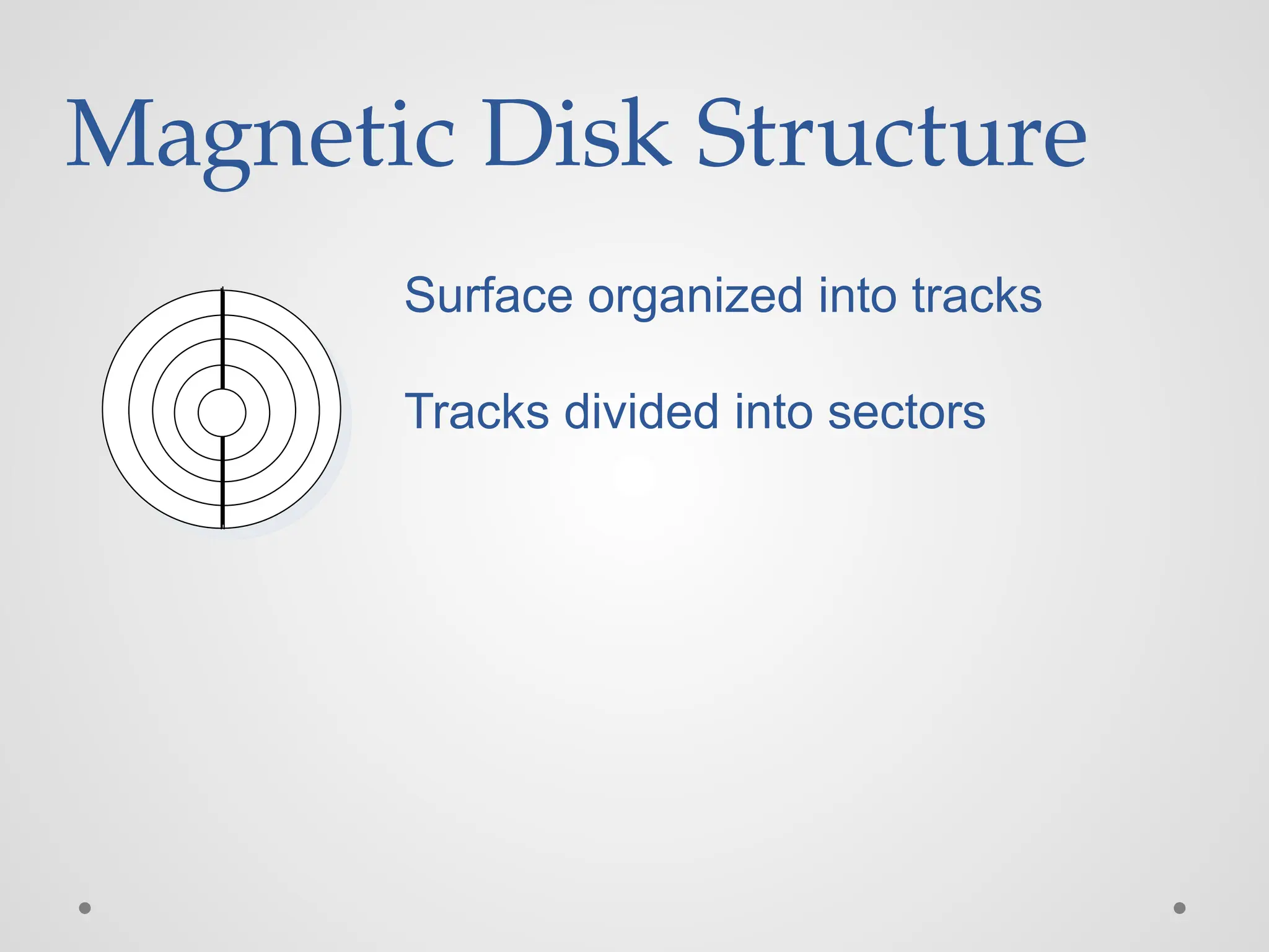
Organization of Dataon a Disk Sector 0, track 0 Sector 3, track n Organization of one surface of a disk. Sector 0, track 1
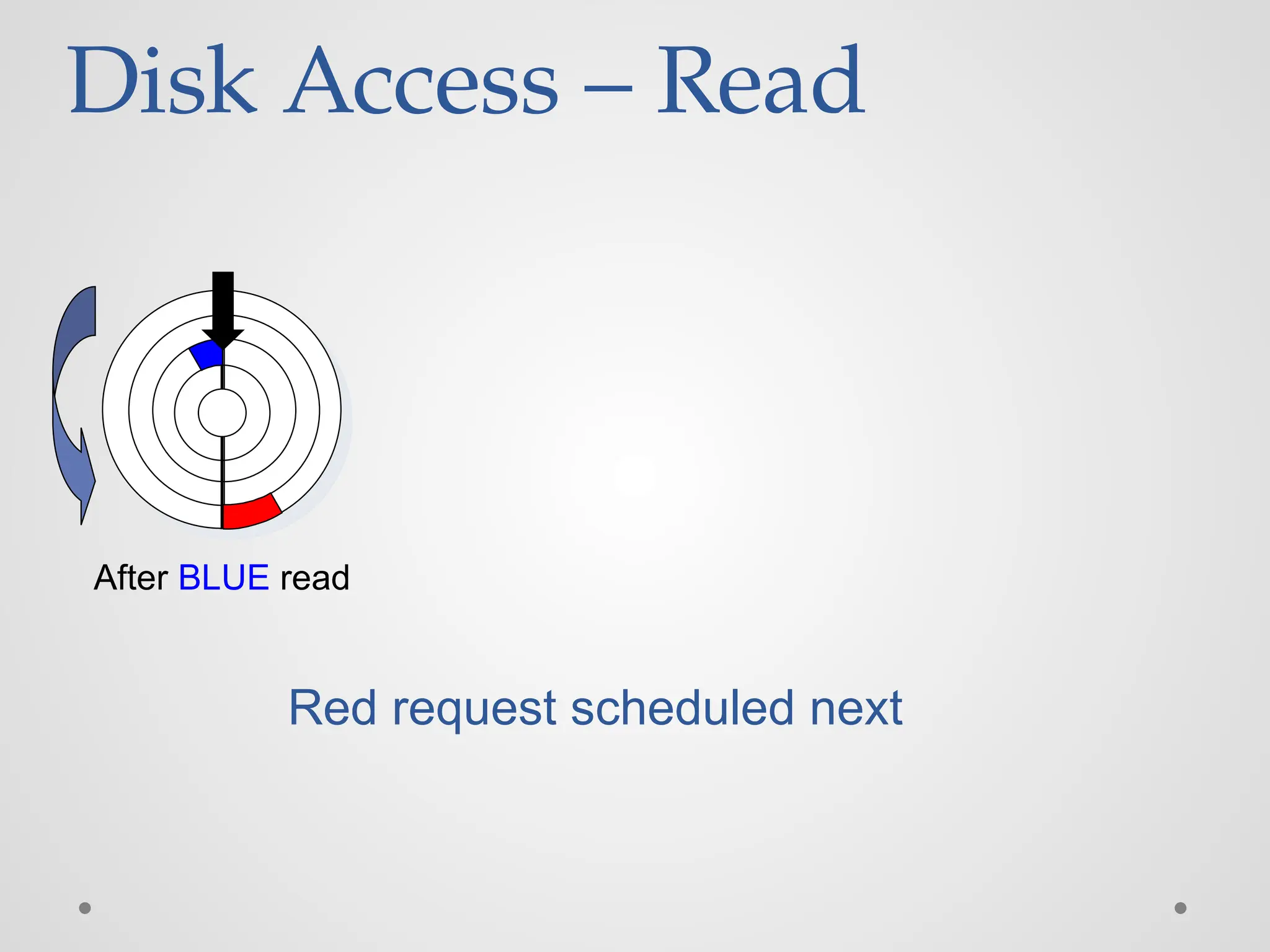
Disk Access –Read After BLUE read After reading blue sector
32.
Disk Access –Read After BLUE read Red request scheduled next
33.
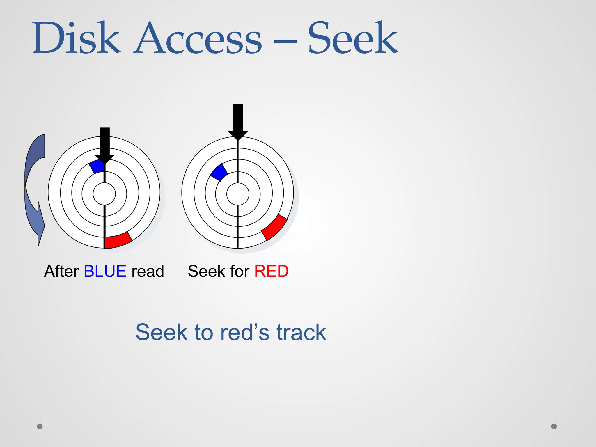
Disk Access –Seek After BLUE read Seek for RED Seek to red’s track
34.
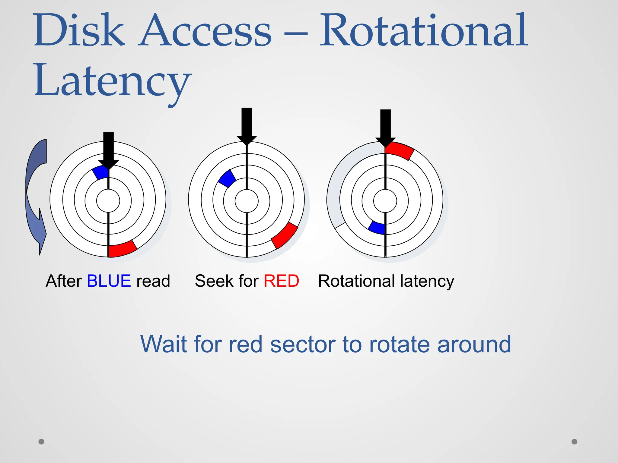
Disk Access –Rotational Latency After BLUE read Seek for RED Rotational latency Wait for red sector to rotate around
35.
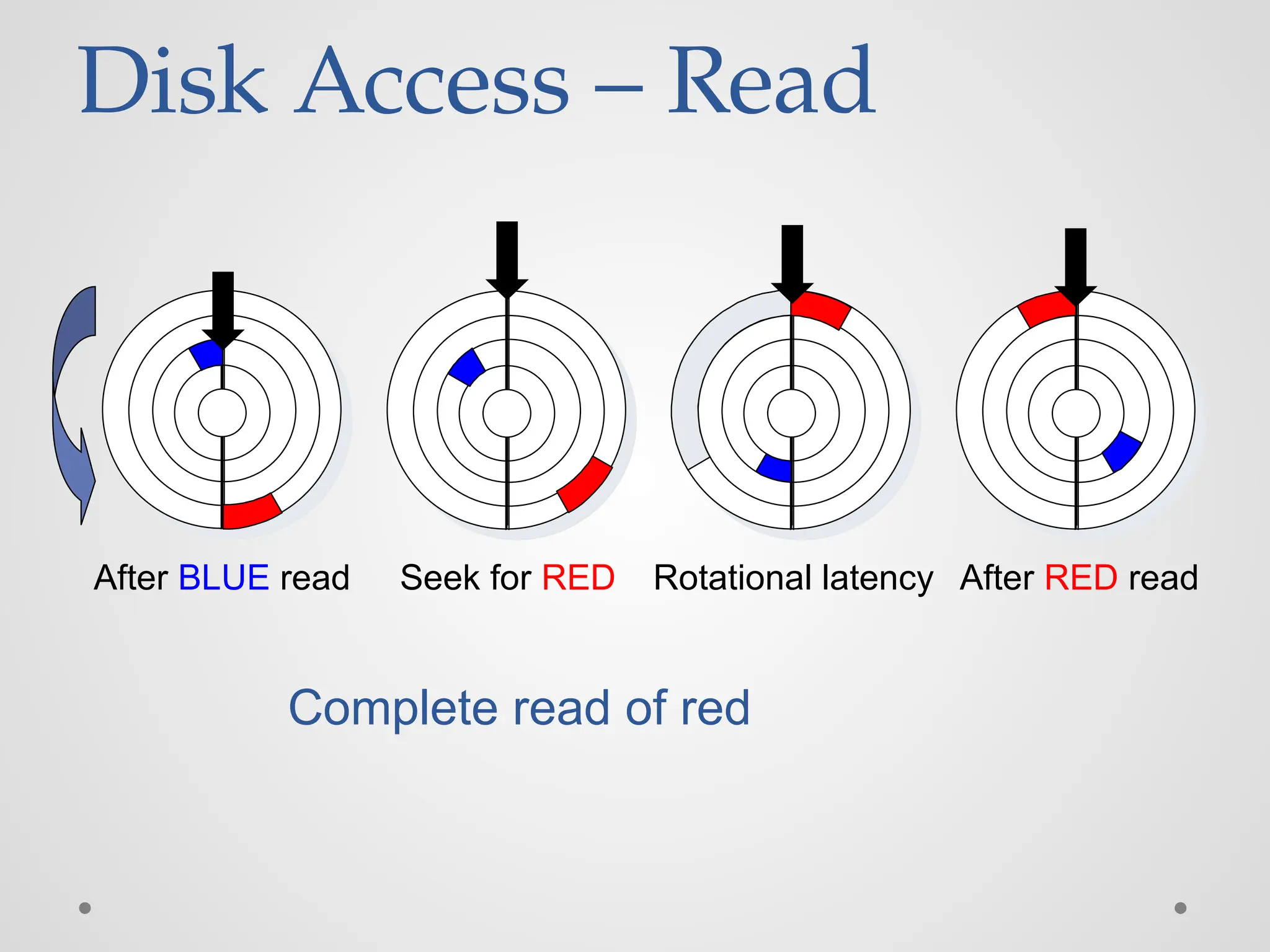
Disk Access –Read After BLUE read Seek for RED Rotational latency After RED read Complete read of red
36.
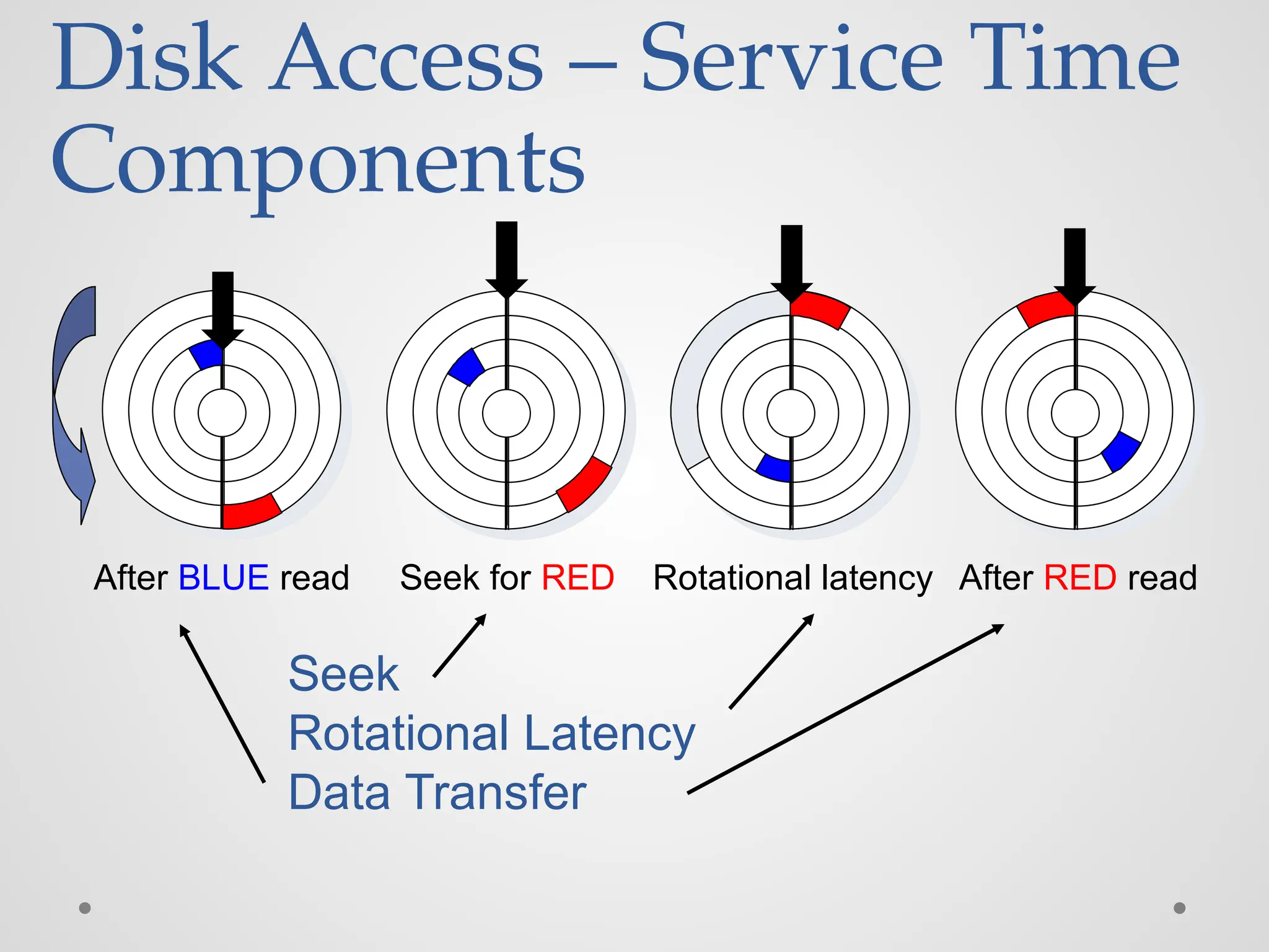
Disk Access –Service Time Components After BLUE read Seek for RED Rotational latency After RED read Seek Rotational Latency Data Transfer
37.
Speed, Size, andCost ◼ A big challenge in the design of a computer system is to provide a sufficiently large memory, with a reasonable speed at an affordable cost. ◼ Static RAM: ▪ Very fast, but expensive, because a basic SRAM cell has a complex circuit making it impossible to pack a large number of cells onto a single chip. ◼ Dynamic RAM: ▪ Simpler basic cell circuit, hence are much less expensive, but significantly slower than SRAMs. ◼ Magnetic disks: ▪ Storage provided by DRAMs is higher than SRAMs, but is still less than what is necessary. ▪ Secondary storage such as magnetic disks provide a large amount of storage, but is much slower than DRAMs.
Cache ● What iscache memory? ● Why we need it? ● Locality of reference (very important) - temporal - spatial ● Cache block – cache line ● A set of contiguous address locations of some size
40.
What is cachememory? ● The cache memory is a small-sized high speed volatile memory that provides high speed data access to a processor. ● The cache memory stores the frequently used computer programs, applications and the program data.
41.
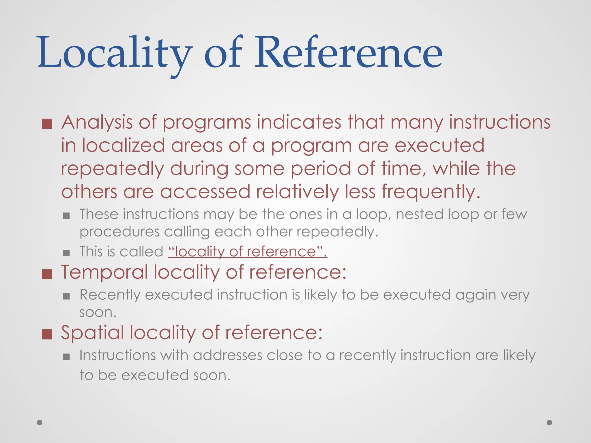
Locality of Reference ◼Analysis of programs indicates that many instructions in localized areas of a program are executed repeatedly during some period of time, while the others are accessed relatively less frequently. ▪ These instructions may be the ones in a loop, nested loop or few procedures calling each other repeatedly. ▪ This is called “locality of reference”. ◼ Temporal locality of reference: ▪ Recently executed instruction is likely to be executed again very soon. ◼ Spatial locality of reference: ▪ Instructions with addresses close to a recently instruction are likely to be executed soon.
42.
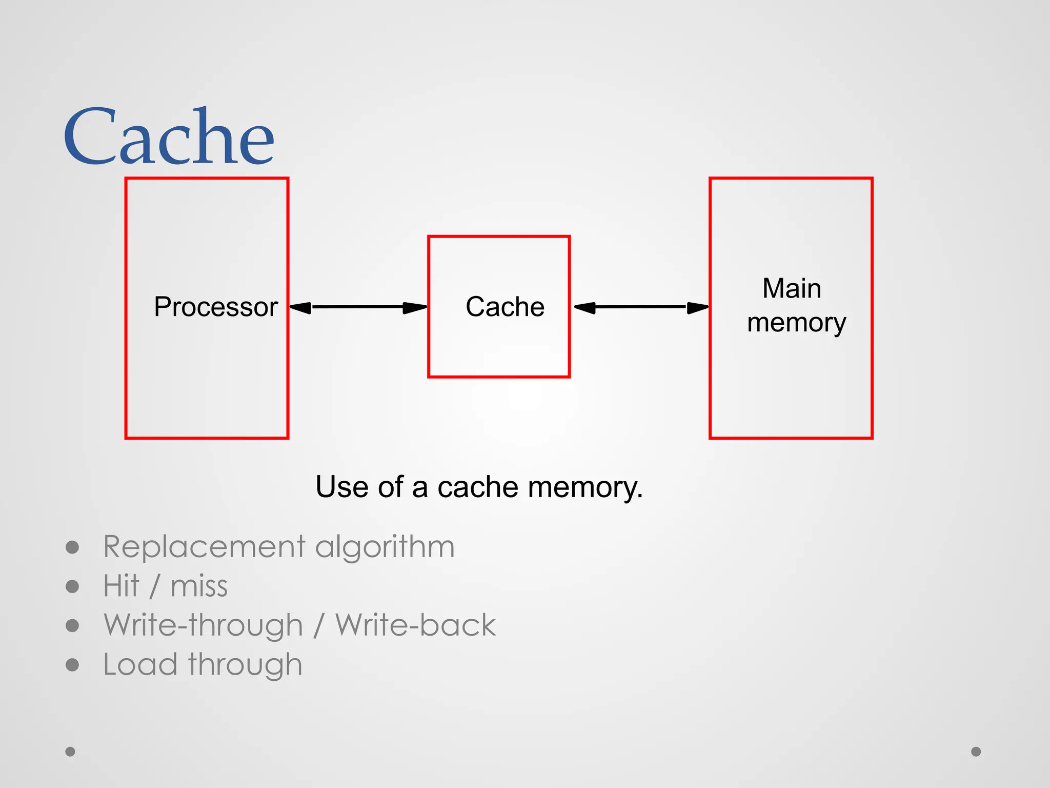
Cache ● Replacement algorithm ●Hit / miss ● Write-through / Write-back ● Load through Use of a cache memory. Cache Main memory Processor
43.
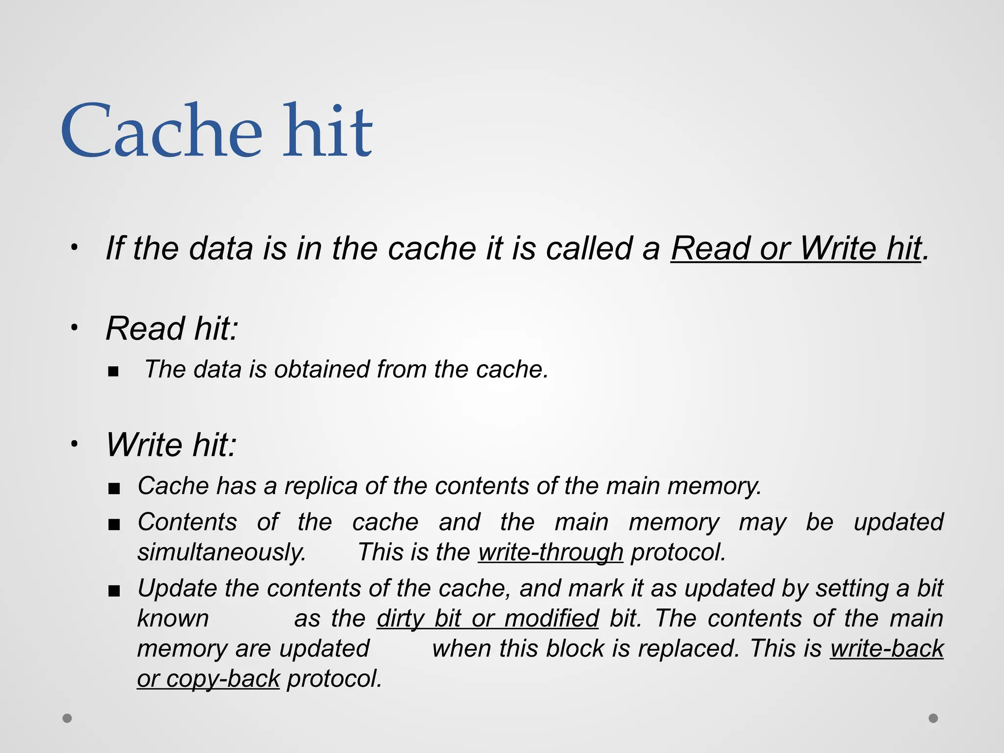
Cache hit • Ifthe data is in the cache it is called a Read or Write hit. • Read hit: ▪ The data is obtained from the cache. • Write hit: ▪ Cache has a replica of the contents of the main memory. ▪ Contents of the cache and the main memory may be updated simultaneously. This is the write-through protocol. ▪ Update the contents of the cache, and mark it as updated by setting a bit known as the dirty bit or modified bit. The contents of the main memory are updated when this block is replaced. This is write-back or copy-back protocol.
44.
Cache miss • Ifthe data is not present in the cache, then a Read miss or Write miss occurs. • Read miss: ▪ Block of words containing this requested word is transferred from the memory. ▪ After the block is transferred, the desired word is forwarded to the processor. ▪ The desired word may also be forwarded to the processor as soon as it is transferred without waiting for the entire block to be transferred. This is called load-through or early-restart. • Write-miss: ▪ Write-through protocol is used, then the contents of the main memory are updated directly. ▪ If write-back protocol is used, the block containing the addressed word is first brought into the cache. The desired word is overwritten with new information.
45.
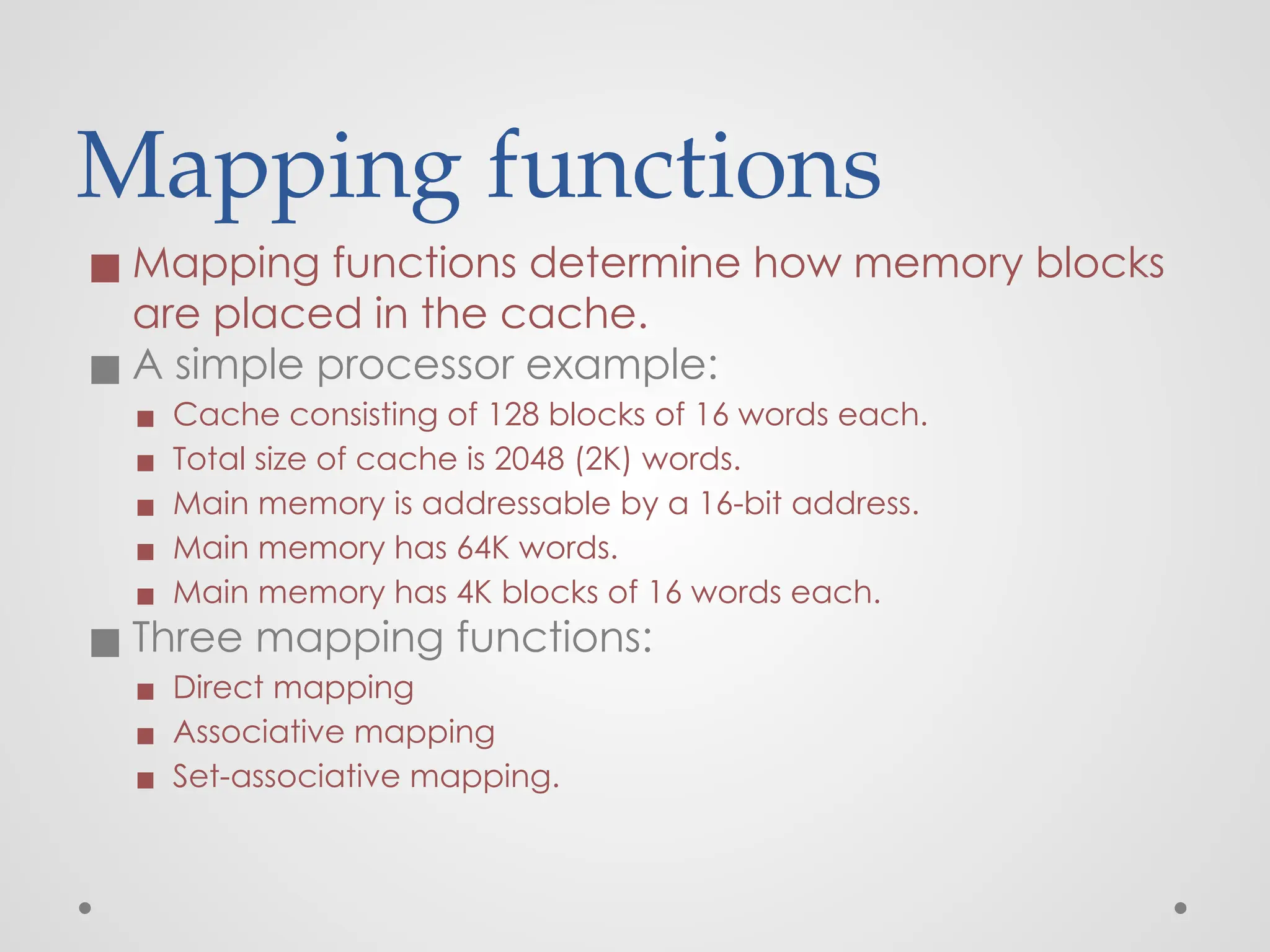
Mapping functions ◼ Mappingfunctions determine how memory blocks are placed in the cache. ◼ A simple processor example: ▪ Cache consisting of 128 blocks of 16 words each. ▪ Total size of cache is 2048 (2K) words. ▪ Main memory is addressable by a 16-bit address. ▪ Main memory has 64K words. ▪ Main memory has 4K blocks of 16 words each. ◼ Three mapping functions: ▪ Direct mapping ▪ Associative mapping ▪ Set-associative mapping.
46.
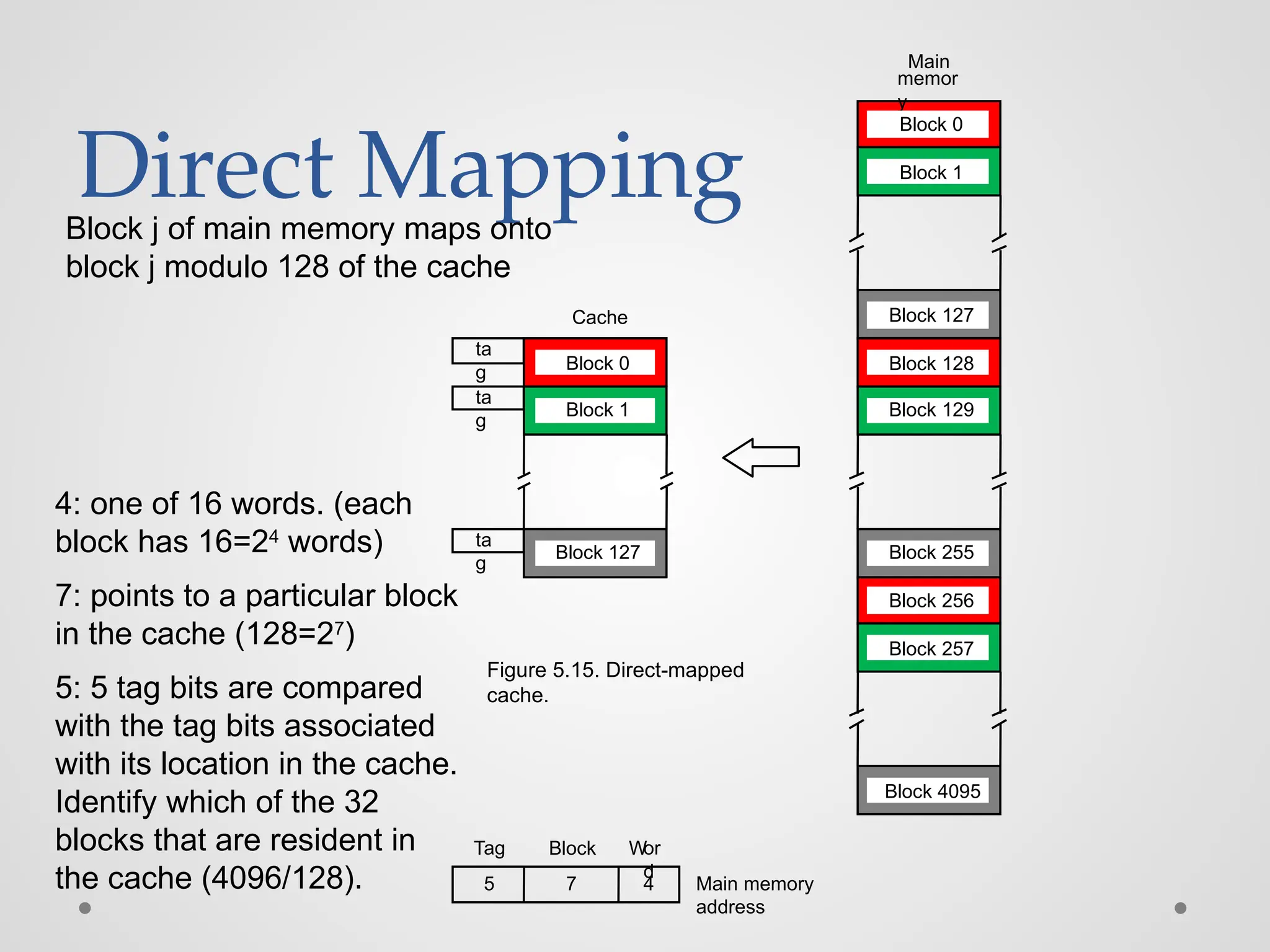
Direct Mapping ta g ta g ta g Cache Main memor y Block 0 Block1 Block 127 Block 128 Block 129 Block 255 Block 256 Block 257 Block 4095 Block 0 Block 1 Block 127 7 4 Main memory address Tag Block Wor d Figure 5.15. Direct-mapped cache. 5 4: one of 16 words. (each block has 16=24 words) 7: points to a particular block in the cache (128=27 ) 5: 5 tag bits are compared with the tag bits associated with its location in the cache. Identify which of the 32 blocks that are resident in the cache (4096/128). Block j of main memory maps onto block j modulo 128 of the cache
47.
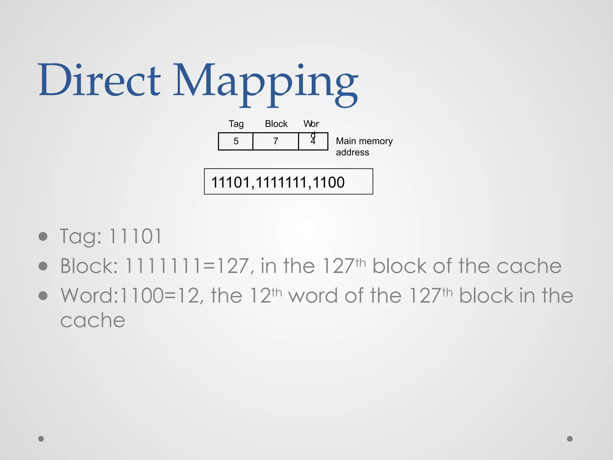
Direct Mapping ● Tag:11101 ● Block: 1111111=127, in the 127th block of the cache ● Word:1100=12, the 12th word of the 127th block in the cache 7 4 Main memory address Tag Block Wor d 5 11101,1111111,1100
48.
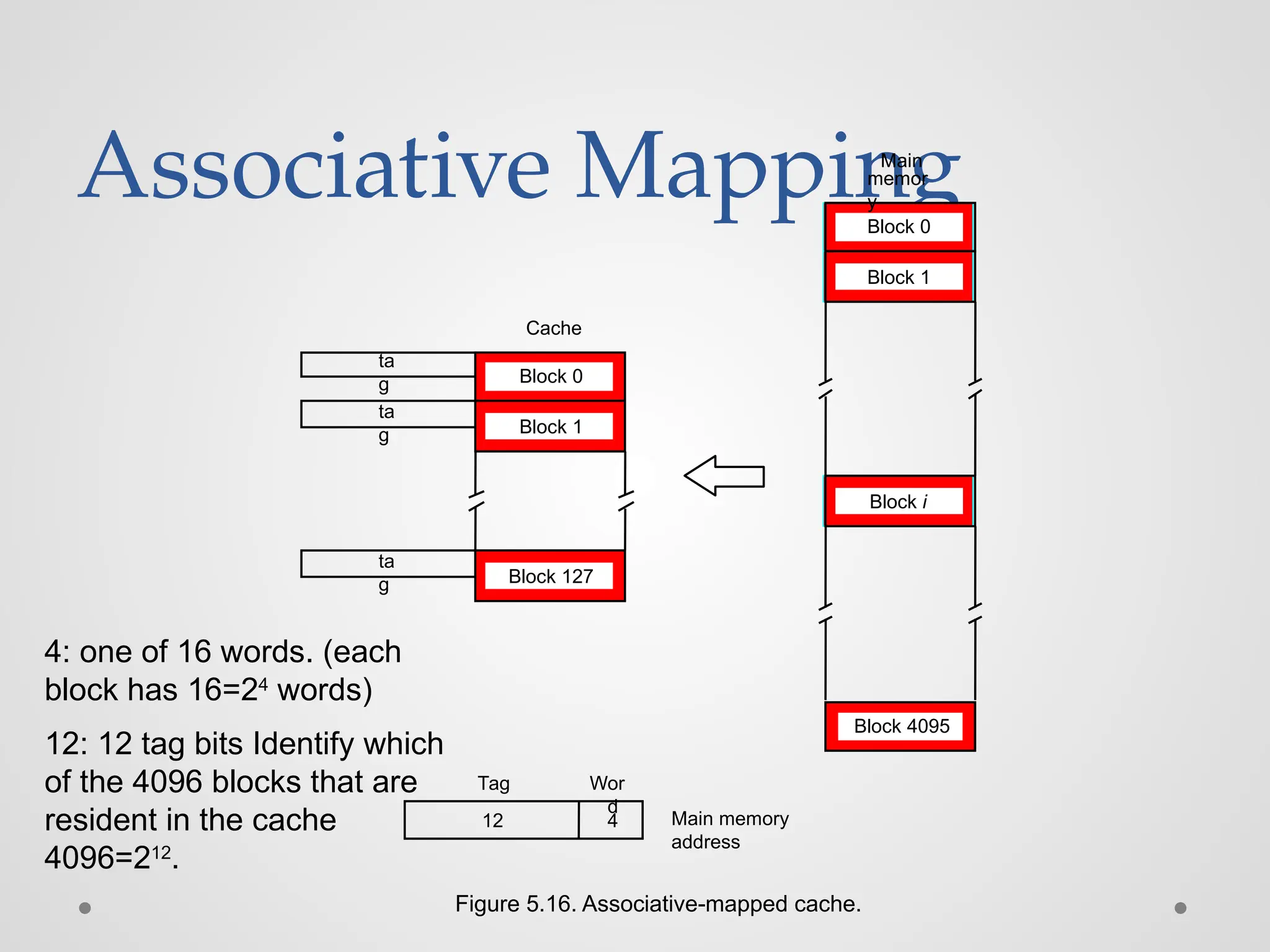
Associative Mapping 4 ta g ta g ta g Cache Main memor y Block 0 Block1 Block i Block 4095 Block 0 Block 1 Block 127 12 Main memory address Figure 5.16. Associative-mapped cache. Tag Wor d 4: one of 16 words. (each block has 16=24 words) 12: 12 tag bits Identify which of the 4096 blocks that are resident in the cache 4096=212 .
49.
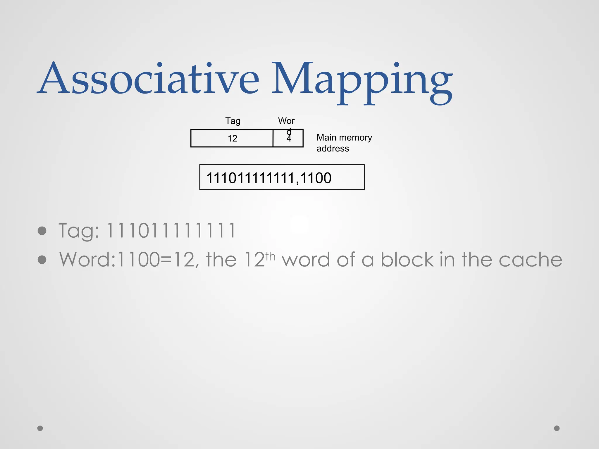
Associative Mapping ● Tag:111011111111 ● Word:1100=12, the 12th word of a block in the cache 111011111111,1100 4 12 Main memory address Tag Wor d
50.
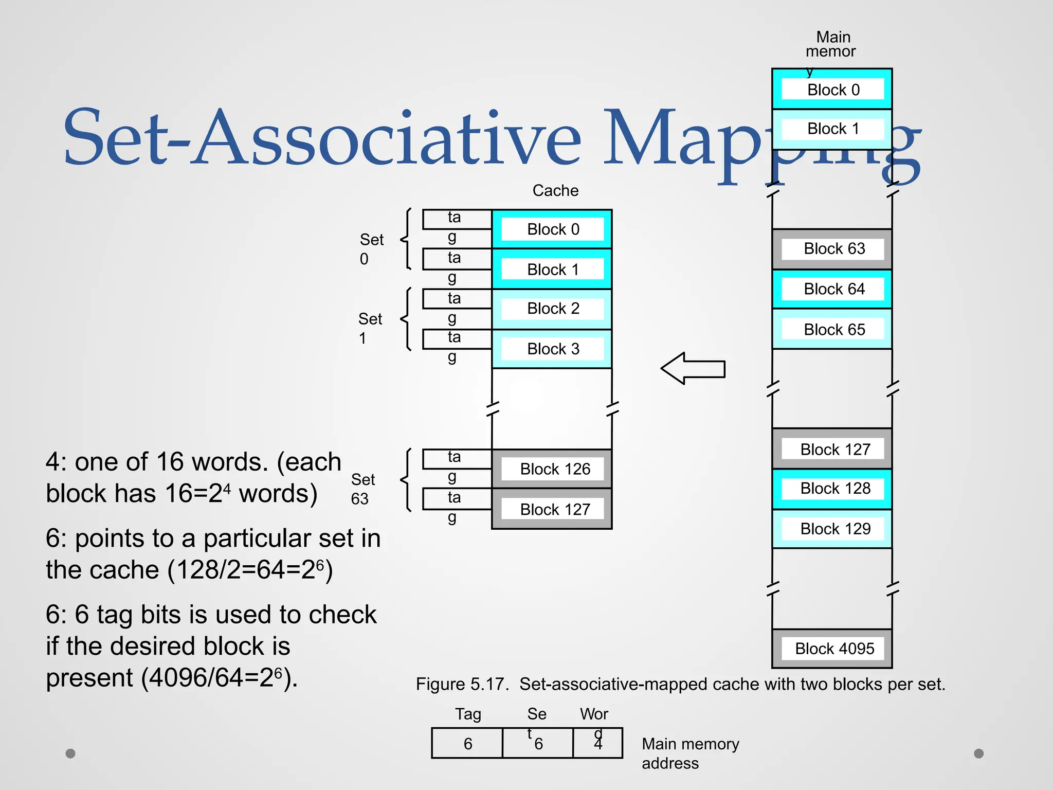
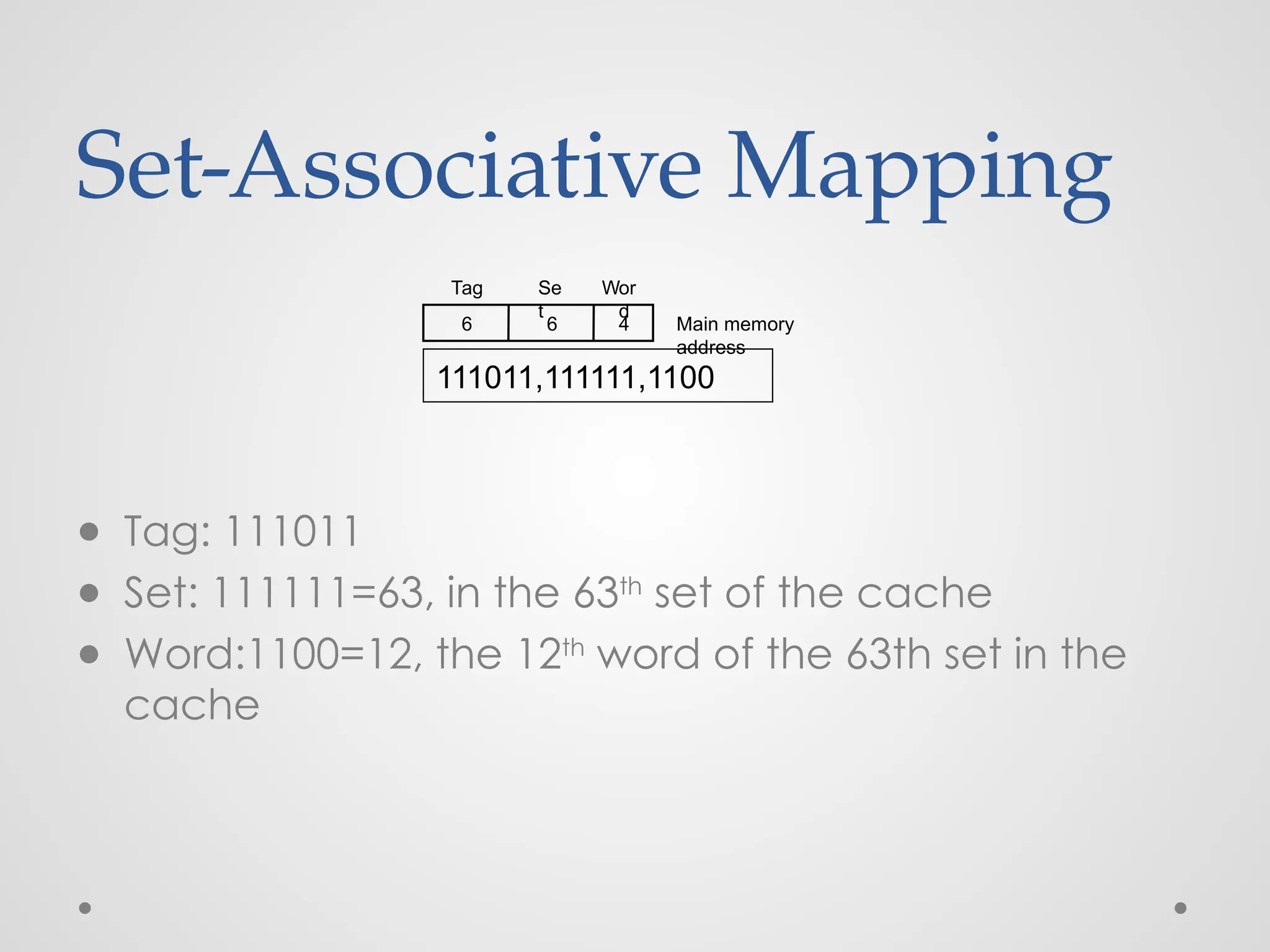
Set-Associative Mapping ta g ta g ta g Cache Main memor y Block 0 Block1 Block 63 Block 64 Block 65 Block 127 Block 128 Block 129 Block 4095 Block 0 Block 1 Block 126 ta g ta g Block 2 Block 3 ta g Block 127 Main memory address 6 6 4 Tag Se t Wor d Set 0 Set 1 Set 63 Figure 5.17. Set-associative-mapped cache with two blocks per set. 4: one of 16 words. (each block has 16=24 words) 6: points to a particular set in the cache (128/2=64=26 ) 6: 6 tag bits is used to check if the desired block is present (4096/64=26 ).
51.
Set-Associative Mapping ● Tag:111011 ● Set: 111111=63, in the 63th set of the cache ● Word:1100=12, the 12th word of the 63th set in the cache Main memory address 6 6 4 Tag Se t Wor d 111011,111111,1100
52.
Replacement Algorithms ● Difficultto determine which blocks to kick out ● Least Recently Used (LRU) block ● The cache controller tracks references to all blocks as computation proceeds. ● Increase / clear track counters when a hit/miss occurs
53.
● List outthe mapping functions. ● What is mean by cache memory?
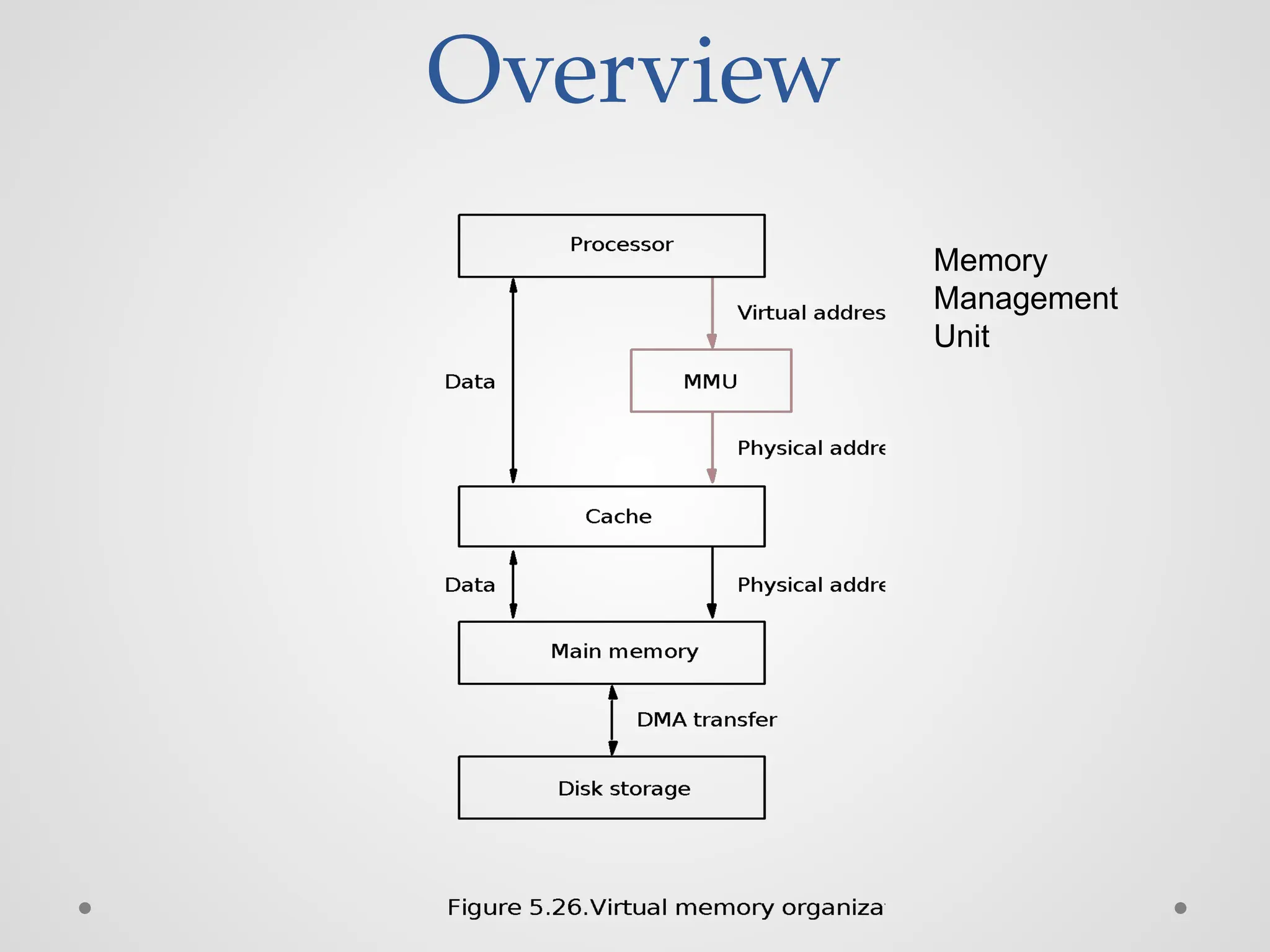
Overview ● Physical mainmemory is not as large as the address space spanned by an address issued by the processor. 232 = 4 GB, 264 = … ● When a program does not completely fit into the main memory, the parts of it not currently being executed are stored on secondary storage devices. ● Techniques that automatically move program and data blocks into the physical main memory when they are required for execution are called virtual-memory techniques. ● Virtual addresses will be translated into physical addresses.
56.
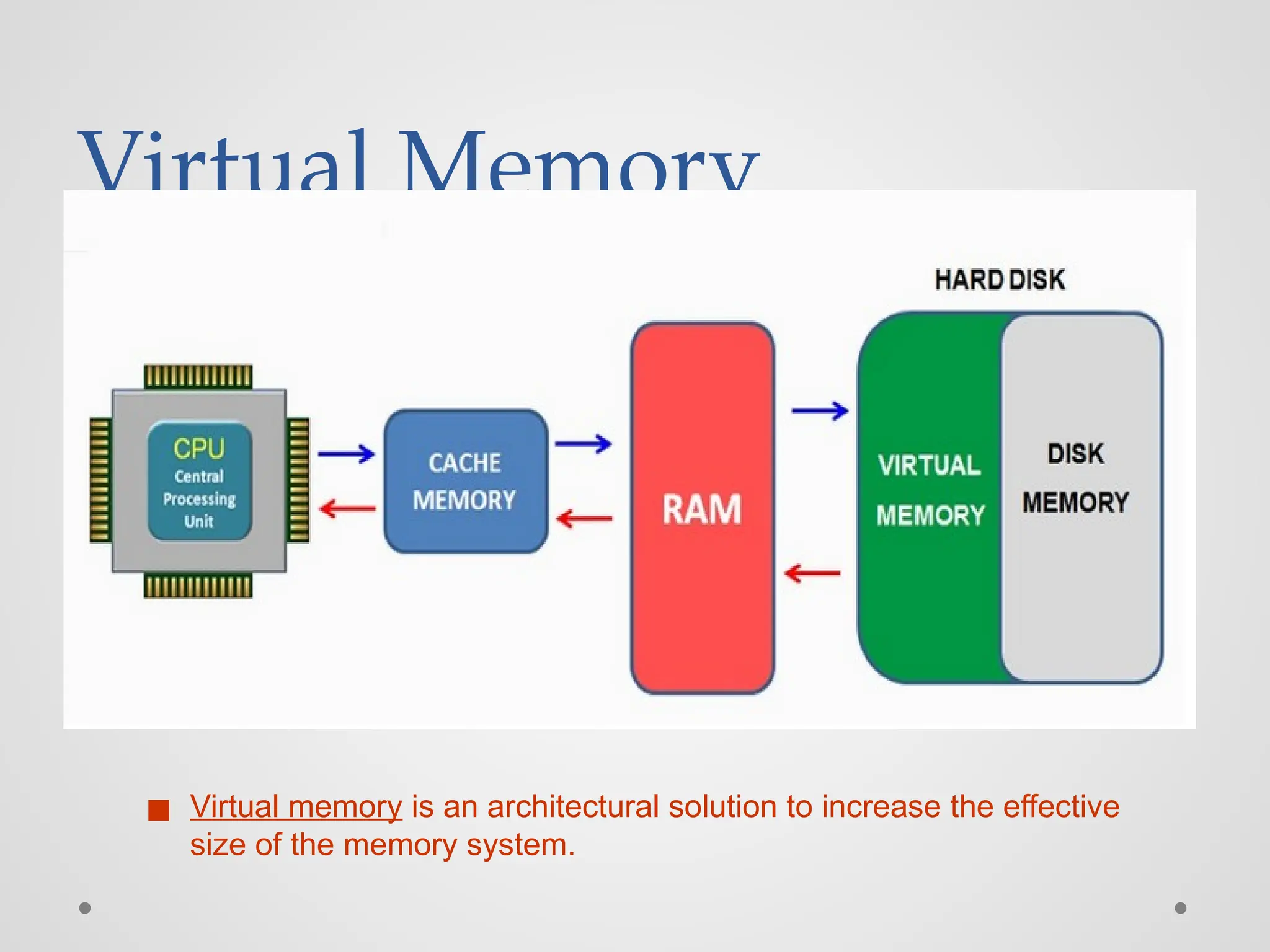
Virtual Memory ◼ Virtualmemory is an architectural solution to increase the effective size of the memory system.
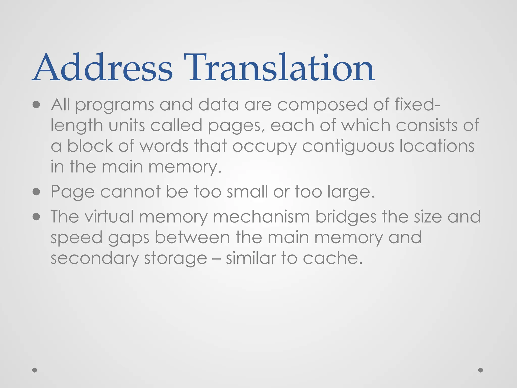
Address Translation ● Allprograms and data are composed of fixed- length units called pages, each of which consists of a block of words that occupy contiguous locations in the main memory. ● Page cannot be too small or too large. ● The virtual memory mechanism bridges the size and speed gaps between the main memory and secondary storage – similar to cache.
59.
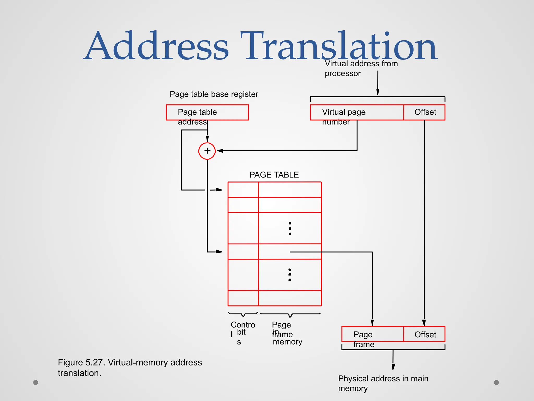
Address Translation Page frame Virtual addressfrom processor in memory Offset Offset Virtual page number Page table address Page table base register Figure 5.27. Virtual-memory address translation. Contro l bit s Physical address in main memory PAGE TABLE Page frame +
60.
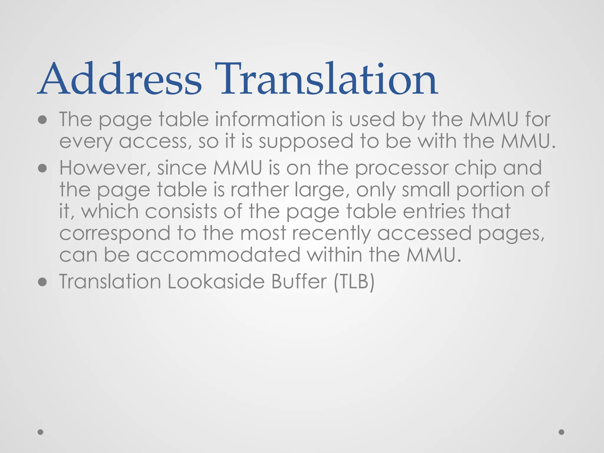
Address Translation ● Thepage table information is used by the MMU for every access, so it is supposed to be with the MMU. ● However, since MMU is on the processor chip and the page table is rather large, only small portion of it, which consists of the page table entries that correspond to the most recently accessed pages, can be accommodated within the MMU. ● Translation Lookaside Buffer (TLB)
61.
TLB Figure 5.28. Useof an associative-mapped TLB. No Yes Hit Miss Virtual address from processor TLB Offset Virtual page number number Virtual page Page frame in memory Control bits Offset Physical address in main memory Page frame =?
62.
Address translation (contd..) ◼What happens if a program generates an access to a page that is not in the main memory? ◼ In this case, a page fault is said to occur. ▪ Whole page must be brought into the main memory from the disk, before the execution can proceed. ◼ Upon detecting a page fault by the MMU, following actions occur: ▪ MMU asks the operating system to intervene by raising an exception. ▪ Processing of the active task which caused the page fault is interrupted. ▪ Control is transferred to the operating system. ▪ Operating system copies the requested page from secondary storage to the main memory. ▪ Once the page is copied, control is returned to the task which was interrupted. 62
63.
Address translation (contd..) ◼When a new page is to be brought into the main memory from secondary storage, the main memory may be full. ▪ Some page from the main memory must be replaced with this new page. ◼ How to choose which page to replace? ▪ This is similar to the replacement that occurs when the cache is full. ▪ The principle of locality of reference (?) can also be applied here. ▪ A replacement strategy similar to LRU can be applied. ◼ Since the size of the main memory is relatively larger compared to cache, a relatively large amount of programs and data can be held in the main memory. ▪ Minimizes the frequency of transfers between secondary storage and main memory. 63
64.
Cache & VirtualMemory ◼ Cache memory: ▪ Introduced to bridge the speed gap between the processor and the main memory. ▪ Implemented in hardware. ◼ Virtual memory: ▪ Introduced to bridge the speed gap between the main memory and secondary storage. ▪ Implemented in part by software. 64
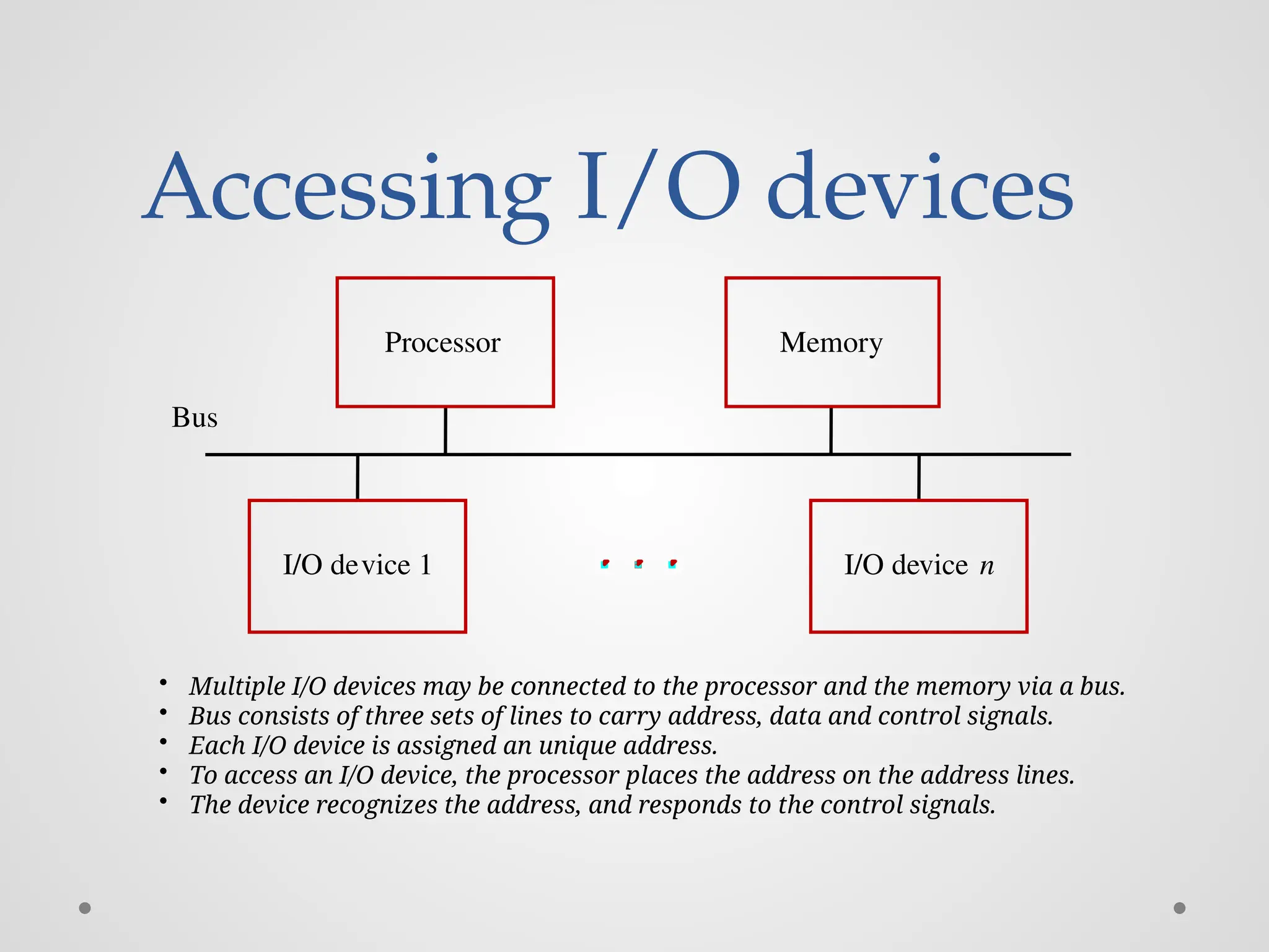
Accessing I/O devices Bus I/Odevice 1 I/O device n Processor Memory • Multiple I/O devices may be connected to the processor and the memory via a bus. • Bus consists of three sets of lines to carry address, data and control signals. • Each I/O device is assigned an unique address. • To access an I/O device, the processor places the address on the address lines. • The device recognizes the address, and responds to the control signals.
68.
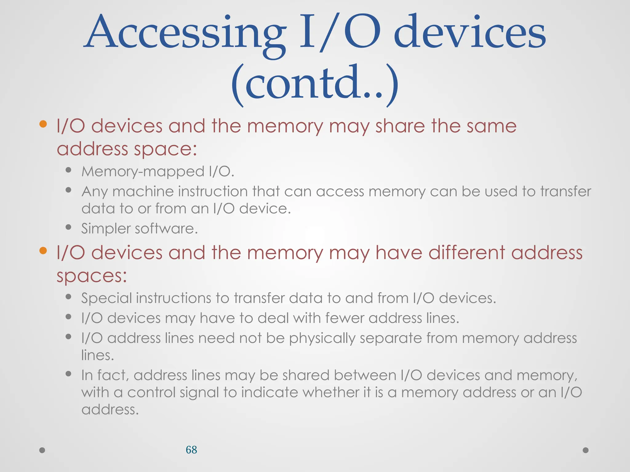
Accessing I/O devices (contd..) I/O devices and the memory may share the same address space: Memory-mapped I/O. Any machine instruction that can access memory can be used to transfer data to or from an I/O device. Simpler software. I/O devices and the memory may have different address spaces: Special instructions to transfer data to and from I/O devices. I/O devices may have to deal with fewer address lines. I/O address lines need not be physically separate from memory address lines. In fact, address lines may be shared between I/O devices and memory, with a control signal to indicate whether it is a memory address or an I/O address. 68
69.
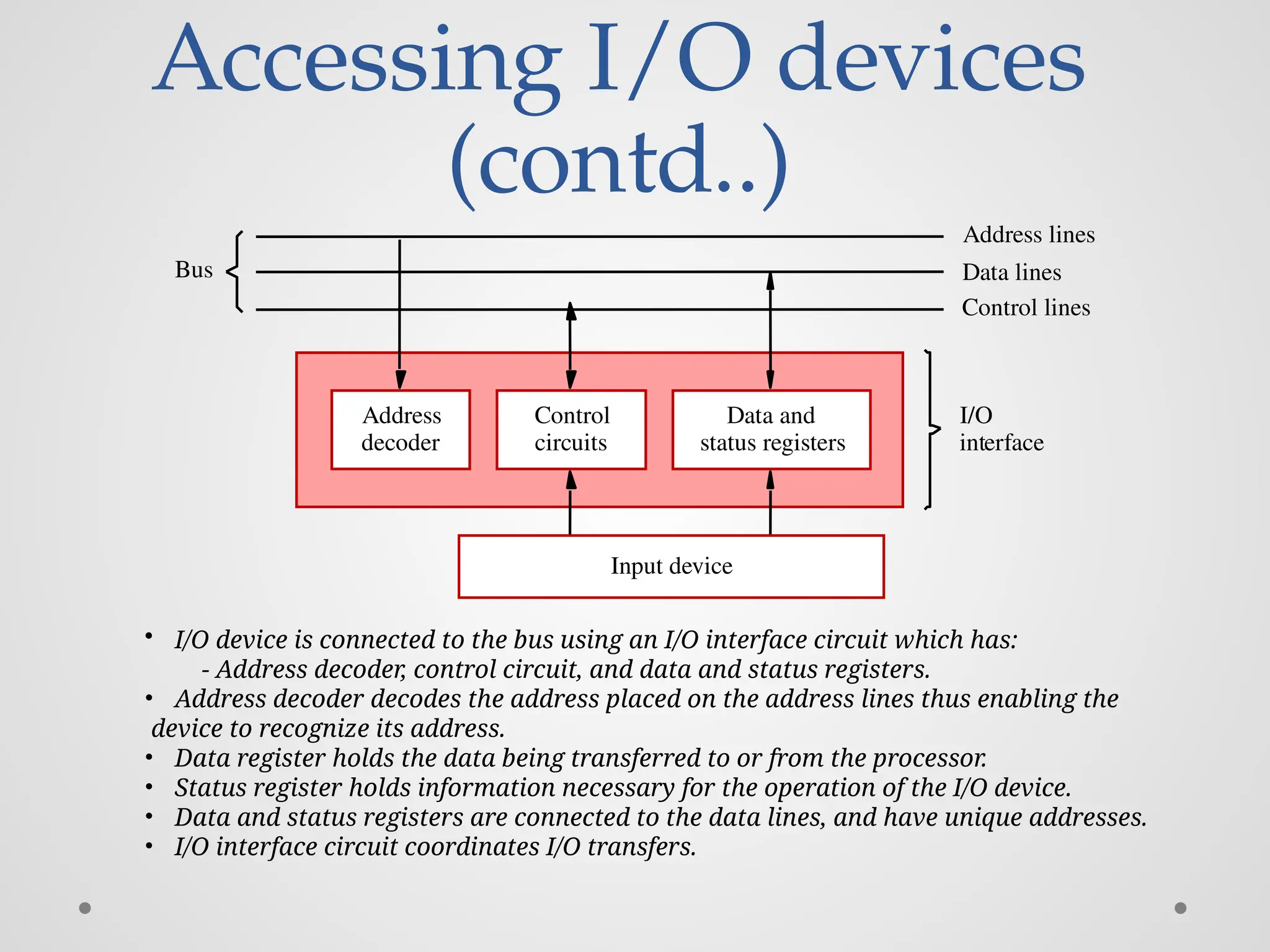
Accessing I/O devices (contd..) I/O interface decoder AddressData and status registers Control circuits Input device Bus Address lines Data lines Control lines • I/O device is connected to the bus using an I/O interface circuit which has: - Address decoder, control circuit, and data and status registers. • Address decoder decodes the address placed on the address lines thus enabling the device to recognize its address. • Data register holds the data being transferred to or from the processor. • Status register holds information necessary for the operation of the I/O device. • Data and status registers are connected to the data lines, and have unique addresses. • I/O interface circuit coordinates I/O transfers.
70.
Accessing I/O devices (contd..) Recall that the rate of transfer to and from I/O devices is slower than the speed of the processor. This creates the need for mechanisms to synchronize data transfers between them. Program-controlled I/O: Processor repeatedly monitors a status flag to achieve the necessary synchronization. Processor polls the I/O device. Two other mechanisms used for synchronizing data transfers between the processor and memory: Interrupts. Direct Memory Access.
Interrupts • In program-controlledI/O, when the processor continuously monitors the status of the device, it does not perform any useful tasks. • An alternate approach would be for the I/O device to alert the processor when it becomes ready. o Do so by sending a hardware signal called an interrupt to the processor. o At least one of the bus control lines, called an interrupt-request line is dedicated for this purpose. • Processor can perform other useful tasks while it is waiting for the device to be ready.
73.
Interrupt • An interruptis an event that causes the execution of one program to be suspended and execution of another program to be begin.
74.
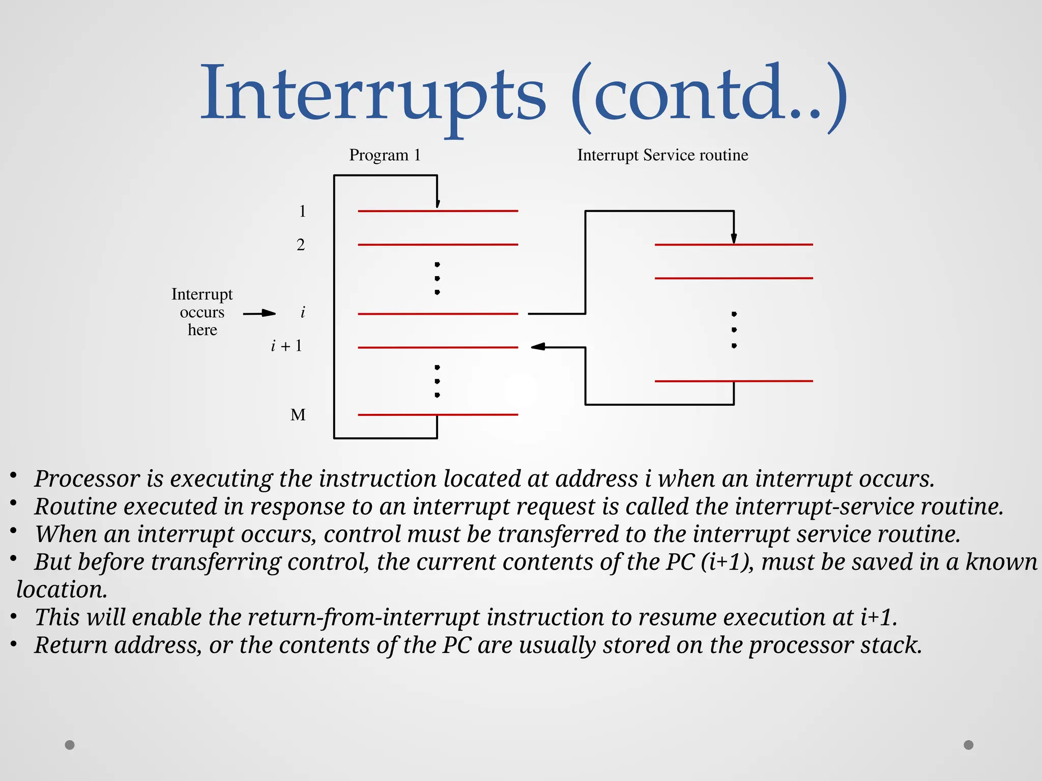
Interrupts (contd..) Interrupt Serviceroutine Program 1 here Interrupt occurs M i 2 1 i 1 + • Processor is executing the instruction located at address i when an interrupt occurs. • Routine executed in response to an interrupt request is called the interrupt-service routine. • When an interrupt occurs, control must be transferred to the interrupt service routine. • But before transferring control, the current contents of the PC (i+1), must be saved in a known location. • This will enable the return-from-interrupt instruction to resume execution at i+1. • Return address, or the contents of the PC are usually stored on the processor stack.
75.
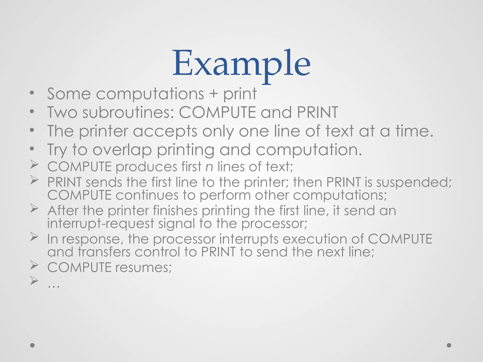
Example • Some computations+ print • Two subroutines: COMPUTE and PRINT • The printer accepts only one line of text at a time. • Try to overlap printing and computation. COMPUTE produces first n lines of text; PRINT sends the first line to the printer; then PRINT is suspended; COMPUTE continues to perform other computations; After the printer finishes printing the first line, it send an interrupt-request signal to the processor; In response, the processor interrupts execution of COMPUTE and transfers control to PRINT to send the next line; COMPUTE resumes; …
76.
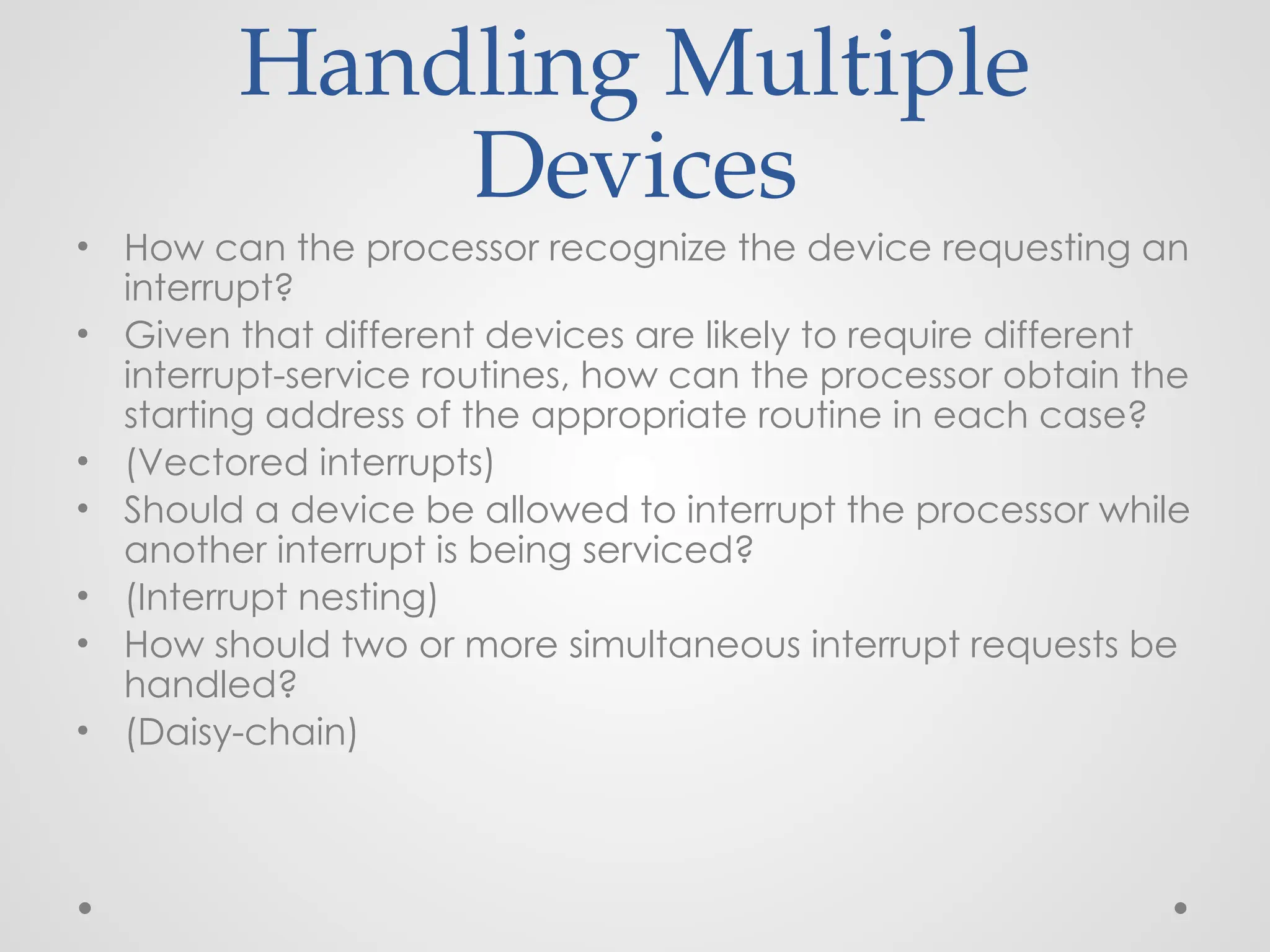
Handling Multiple Devices • Howcan the processor recognize the device requesting an interrupt? • Given that different devices are likely to require different interrupt-service routines, how can the processor obtain the starting address of the appropriate routine in each case? • (Vectored interrupts) • Should a device be allowed to interrupt the processor while another interrupt is being serviced? • (Interrupt nesting) • How should two or more simultaneous interrupt requests be handled? • (Daisy-chain)
77.
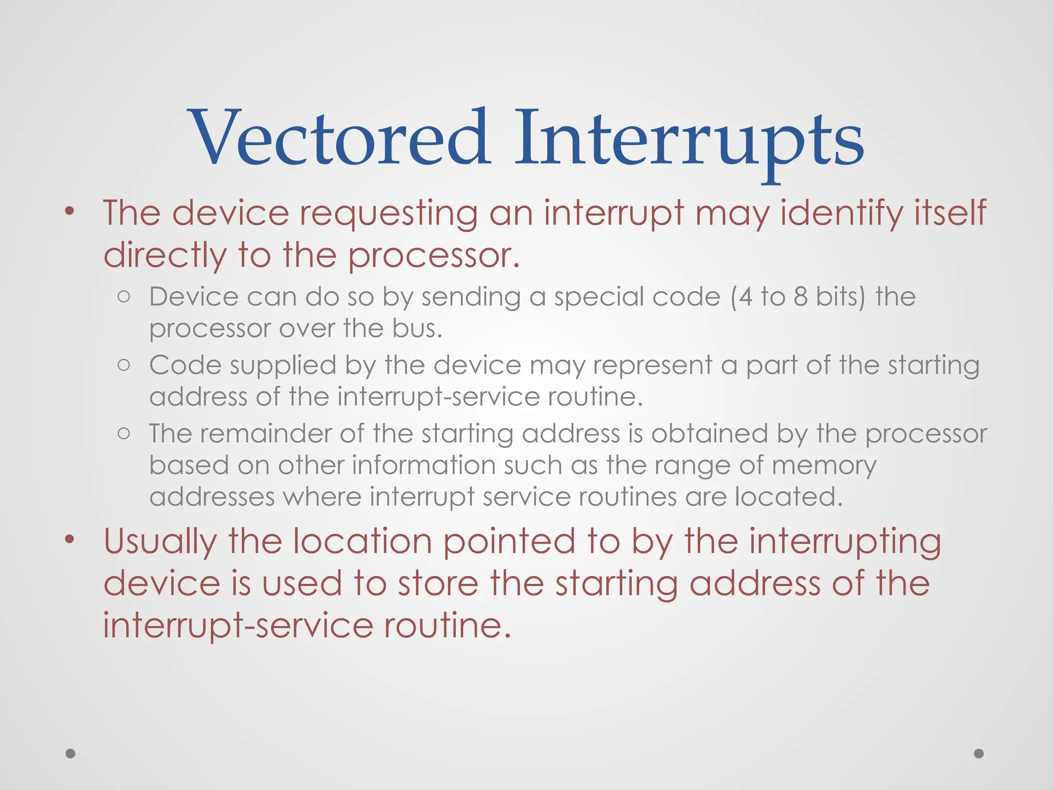
Vectored Interrupts • Thedevice requesting an interrupt may identify itself directly to the processor. o Device can do so by sending a special code (4 to 8 bits) the processor over the bus. o Code supplied by the device may represent a part of the starting address of the interrupt-service routine. o The remainder of the starting address is obtained by the processor based on other information such as the range of memory addresses where interrupt service routines are located. • Usually the location pointed to by the interrupting device is used to store the starting address of the interrupt-service routine.
78.
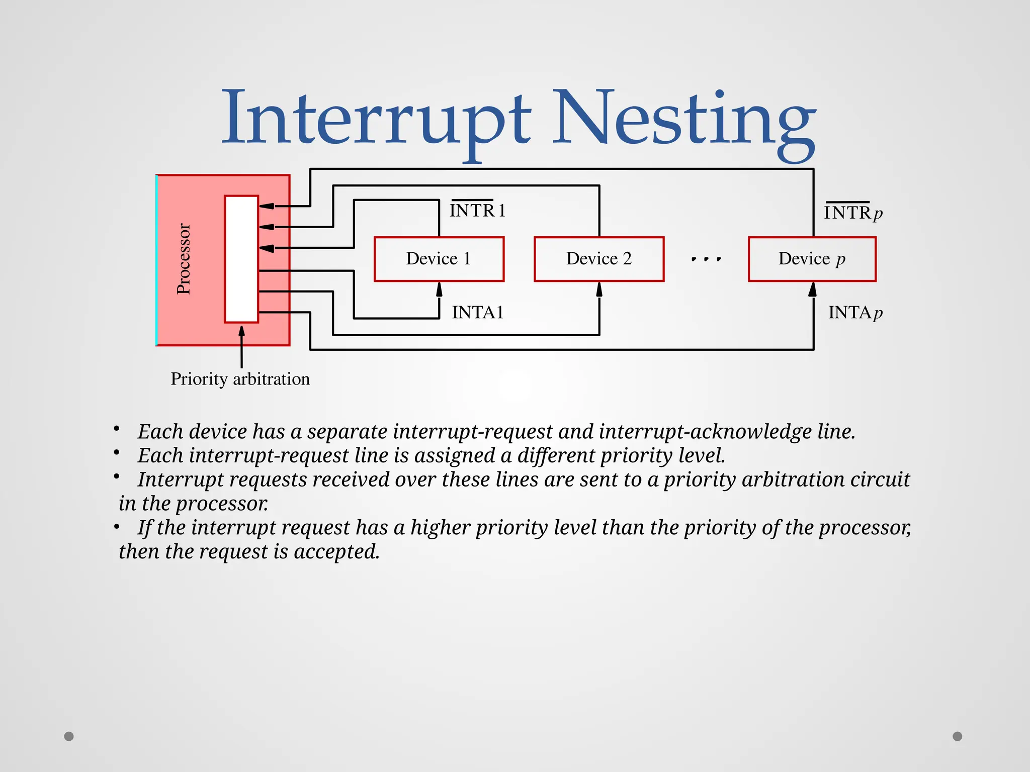
Interrupt Nesting Priority arbitration Device1 Device 2 Device p Processor INTA1 INTR1 INTRp INTAp • Each device has a separate interrupt-request and interrupt-acknowledge line. • Each interrupt-request line is assigned a different priority level. • Interrupt requests received over these lines are sent to a priority arbitration circuit in the processor. • If the interrupt request has a higher priority level than the priority of the processor, then the request is accepted.
79.
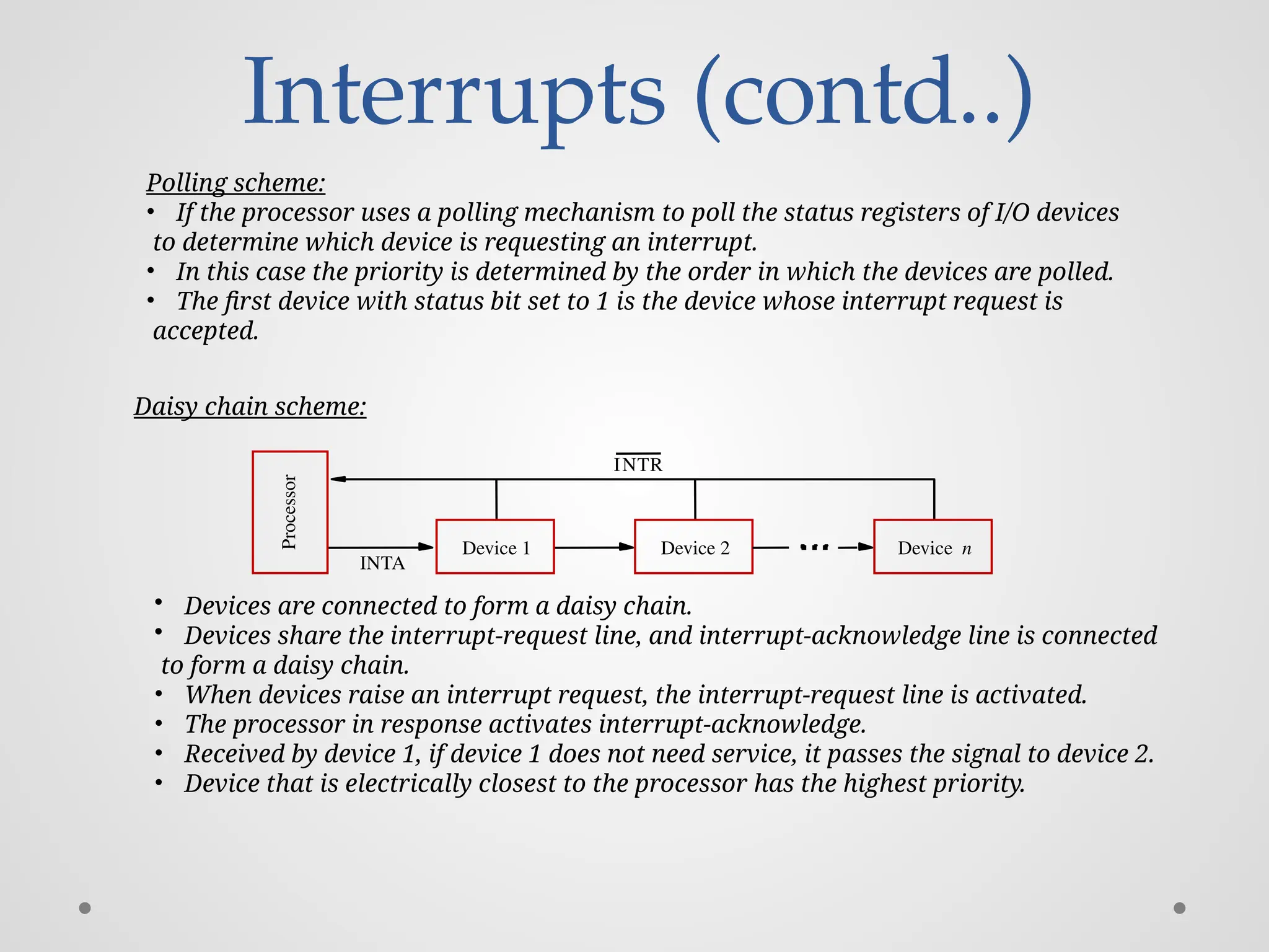
Interrupts (contd..) Processor Device 2 INTR INTA Devicen Device 1 Polling scheme: • If the processor uses a polling mechanism to poll the status registers of I/O devices to determine which device is requesting an interrupt. • In this case the priority is determined by the order in which the devices are polled. • The first device with status bit set to 1 is the device whose interrupt request is accepted. Daisy chain scheme: • Devices are connected to form a daisy chain. • Devices share the interrupt-request line, and interrupt-acknowledge line is connected to form a daisy chain. • When devices raise an interrupt request, the interrupt-request line is activated. • The processor in response activates interrupt-acknowledge. • Received by device 1, if device 1 does not need service, it passes the signal to device 2. • Device that is electrically closest to the processor has the highest priority.
80.
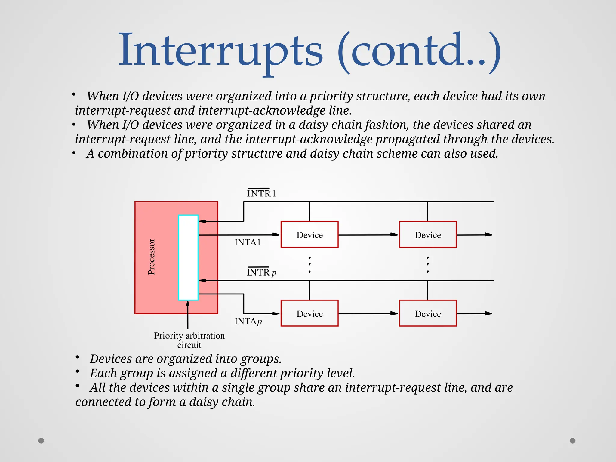
Interrupts (contd..) • WhenI/O devices were organized into a priority structure, each device had its own interrupt-request and interrupt-acknowledge line. • When I/O devices were organized in a daisy chain fashion, the devices shared an interrupt-request line, and the interrupt-acknowledge propagated through the devices. • A combination of priority structure and daisy chain scheme can also used. Device Device circuit Priority arbitration Processor Device Device INTR1 INTR p INTA1 INTAp • Devices are organized into groups. • Each group is assigned a different priority level. • All the devices within a single group share an interrupt-request line, and are connected to form a daisy chain.
81.
Exceptions Interrupts causedby interrupt-requests sent by I/O devices. Interrupts could be used in many other situations where the execution of one program needs to be suspended and execution of another program needs to be started. In general, the term exception is used to refer to any event that causes an interruption. Interrupt-requests from I/O devices is one type of an exception. Other types of exceptions are: Recovery from errors Debugging Privilege exception
Direct Memory Access (contd..) Direct Memory Access (DMA): A special control unit may be provided to transfer a block of data directly between an I/O device and the main memory, without continuous intervention by the processor. Control unit which performs these transfers is a part of the I/O device’s interface circuit. This control unit is called as a DMA controller. DMA controller performs functions that would be normally carried out by the processor: For each word, it provides the memory address and all the control signals. To transfer a block of data, it increments the memory addresses and keeps track of the number of transfers.
84.
Direct Memory Access (contd..) DMA controller can transfer a block of data from an external device to the processor, without any intervention from the processor. However, the operation of the DMA controller must be under the control of a program executed by the processor. That is, the processor must initiate the DMA transfer. To initiate the DMA transfer, the processor informs the DMA controller of: Starting address, Number of words in the block. Direction of transfer (I/O device to the memory, or memory to the I/O device). Once the DMA controller completes the DMA transfer, it informs the processor by raising an interrupt signal.
85.
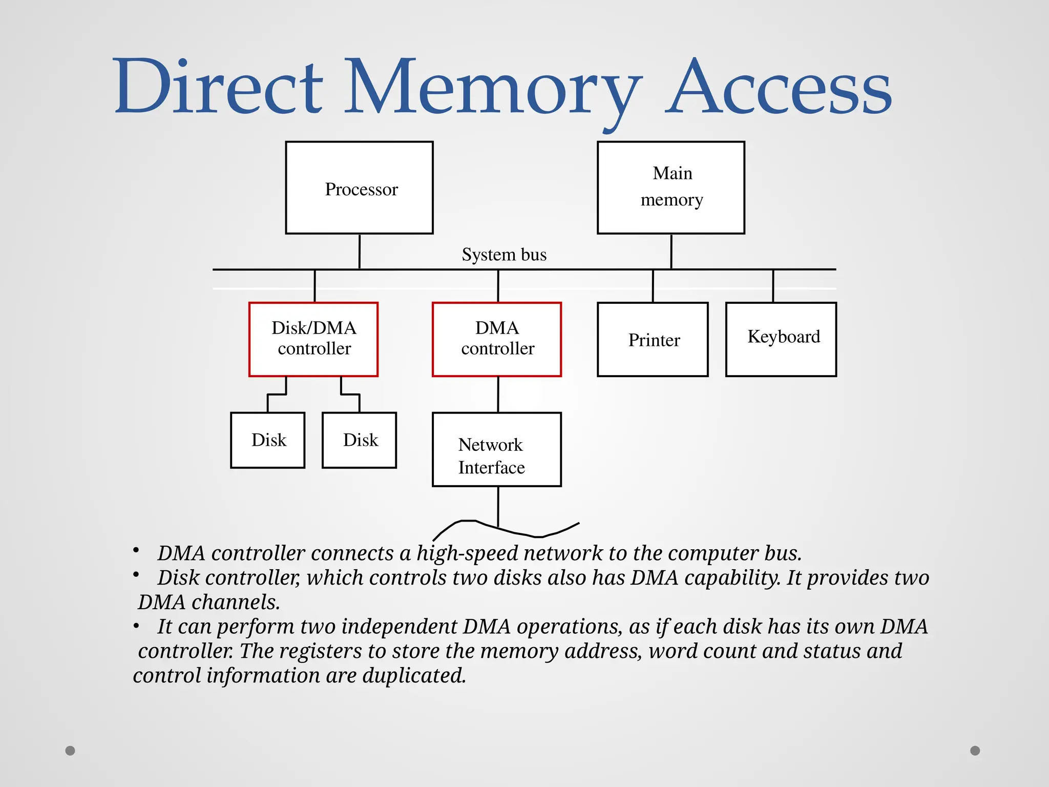
Direct Memory Access memory Processor Systembus Main Keyboard Disk/DMA controller Printer DMA controller Disk Disk • DMA controller connects a high-speed network to the computer bus. • Disk controller, which controls two disks also has DMA capability. It provides two DMA channels. • It can perform two independent DMA operations, as if each disk has its own DMA controller. The registers to store the memory address, word count and status and control information are duplicated. Network Interface
86.
Direct Memory Access (contd..) Processor and DMA controllers have to use the bus in an interwoven fashion to access the memory. DMA devices are given higher priority than the processor to access the bus. Among different DMA devices, high priority is given to high-speed peripherals such as a disk or a graphics display device. Processor originates most memory access cycles on the bus. DMA controller can be said to “steal” memory access cycles from the bus. This interweaving technique is called as “cycle stealing”. An alternate approach is the provide a DMA controller an exclusive capability to initiate transfers on the bus, and hence exclusive access to the main memory. This is known as the block or burst mode.
87.
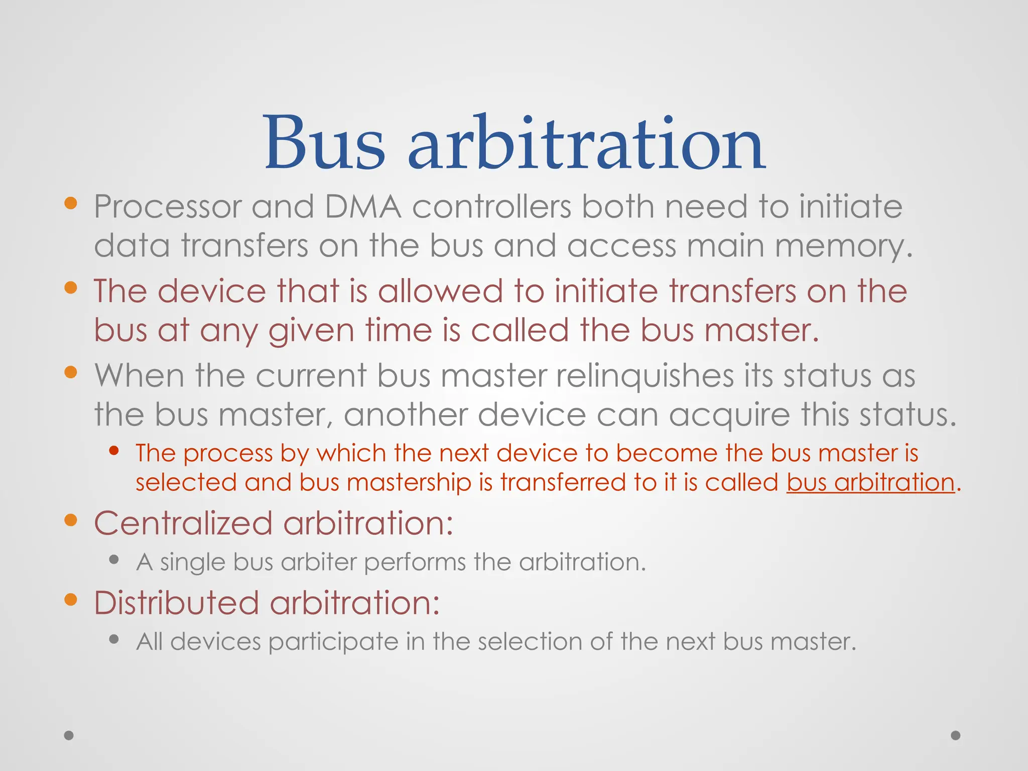
Bus arbitration Processorand DMA controllers both need to initiate data transfers on the bus and access main memory. The device that is allowed to initiate transfers on the bus at any given time is called the bus master. When the current bus master relinquishes its status as the bus master, another device can acquire this status. The process by which the next device to become the bus master is selected and bus mastership is transferred to it is called bus arbitration. Centralized arbitration: A single bus arbiter performs the arbitration. Distributed arbitration: All devices participate in the selection of the next bus master.
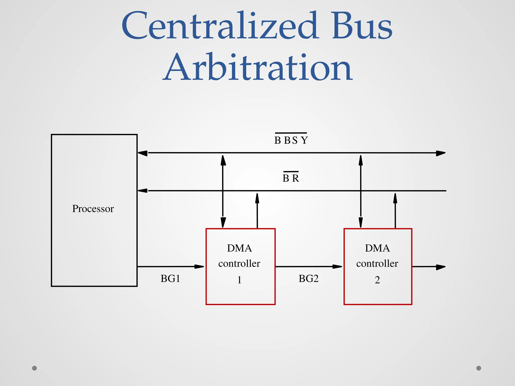
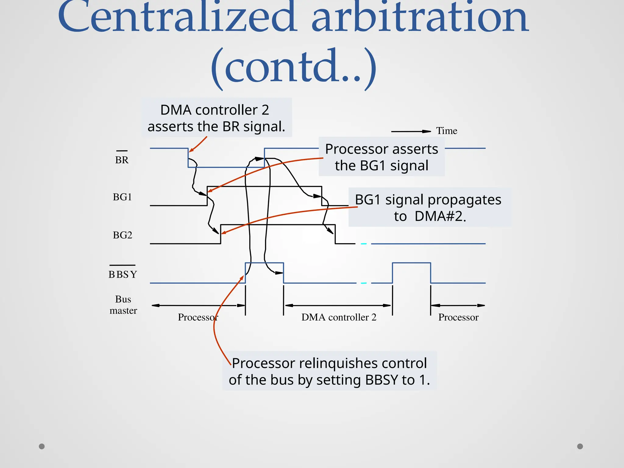
Centralized Bus Arbitration(cont.,) • Busarbiter may be the processor or a separate unit connected to the bus. • Normally, the processor is the bus master, unless it grants bus membership to one of the DMA controllers. • DMA controller requests the control of the bus by asserting the Bus Request (BR) line. • In response, the processor activates the Bus-Grant1 (BG1) line, indicating that the controller may use the bus when it is free. • BG1 signal is connected to all DMA controllers in a daisy chain fashion. • BBSY signal is 0, it indicates that the bus is busy. When BBSY becomes 1, the DMA controller which asserted BR can acquire control of the bus.
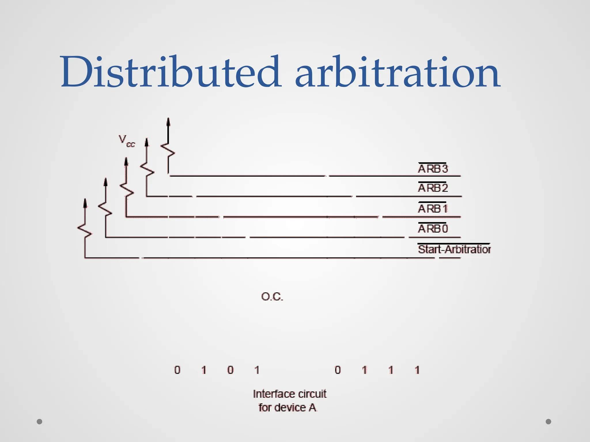
Distributed arbitration Alldevices waiting to use the bus share the responsibility of carrying out the arbitration process. Arbitration process does not depend on a central arbiter and hence distributed arbitration has higher reliability. Each device is assigned a 4-bit ID number. All the devices are connected using 5 lines, 4 arbitration lines to transmit the ID, and one line for the Start-Arbitration signal. To request the bus a device: Asserts the Start-Arbitration signal. Places its 4-bit ID number on the arbitration lines. The pattern that appears on the arbitration lines is the logical-OR of all the 4-bit device IDs placed on the arbitration lines.
Distributed arbitration(Contd.,) • Arbitration process: oEach device compares the pattern that appears on the arbitration lines to its own ID, starting with MSB. o If it detects a difference, it transmits 0s on the arbitration lines for that and all lower bit positions. o The pattern that appears on the arbitration lines is the logical-OR of all the 4-bit device IDs placed on the arbitration lines.
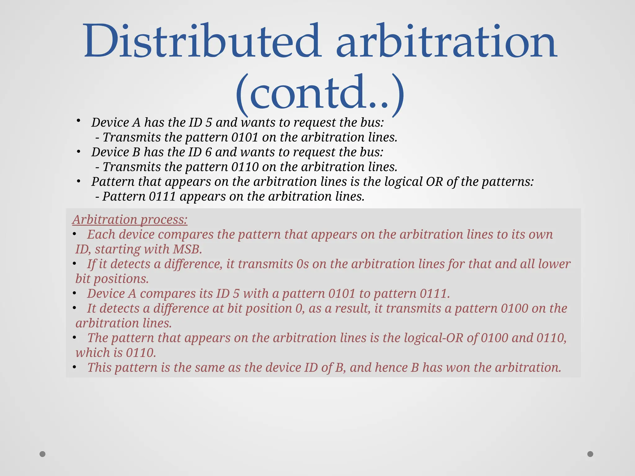
94.
Distributed arbitration (contd..) • DeviceA has the ID 5 and wants to request the bus: - Transmits the pattern 0101 on the arbitration lines. • Device B has the ID 6 and wants to request the bus: - Transmits the pattern 0110 on the arbitration lines. • Pattern that appears on the arbitration lines is the logical OR of the patterns: - Pattern 0111 appears on the arbitration lines. Arbitration process: • Each device compares the pattern that appears on the arbitration lines to its own ID, starting with MSB. • If it detects a difference, it transmits 0s on the arbitration lines for that and all lower bit positions. • Device A compares its ID 5 with a pattern 0101 to pattern 0111. • It detects a difference at bit position 0, as a result, it transmits a pattern 0100 on the arbitration lines. • The pattern that appears on the arbitration lines is the logical-OR of 0100 and 0110, which is 0110. • This pattern is the same as the device ID of B, and hence B has won the arbitration.
Buses • Processor, mainmemory, and I/O devices are interconnected by means of a bus. • Bus provides a communication path for the transfer of data. o Bus also includes lines to support interrupts and arbitration. • A bus protocol is the set of rules that govern the behavior of various devices connected to the bus, as to when to place information on the bus, when to assert control signals, etc.
97.
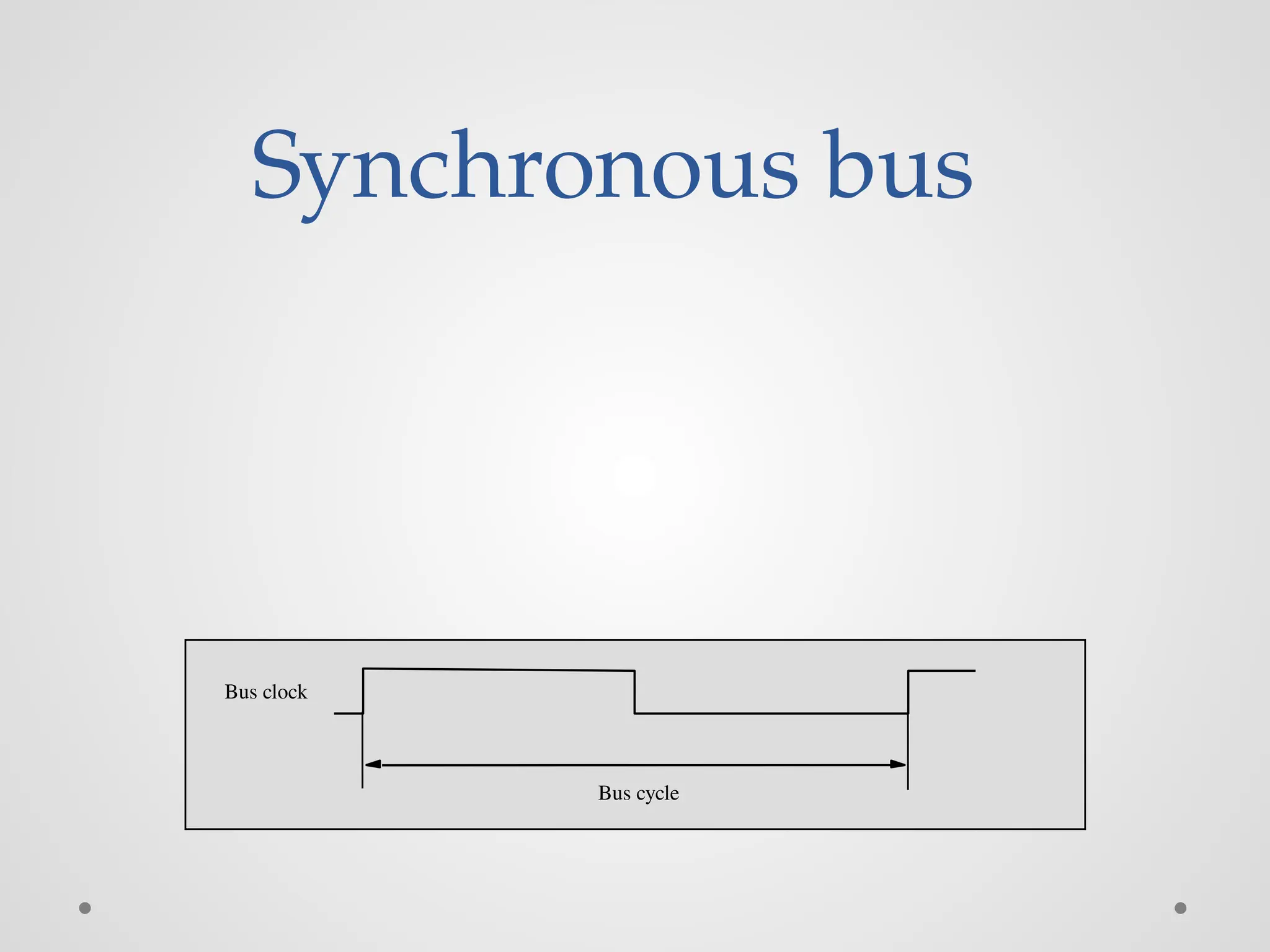
Buses (contd..) Buslines may be grouped into three types: Data Address Control Control signals specify: Whether it is a read or a write operation. Required size of the data, when several operand sizes (byte, word, long word) are possible. Timing information to indicate when the processor and I/O devices may place data or receive data from the bus. Schemes for timing of data transfers over a bus can be classified into: Synchronous, Asynchronous.
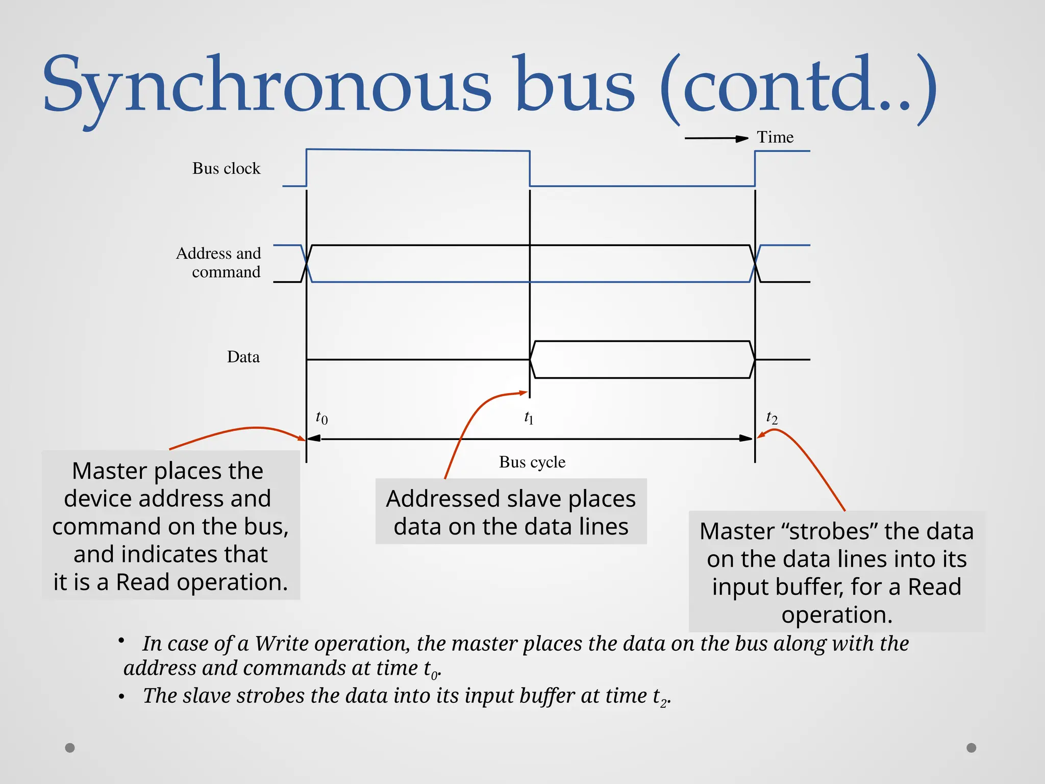
Synchronous bus (contd..) Buscycle Data Bus clock command Address and t0 t1 t2 Time Master places the device address and command on the bus, and indicates that it is a Read operation. Addressed slave places data on the data lines Master “strobes” the data on the data lines into its input buffer, for a Read operation. • In case of a Write operation, the master places the data on the bus along with the address and commands at time t0. • The slave strobes the data into its input buffer at time t2.
100.
Synchronous bus (contd..) •Once the master places the device address and command on the bus, it takes time for this information to propagate to the devices: o This time depends on the physical and electrical characteristics of the bus. • Also, all the devices have to be given enough time to decode the address and control signals, so that the addressed slave can place data on the bus. • Width of the pulse t1 - t0 depends on: o Maximum propagation delay between two devices connected to the bus. o Time taken by all the devices to decode the address and control signals, so that the addressed slave can respond at time t1.
101.
Synchronous bus (contd..) •At the end of the clock cycle, at time t2, the master strobes the data on the data lines into its input buffer if it’s a Read operation. o “Strobe” means to capture the values of the data and store them into a buffer. • When data are to be loaded into a storage buffer register, the data should be available for a period longer than the setup time of the device. • Width of the pulse t2 - t1 should be longer than: o Maximum propagation time of the bus plus o Set up time of the input buffer register of the master.
102.
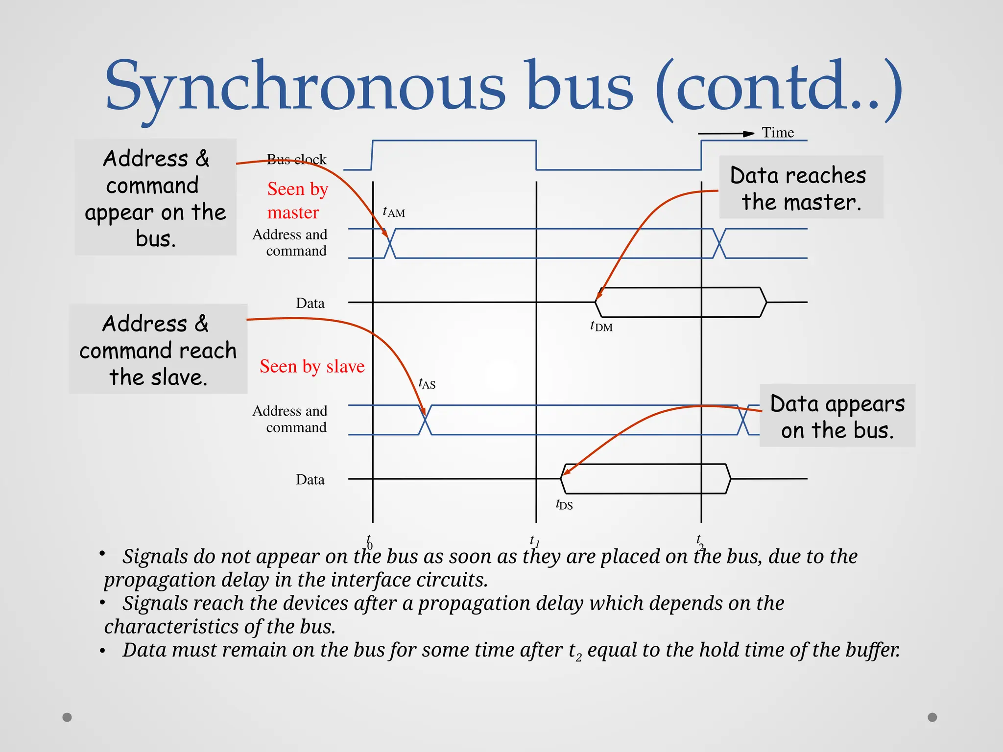
Synchronous bus (contd..) Data Busclock command Address and t 0 t1 t 2 command Address and Data Seen by master Seen by slave tAM tAS tDS tDM Time • Signals do not appear on the bus as soon as they are placed on the bus, due to the propagation delay in the interface circuits. • Signals reach the devices after a propagation delay which depends on the characteristics of the bus. • Data must remain on the bus for some time after t2 equal to the hold time of the buffer. Address & command appear on the bus. Address & command reach the slave. Data appears on the bus. Data reaches the master.
103.
Synchronous bus (contd..) •Data transfer has to be completed within one clock cycle. o Clock period t2 - t0 must be such that the longest propagation delay on the bus and the slowest device interface must be accommodated. o Forces all the devices to operate at the speed of the slowest device. • Processor just assumes that the data are available at t2 in case of a Read operation, or are read by the device in case of a Write operation. o What if the device is actually failed, and never really responded?
104.
Synchronous bus (contd..) •Most buses have control signals to represent a response from the slave. • Control signals serve two purposes: o Inform the master that the slave has recognized the address, and is ready to participate in a data transfer operation. o Enable to adjust the duration of the data transfer operation based on the speed of the participating slaves. • High-frequency bus clock is used: o Data transfer spans several clock cycles instead of just one clock cycle as in the earlier case.
105.
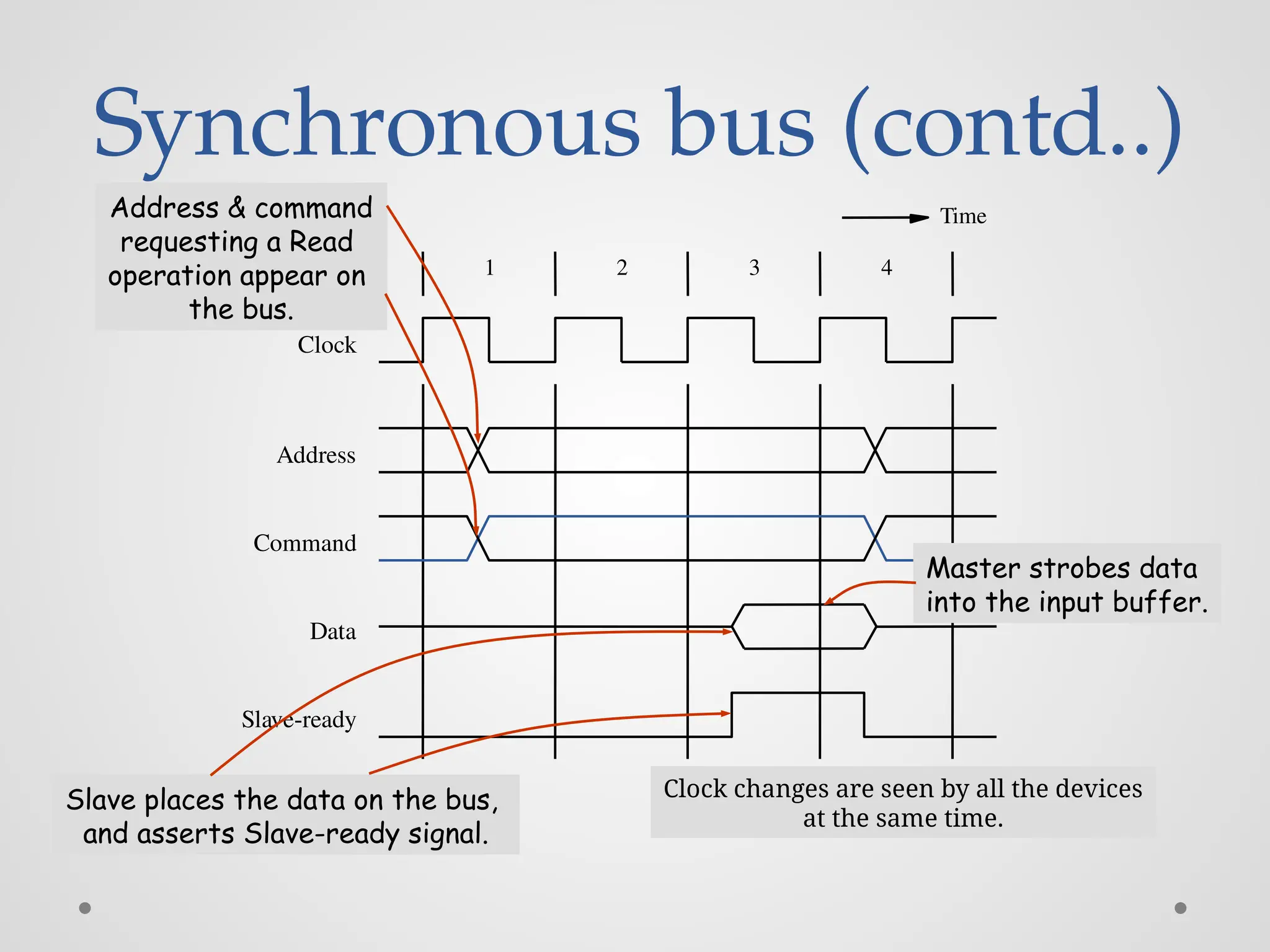
Synchronous bus (contd..) 12 3 4 Clock Address Command Data Slave-ready Time Address & command requesting a Read operation appear on the bus. Slave places the data on the bus, and asserts Slave-ready signal. Master strobes data into the input buffer. Clock changes are seen by all the devices at the same time.
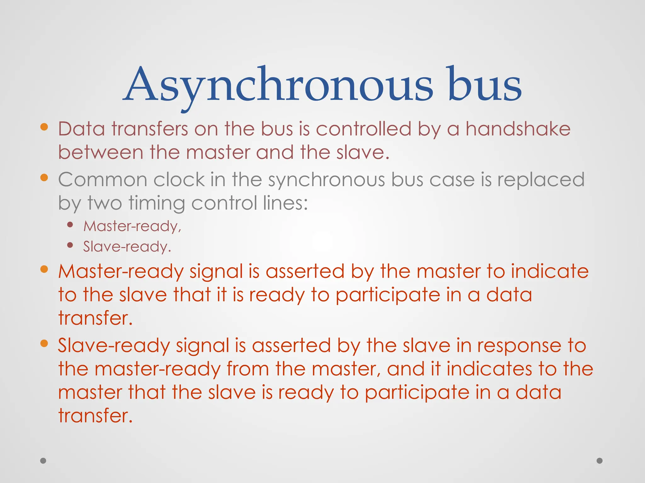
106.
Asynchronous bus Datatransfers on the bus is controlled by a handshake between the master and the slave. Common clock in the synchronous bus case is replaced by two timing control lines: Master-ready, Slave-ready. Master-ready signal is asserted by the master to indicate to the slave that it is ready to participate in a data transfer. Slave-ready signal is asserted by the slave in response to the master-ready from the master, and it indicates to the master that the slave is ready to participate in a data transfer.
107.
Asynchronous bus (contd..) • Datatransfer using the handshake protocol: o Master places the address and command information on the bus. o Asserts the Master-ready signal to indicate to the slaves that the address and command information has been placed on the bus. o All devices on the bus decode the address. o Address slave performs the required operation, and informs the processor it has done so by asserting the Slave-ready signal. o Master removes all the signals from the bus, once Slave-ready is asserted. o If the operation is a Read operation, Master also strobes the data into its input buffer.
108.
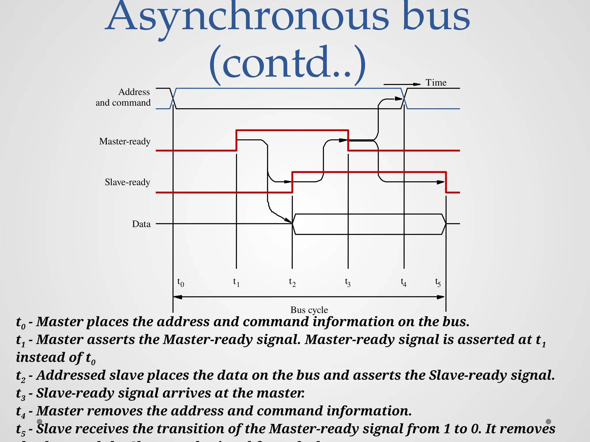
Asynchronous bus (contd..) Slave-ready Data Master-ready and command Address Buscycle t1 t2 t3 t4 t5 t0 Time t0 - Master places the address and command information on the bus. t1 - Master asserts the Master-ready signal. Master-ready signal is asserted at t1 instead of t0 t2 - Addressed slave places the data on the bus and asserts the Slave-ready signal. t3 - Slave-ready signal arrives at the master . t4 - Master removes the address and command information. t5 - Slave receives the transition of the Master-ready signal from 1 to 0. It removes
109.
Asynchronous vs. Synchronous bus •Advantages of asynchronous bus: o Eliminates the need for synchronization between the sender and the receiver. o Can accommodate varying delays automatically, using the Slave-ready signal. • Disadvantages of asynchronous bus: o Data transfer rate with full handshake is limited by two-round trip delays. o Data transfers using a synchronous bus involves only one round trip delay, and hence a synchronous bus can achieve faster rates.
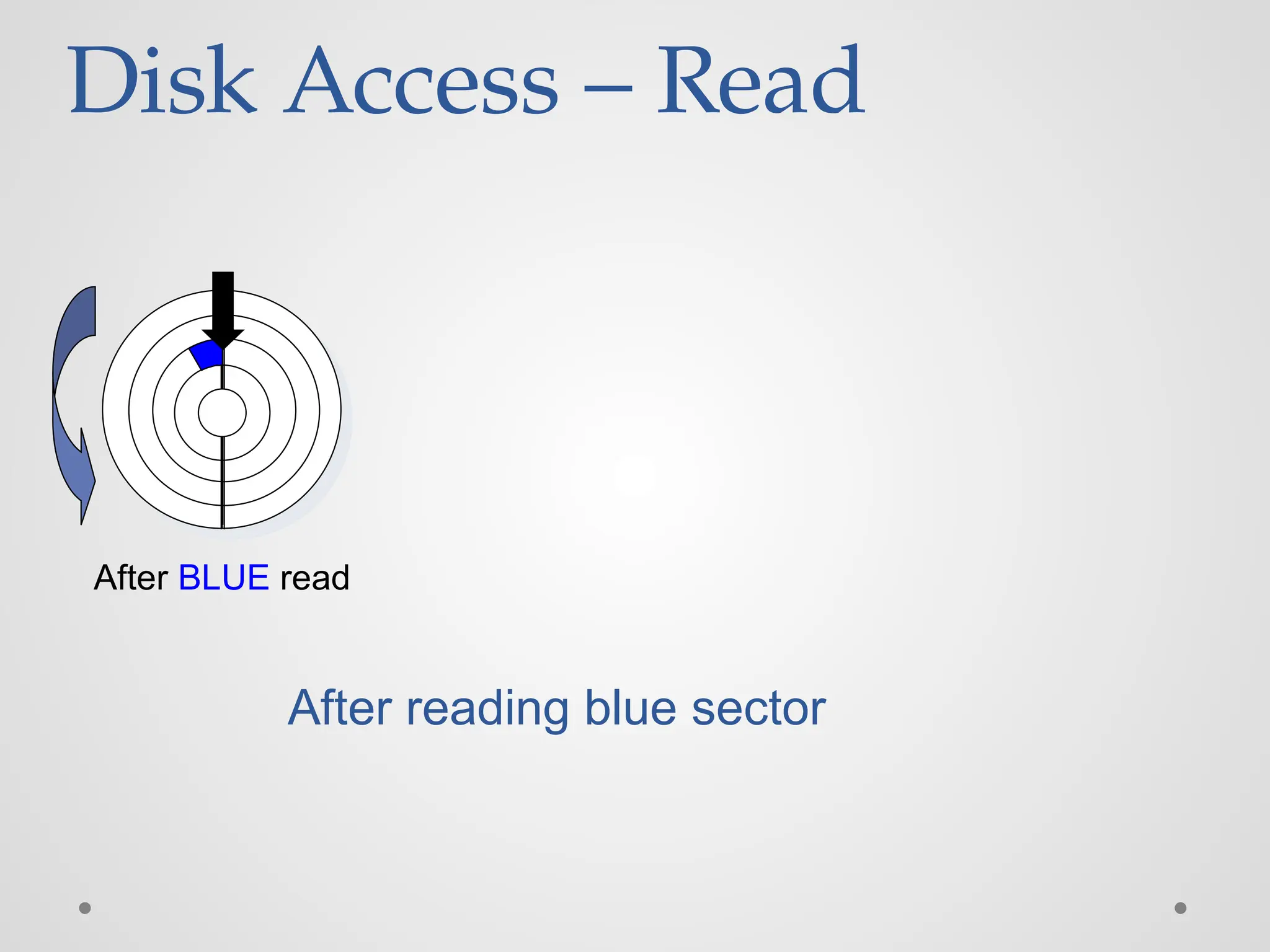
#27 Goal: Show the inefficeincy of current disk requests. Conveyed Ideas: Rotational latency is wasted time that can be used to service tasks Background Information: None. Slide Background: None. Kill text and arrows
#28 Goal: Show the inefficeincy of current disk requests. Conveyed Ideas: Rotational latency is wasted time that can be used to service tasks Background Information: None. Slide Background: None. Kill text and arrows
#29 Goal: Show the inefficeincy of current disk requests. Conveyed Ideas: Rotational latency is wasted time that can be used to service tasks Background Information: None. Slide Background: None. Kill text and arrows
#30 Goal: Show the inefficeincy of current disk requests. Conveyed Ideas: Rotational latency is wasted time that can be used to service tasks Background Information: None. Slide Background: None. Kill text and arrows
#31 Goal: Show the inefficeincy of current disk requests. Conveyed Ideas: Rotational latency is wasted time that can be used to service tasks Background Information: None. Slide Background: None. Kill text and arrows
#32 Goal: Show the inefficeincy of current disk requests. Conveyed Ideas: Rotational latency is wasted time that can be used to service tasks Background Information: None. Slide Background: None. Kill text and arrows
#33 Goal: Show the inefficeincy of current disk requests. Conveyed Ideas: Rotational latency is wasted time that can be used to service tasks Background Information: None. Slide Background: None. Kill text and arrows
#34 Goal: Show the inefficeincy of current disk requests. Conveyed Ideas: Rotational latency is wasted time that can be used to service tasks Background Information: None. Slide Background: None. Kill text and arrows
#35 Goal: Show the inefficeincy of current disk requests. Conveyed Ideas: Rotational latency is wasted time that can be used to service tasks Background Information: None. Slide Background: None. Kill text and arrows
#36 Goal: Show the inefficeincy of current disk requests. Conveyed Ideas: Rotational latency is wasted time that can be used to service tasks Background Information: None. Slide Background: None. Kill text and arrows
#83 This alternative approach is called as direct memory access. DMA consists of a special control unit which is provided to transfer a block of data directly between an I/O device and the main memory without continuous intervention by the processor. A control unit which performs these transfers without the intervention of the processor is a part of the I/O device’s interface circuit, and this controller is called as the DMA controller. DMA controller performs functions that would be normally be performed by the processor. The processor will have to provide a memory address and all the control signals. So, the DMA controller will also provide with the memory address where the data is going to be stored along with the necessary control signals. When a block of data needs to be transferred, the DMA controller will also have to increment the memory addresses and keep track of the number of words that have been transferred.
#84 Repeat DMA controller. DMA controller can be used to transfer a block of data from an external device to the processor, without requiring any help from the processor. As a result the processor is free to execute other programs. However, the DMA controller should perform the task of transferring data to or from an I/O device for a program that is being executed by a processor. That is, the DMA controller does not and should not have the capability to determine when a data transfer operation should take place. The processor must initiate DMA transfer of data, when it is indicated or required by the program that is being executed by the processor. When the processor determines that the program that is being executed requires a DMA transfer, it informs the DMA controller which sits in the interface circuit of the device of three things, namely, the starting address of the memory location, the number of words that needs to be transferred, and the direction of transfer that is, whether the data needs to be transferred from the I/O device to the memory or from the memory to the I/O device. After initiating the DMA transfer, the processor suspends the program that initiated the transfer, and continues with the execution of some other program. The program whose execution is suspended is said to be in the blocked state.
#85 Let us consider a memory organization with two DMA controllers. In this memory organization, a DMA controller is used to connect a high speed network to the computer bus. In addition, disk controller which also controls two disks may have DMA capability. The disk controller controls two disks and it also has DMA capability. The disk controller provides two DMA channels. The disk controller can two independent DMA operations, as if each disk has its own DMA controller. Each DMA controller has three registers, one to store the memory address, one to store the word count, and the last to store the status and control information. There are two copies of these three registers in order to perform independent DMA operations. That is, these registers are duplicated.
#86 Processor also has to transfer data to and from the main memory. Also, the DMA controller is responsible for transferring data to and from the I/O device to the main memory. Both the processor and the DMA controller have to use the external bus to talk to the main memory. Usually, DMA controllers are given higher priority than the processor to access the bus. Now, we also need to decide the priority among different DMA devices that may need to use the bus. Among these different DMA devices, high priority is given to high speed peripherals such as a disk or a graphics display device. Usually, the processor originates most cycles on the bus. The DMA controller can be said to steal memory access cycles on from the bus. Thus, the processor and the DMA controller use the bus in an interwoven fashion. This interweaving technique is called as cycle stealing. An alternate approach would be to provide DMA controllers exclusive capability to initiate transfers on the bus, and hence exclusive access to the main memory. This is known as the block mode or the burst mode of operation.
#87 Processor and DMA controllers both need to initiate data transfers on the bus and access main memory. The process of using the bus to perform a data transfer operation is called as the initiation of a transfer operation. At any point in time only one device is allowed to initiate transfers on the bus. The device that is allowed to initiate transfers on the bus at any given time is called the bus master. When the current bus master releases control of the bus, another device can acquire the status of the bus master. How does one determine which is the next device which will acquire the status of the bus master. Note that there may be several DMA controllers plus the processor which requires access to the bus. The process by which the next device to become the bus master is selected and bus mastership is transferred to it is called bus arbitration. There are two types of bus arbitration processes. Centralized arbitration and distributed arbitration. In case of centralized arbitration, a single bus arbiter performs the arbitration. Whereas in case of distributed arbitration all devices which need to initiate data transfers on the bus participate or are involved in the selection of the next bus master.
#97 Recall that one device plays the role of a master. The device that initiates the data transfer on the bus by issuing read or write control signals is called as a master. The device that is being addressed by the master is called a slave or a target.
#105 Slave-ready signal is an acknowledgement from the slave to the master to confirm that the valid data has been sent. Depending on when the slave-ready signal is asserted, the duration of the data transfer can change.