Download as PDF, PPTX

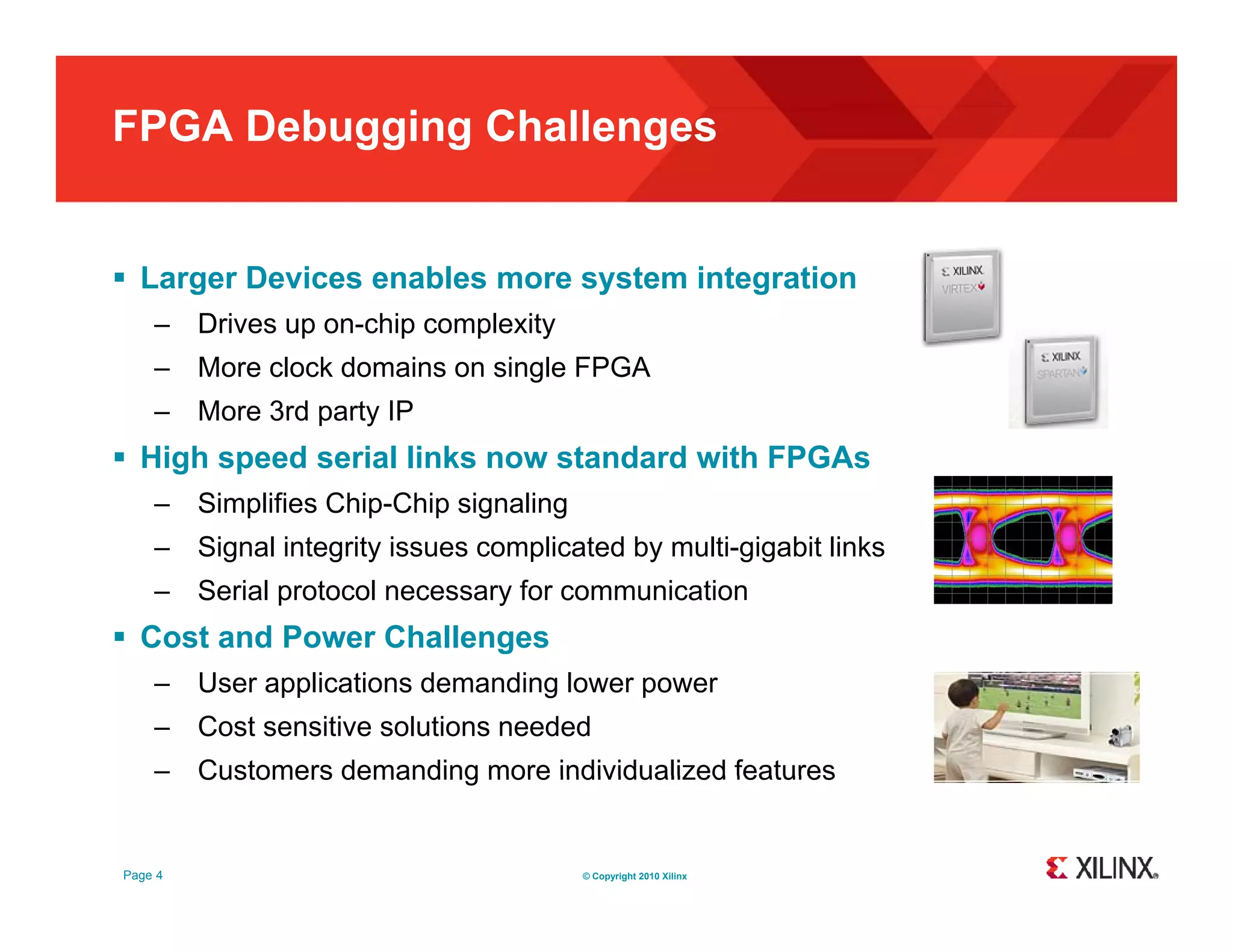
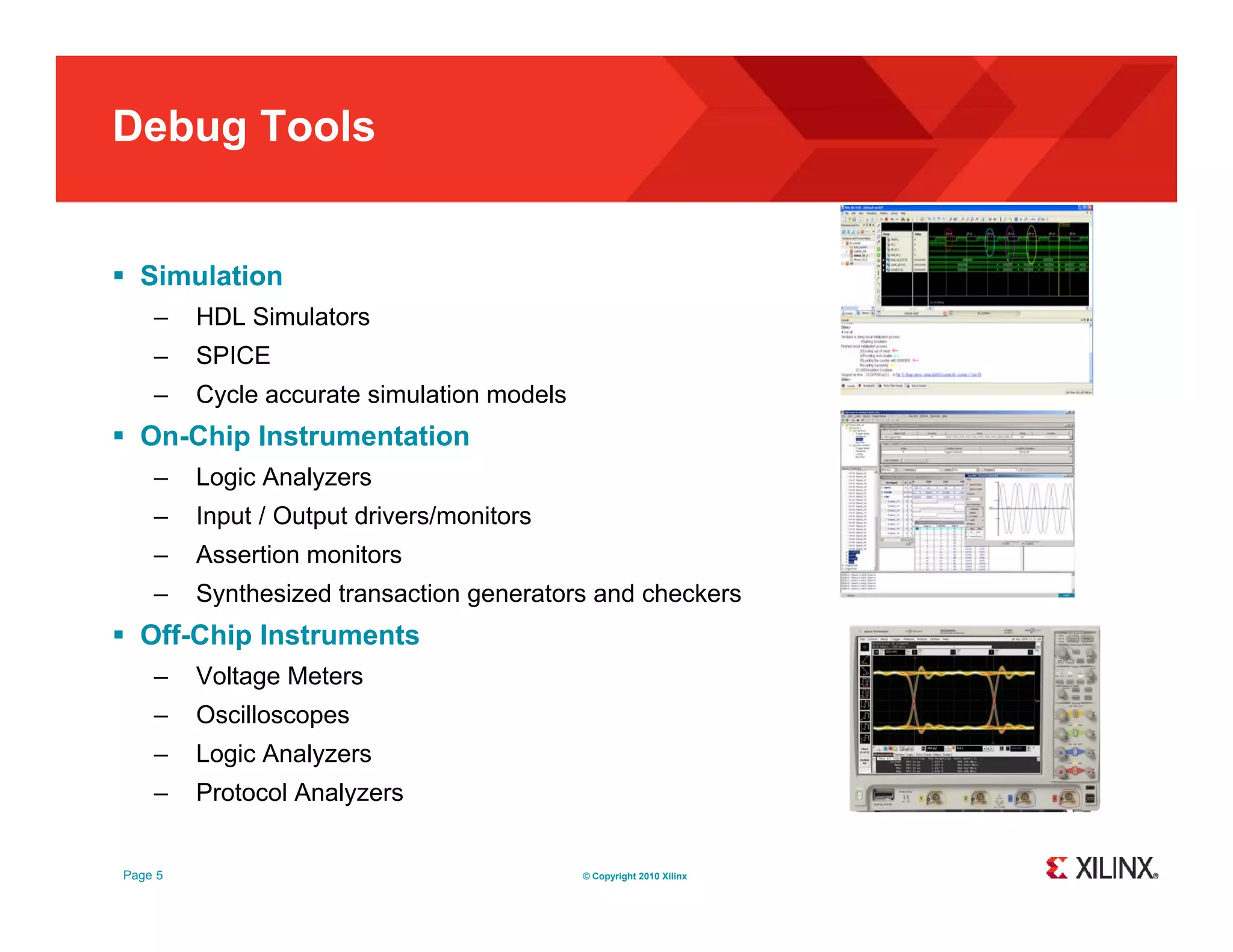
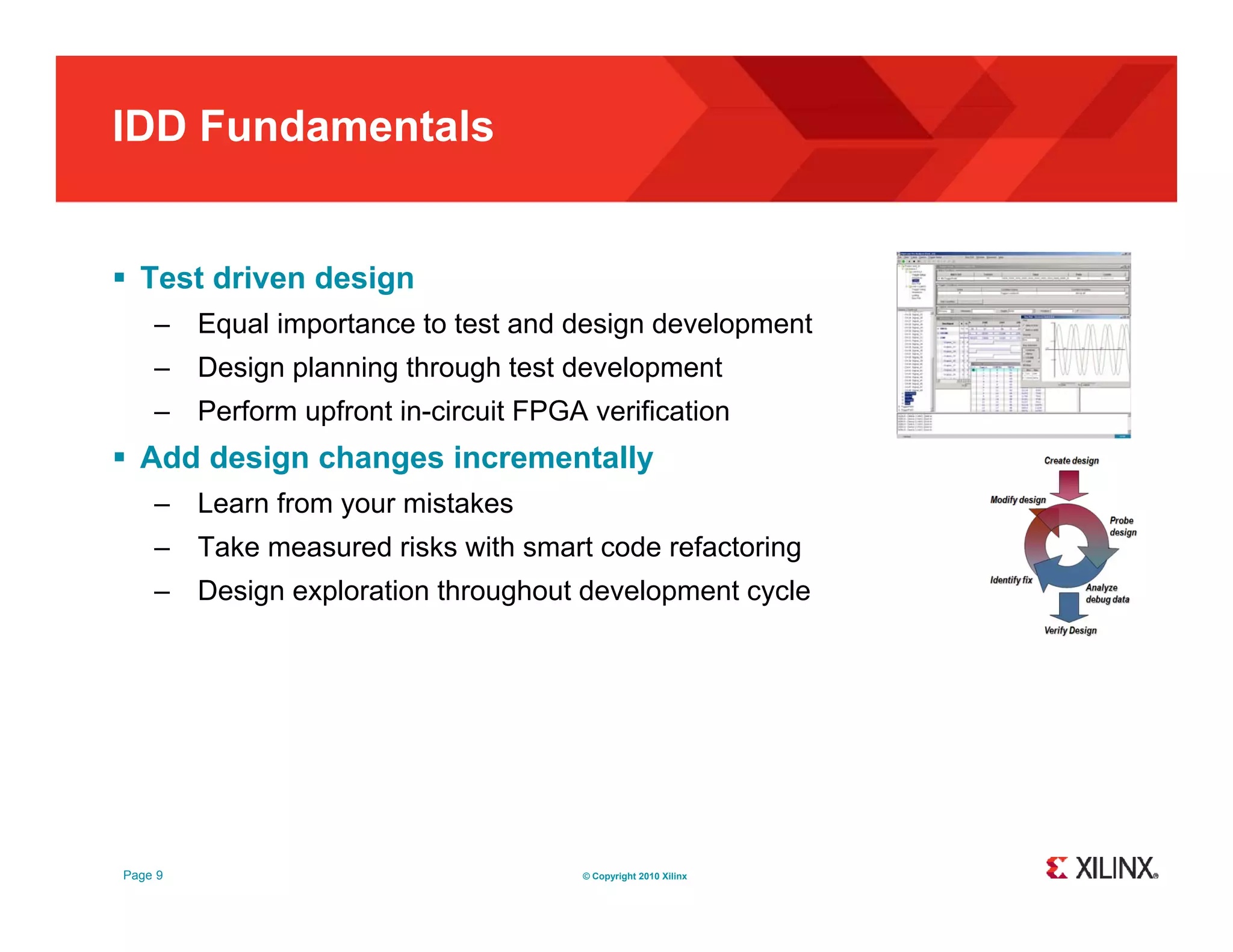
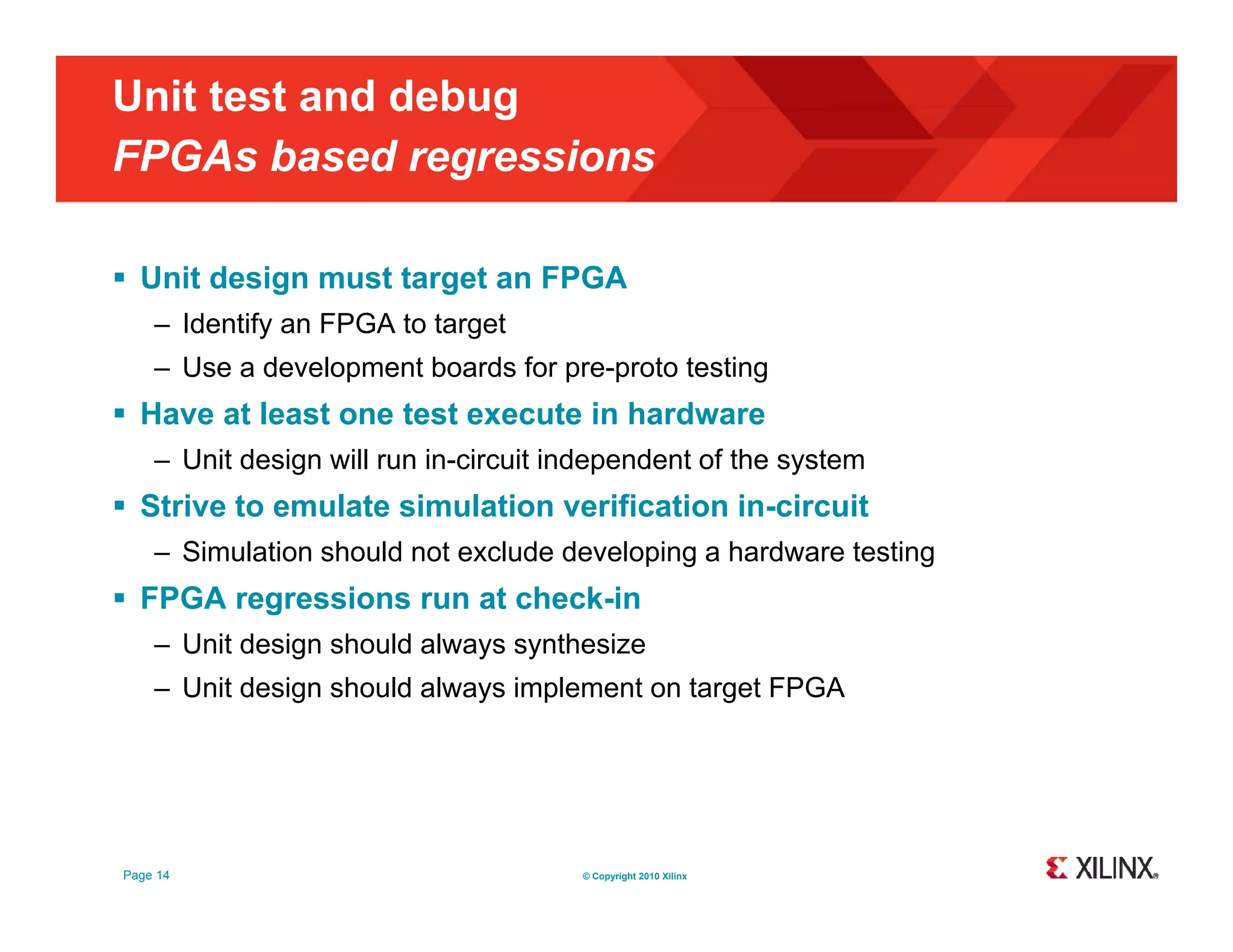
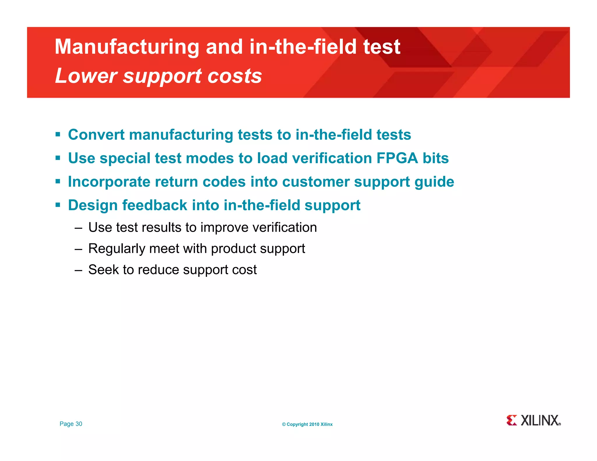
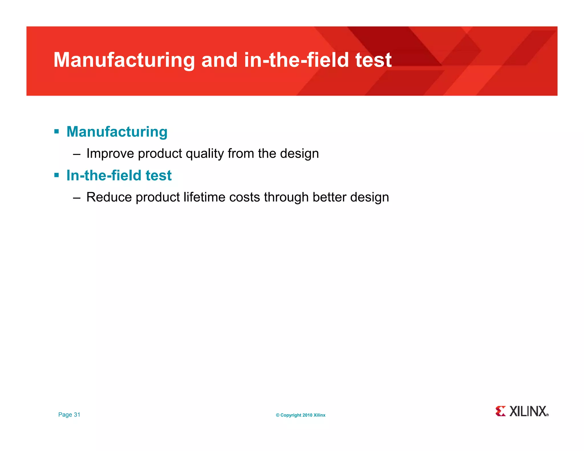
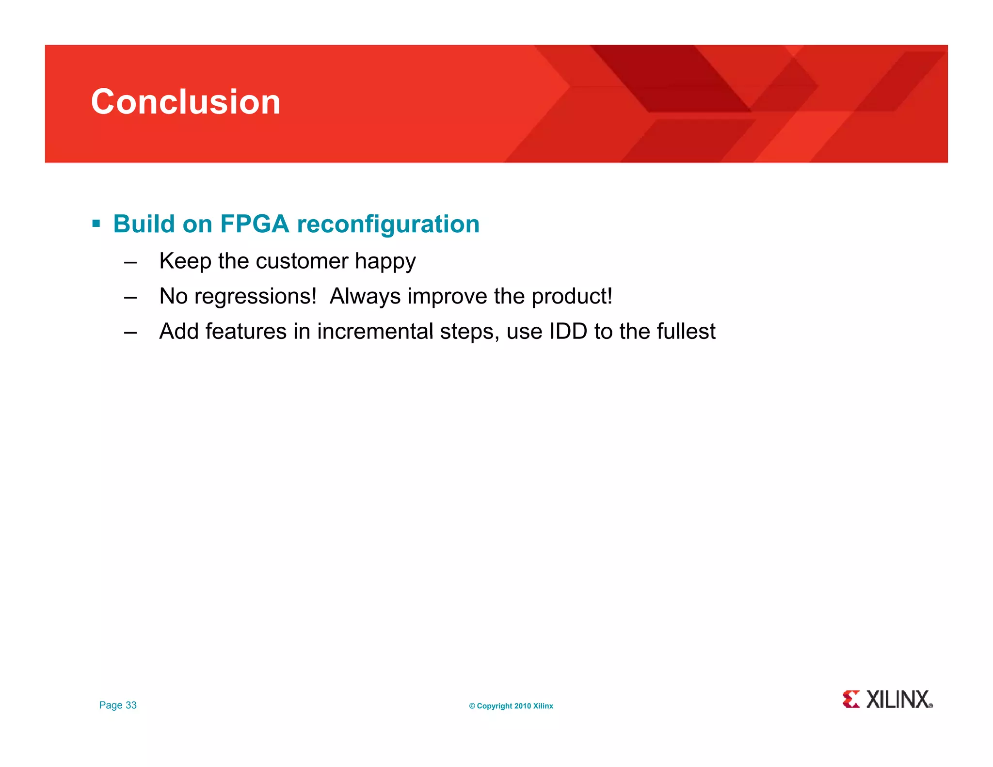

The document discusses mastering FPGA design through effective debugging techniques. It emphasizes incremental design and debug using test-driven development. Debug tools include simulation, on-chip instrumentation, and off-chip instruments. The root of bugs is in the design, so debugging should be done concurrently with designing. System integration focuses on verifying IP interfaces using unit test harnesses. Manufacturing testing validates high-speed links and system connectivity, while in-field tests lower support costs. Overall, the key is building on FPGA reconfiguration, taking advantage of in-circuit testing, seeking design perfection through simplicity, and sharing knowledge.