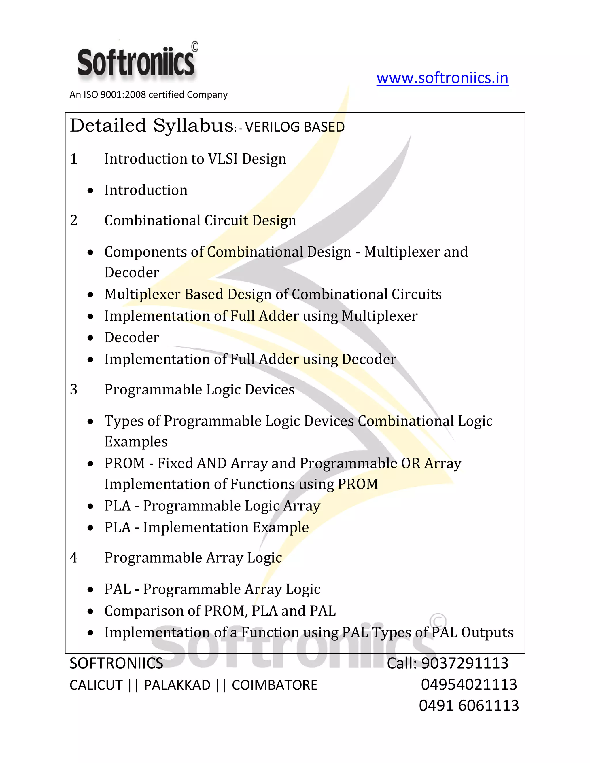
www.softroniics.in An ISO 9001:2008 certified Company SOFTRONIICS Call: 9037291113 CALICUT || PALAKKAD || COIMBATORE 04954021113 0491 6061113 Detailed Syllabus: - VERILOG BASED 1 Introduction to VLSI Design Introduction 2 Combinational Circuit Design Components of Combinational Design - Multiplexer and Decoder Multiplexer Based Design of Combinational Circuits Implementation of Full Adder using Multiplexer Decoder Implementation of Full Adder using Decoder 3 Programmable Logic Devices Types of Programmable Logic Devices Combinational Logic Examples PROM - Fixed AND Array and Programmable OR Array Implementation of Functions using PROM PLA - Programmable Logic Array PLA - Implementation Example 4 Programmable Array Logic PAL - Programmable Array Logic Comparison of PROM, PLA and PAL Implementation of a Function using PAL Types of PAL Outputs
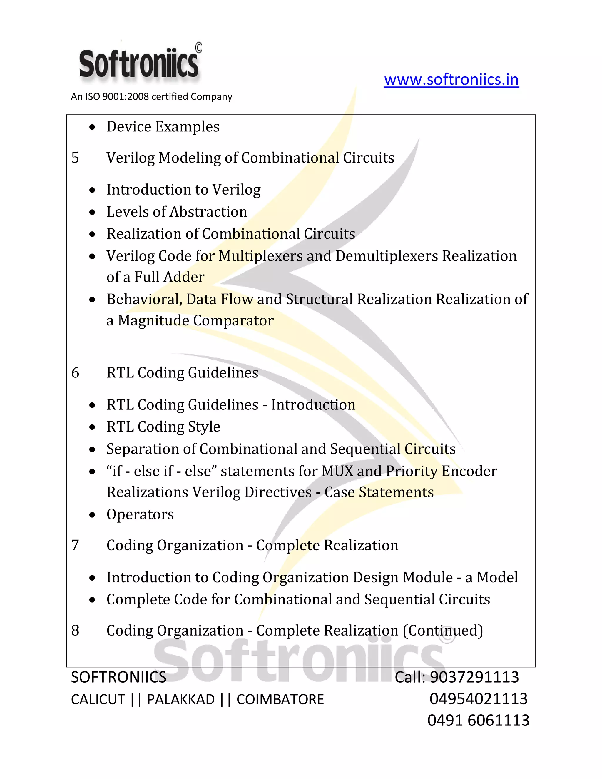
www.softroniics.in An ISO 9001:2008 certified Company SOFTRONIICS Call: 9037291113 CALICUT || PALAKKAD || COIMBATORE 04954021113 0491 6061113 Device Examples 5 Verilog Modeling of Combinational Circuits Introduction to Verilog Levels of Abstraction Realization of Combinational Circuits Verilog Code for Multiplexers and Demultiplexers Realization of a Full Adder Behavioral, Data Flow and Structural Realization Realization of a Magnitude Comparator 6 RTL Coding Guidelines RTL Coding Guidelines - Introduction RTL Coding Style Separation of Combinational and Sequential Circuits “if - else if - else” statements for MUX and Priority Encoder Realizations Verilog Directives - Case Statements Operators 7 Coding Organization - Complete Realization Introduction to Coding Organization Design Module - a Model Complete Code for Combinational and Sequential Circuits 8 Coding Organization - Complete Realization (Continued)
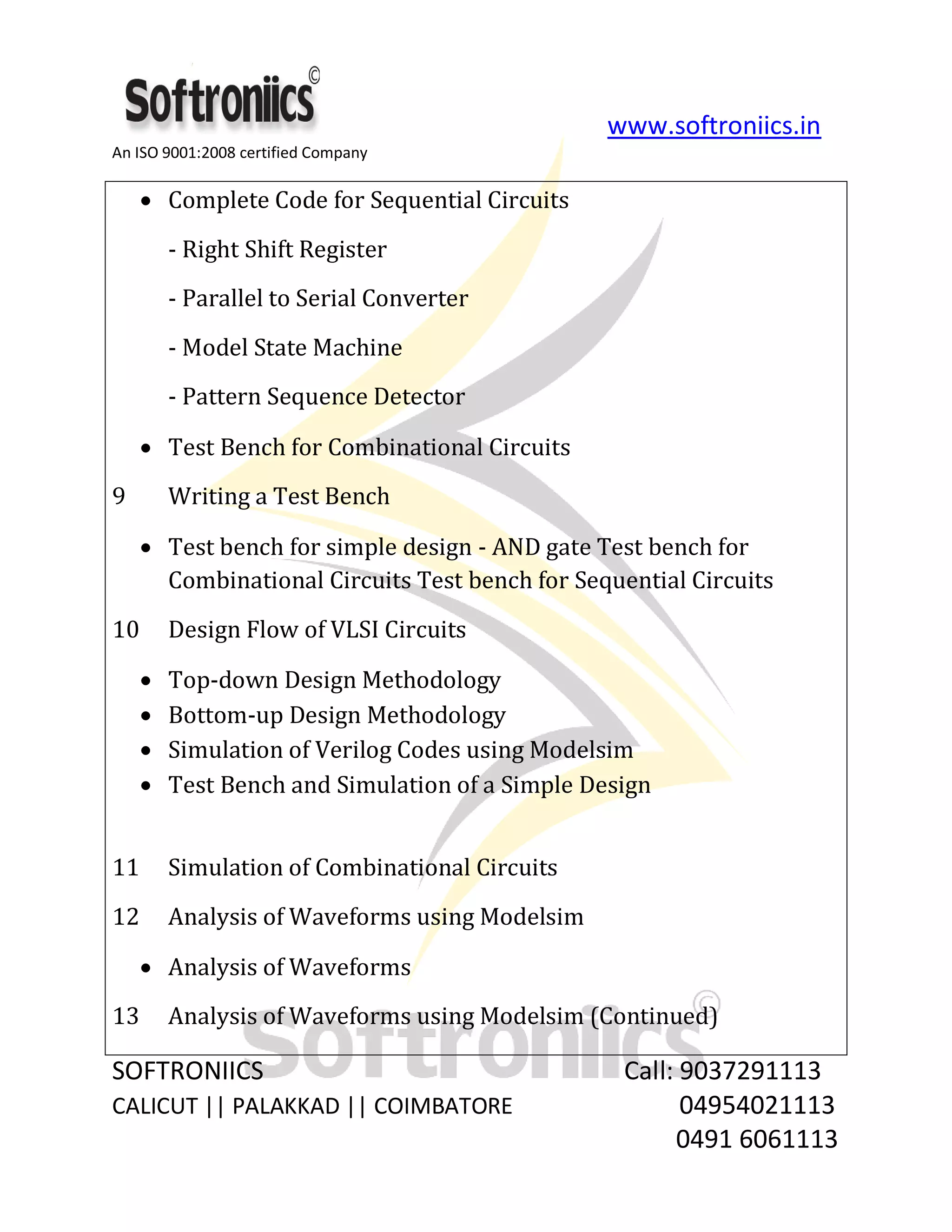
www.softroniics.in An ISO 9001:2008 certified Company SOFTRONIICS Call: 9037291113 CALICUT || PALAKKAD || COIMBATORE 04954021113 0491 6061113 Complete Code for Sequential Circuits - Right Shift Register - Parallel to Serial Converter - Model State Machine - Pattern Sequence Detector Test Bench for Combinational Circuits 9 Writing a Test Bench Test bench for simple design - AND gate Test bench for Combinational Circuits Test bench for Sequential Circuits 10 Design Flow of VLSI Circuits Top-down Design Methodology Bottom-up Design Methodology Simulation of Verilog Codes using Modelsim Test Bench and Simulation of a Simple Design 11 Simulation of Combinational Circuits 12 Analysis of Waveforms using Modelsim Analysis of Waveforms 13 Analysis of Waveforms using Modelsim (Continued)
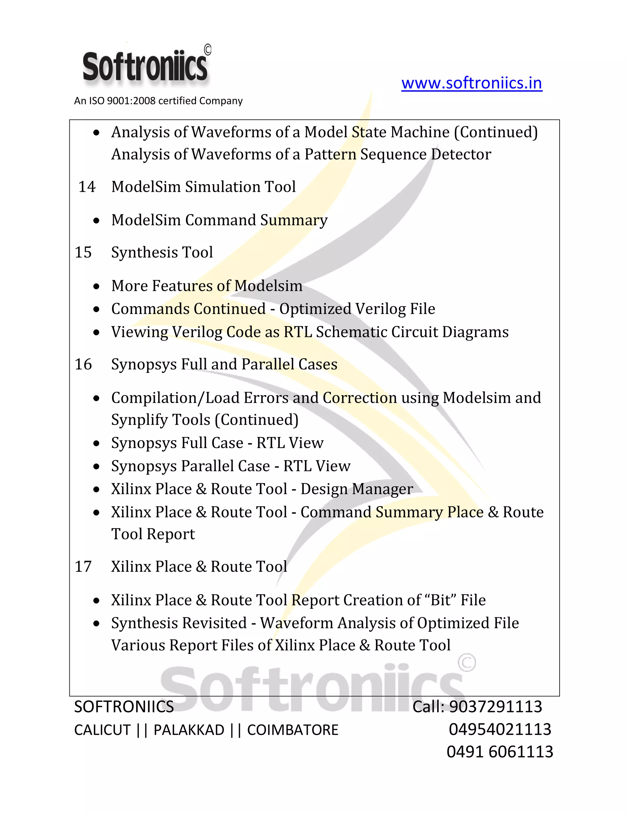
www.softroniics.in An ISO 9001:2008 certified Company SOFTRONIICS Call: 9037291113 CALICUT || PALAKKAD || COIMBATORE 04954021113 0491 6061113 Analysis of Waveforms of a Model State Machine (Continued) Analysis of Waveforms of a Pattern Sequence Detector 14 ModelSim Simulation Tool ModelSim Command Summary 15 Synthesis Tool More Features of Modelsim Commands Continued - Optimized Verilog File Viewing Verilog Code as RTL Schematic Circuit Diagrams 16 Synopsys Full and Parallel Cases Compilation/Load Errors and Correction using Modelsim and Synplify Tools (Continued) Synopsys Full Case - RTL View Synopsys Parallel Case - RTL View Xilinx Place & Route Tool - Design Manager Xilinx Place & Route Tool - Command Summary Place & Route Tool Report 17 Xilinx Place & Route Tool Xilinx Place & Route Tool Report Creation of “Bit” File Synthesis Revisited - Waveform Analysis of Optimized File Various Report Files of Xilinx Place & Route Tool
www.softroniics.in An ISO 9001:2008 certified Company SOFTRONIICS Call: 9037291113 CALICUT || PALAKKAD || COIMBATORE 04954021113 0491 6061113 18 Advanced Features of Xilinx Project Navigator Place and Route and Back Annotation Using Xilinx Project Navigator - Command Summary of Navigator 19. Introduction to FPGA Kit 20. Familiarizing with FPGA Kit

Vlsi course syllabus verilog language

  • 1.
    www.softroniics.in An ISO 9001:2008certified Company SOFTRONIICS Call: 9037291113 CALICUT || PALAKKAD || COIMBATORE 04954021113 0491 6061113 Detailed Syllabus: - VERILOG BASED 1 Introduction to VLSI Design Introduction 2 Combinational Circuit Design Components of Combinational Design - Multiplexer and Decoder Multiplexer Based Design of Combinational Circuits Implementation of Full Adder using Multiplexer Decoder Implementation of Full Adder using Decoder 3 Programmable Logic Devices Types of Programmable Logic Devices Combinational Logic Examples PROM - Fixed AND Array and Programmable OR Array Implementation of Functions using PROM PLA - Programmable Logic Array PLA - Implementation Example 4 Programmable Array Logic PAL - Programmable Array Logic Comparison of PROM, PLA and PAL Implementation of a Function using PAL Types of PAL Outputs
  • 2.
    www.softroniics.in An ISO 9001:2008certified Company SOFTRONIICS Call: 9037291113 CALICUT || PALAKKAD || COIMBATORE 04954021113 0491 6061113 Device Examples 5 Verilog Modeling of Combinational Circuits Introduction to Verilog Levels of Abstraction Realization of Combinational Circuits Verilog Code for Multiplexers and Demultiplexers Realization of a Full Adder Behavioral, Data Flow and Structural Realization Realization of a Magnitude Comparator 6 RTL Coding Guidelines RTL Coding Guidelines - Introduction RTL Coding Style Separation of Combinational and Sequential Circuits “if - else if - else” statements for MUX and Priority Encoder Realizations Verilog Directives - Case Statements Operators 7 Coding Organization - Complete Realization Introduction to Coding Organization Design Module - a Model Complete Code for Combinational and Sequential Circuits 8 Coding Organization - Complete Realization (Continued)
  • 3.
    www.softroniics.in An ISO 9001:2008certified Company SOFTRONIICS Call: 9037291113 CALICUT || PALAKKAD || COIMBATORE 04954021113 0491 6061113 Complete Code for Sequential Circuits - Right Shift Register - Parallel to Serial Converter - Model State Machine - Pattern Sequence Detector Test Bench for Combinational Circuits 9 Writing a Test Bench Test bench for simple design - AND gate Test bench for Combinational Circuits Test bench for Sequential Circuits 10 Design Flow of VLSI Circuits Top-down Design Methodology Bottom-up Design Methodology Simulation of Verilog Codes using Modelsim Test Bench and Simulation of a Simple Design 11 Simulation of Combinational Circuits 12 Analysis of Waveforms using Modelsim Analysis of Waveforms 13 Analysis of Waveforms using Modelsim (Continued)
  • 4.
    www.softroniics.in An ISO 9001:2008certified Company SOFTRONIICS Call: 9037291113 CALICUT || PALAKKAD || COIMBATORE 04954021113 0491 6061113 Analysis of Waveforms of a Model State Machine (Continued) Analysis of Waveforms of a Pattern Sequence Detector 14 ModelSim Simulation Tool ModelSim Command Summary 15 Synthesis Tool More Features of Modelsim Commands Continued - Optimized Verilog File Viewing Verilog Code as RTL Schematic Circuit Diagrams 16 Synopsys Full and Parallel Cases Compilation/Load Errors and Correction using Modelsim and Synplify Tools (Continued) Synopsys Full Case - RTL View Synopsys Parallel Case - RTL View Xilinx Place & Route Tool - Design Manager Xilinx Place & Route Tool - Command Summary Place & Route Tool Report 17 Xilinx Place & Route Tool Xilinx Place & Route Tool Report Creation of “Bit” File Synthesis Revisited - Waveform Analysis of Optimized File Various Report Files of Xilinx Place & Route Tool
  • 5.
    www.softroniics.in An ISO 9001:2008certified Company SOFTRONIICS Call: 9037291113 CALICUT || PALAKKAD || COIMBATORE 04954021113 0491 6061113 18 Advanced Features of Xilinx Project Navigator Place and Route and Back Annotation Using Xilinx Project Navigator - Command Summary of Navigator 19. Introduction to FPGA Kit 20. Familiarizing with FPGA Kit