Download to read offline
![International Research Journal of Engineering and Technology (IRJET) e-ISSN: 2395-0056 Volume: 06 Issue: 06 | June 2019 www.irjet.net p-ISSN: 2395-0072 © 2019, IRJET | Impact Factor value: 7.211 | ISO 9001:2008 Certified Journal | Page 652 Design and Verification of APB Protocol by using System Verilog and Universal Verification Methodology Vaishnavi R.K1, Bindu.S2, Sheik Chandbasha3 1M.Tech, Dept of ECE, B.N.M Institute of Technology, Bangalore, India 2Professor, Dept of ECE, B.N.M Institute of Technology, Bangalore, India 3D &V Engineer, SION Semiconductors, Bangalore, India ---------------------------------------------------------------------***---------------------------------------------------------------------- Abstract - The huge progress of VLSI technology enables the integration of millions of transistor on a single chip called System on chip (SOC).The SOC (system on chip) uses AMBA (Advanced Microcontroller Bus Architecture) as on chip bus protocol. APB (Advanced Peripheral Bus) is one of components of AMBA bus Architecture. In this paper we present the total Design and Verification of AMBA-APB Protocol for SOC Applications. AMBA Bus basically has many components like AHB, ASB, AXI etc which are high performance bus used to interface with low performance bus like APB. APB uses low peripheral bandwidth and is used to connect with slaves like UART, TIMER, Keypad and INTERRUPT CONTROLLER etc. The traditional way of verification is simulation based. As the technology improved complexity of IC’s has been increased. Hence time spent in verification also been increased. This paper mainly focuses on design of APB protocol in Verilog and Verifying in two languages such as System Verilog and Universal Verification Methodology (UVM). Key Words: SOC, AMBA, APB, AXI, ASB 1. INTRODUCTION In the Earlier stages of microcontroller devices AMBA bus was used, but now it is extensively used in many parts of ASIC and FPGA devices, together with in the applications processors which are used in modern mobile devices. APB (Advanced peripheral bus) is basically used to connect with low peripheral devices such as UART, TIMER, KEYPAD and INTERRUPT CONTROLLER etc. which requires low bandwidth.APB has unpiplined also it is used to interface to low bandwidth peripherals which don’t require for high performance. Every transitions are associated with the rising edge of clock therefore it is simple to integrate APB with any other peripherals. AMBA is an open standard, on-chip interconnect specification for the purpose of connecting and managing functional blocks in a System-on-Chip (SOC). It helps in right first time development of the multiprocessor designs with large number of controllers and peripherals[1]. Figure 1 shows the AMBA bus Architecture. Basically it consist of two components namely Advanced high performance bus (AHB), or Advanced System bus (ASB) and Advanced peripheral bus (APB). So the components requiring higher bandwidth like High Bandwidth on chip RAM, High performance ARM processor, High Bandwidth Memory Interface and DMA bus master are connected to the AHB or ASB. AMBA APB is low bandwidth and low performance bus. So, the components requiring lower bandwidth like the peripheral devices such as UART, Keypad, Timer and PIO (Peripheral Input Output) devices are connected to the APB[2]. The bridge connects the high performance AHB or ASB bus to the APB bus. So, for APB the bridge acts as the master and all the devices connected on the APB bus acts as the slave. The component on the high performance bus initiates the transactions and transfer them to the peripherals connected on the APB. So, at a time the bridge is used for communication between the high performance bus and the peripheral devices. Figure 1: AMBA bus Architecture I. APB block diagram 1.1.1 APB Bridge/Master Figure 2: APB Master/Bridge APB is a component of AMBA Hierarchy Bus and it is used to connect with the low peripheral devices. AMBA-APB usually consists of APB Bridge/master and APB slave .and it can be used to interface with many number of slaves[3]. Figure 2 shows the Block diagram of APB bridge/Master](https://image.slidesharecdn.com/irjet-v6i6200-191116041450/75/IRJET-Design-and-Verification-of-APB-Protocol-by-using-System-Verilog-and-Universal-Verification-Methodology-1-2048.jpg)
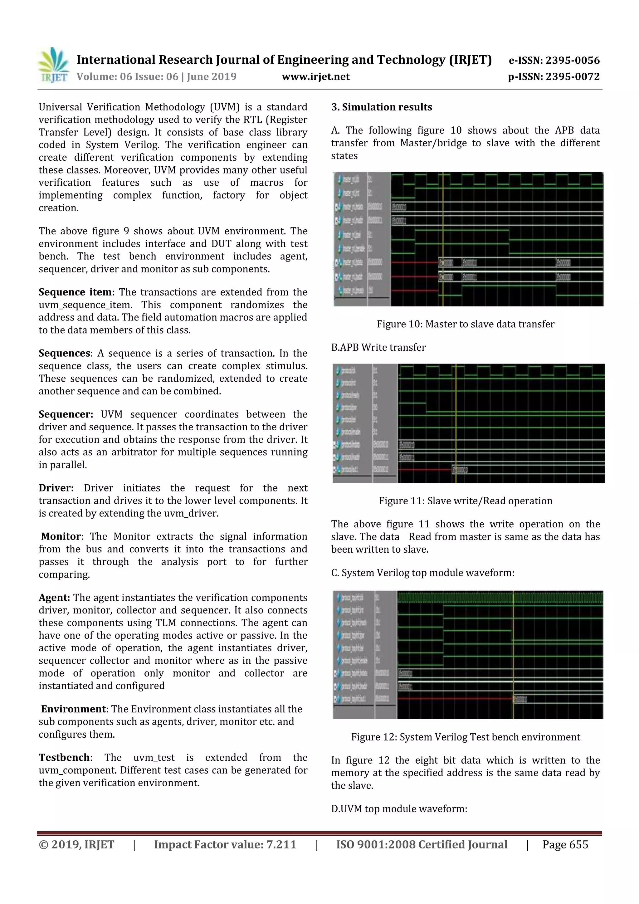
![International Research Journal of Engineering and Technology (IRJET) e-ISSN: 2395-0056 Volume: 06 Issue: 06 | June 2019 www.irjet.net p-ISSN: 2395-0072 © 2019, IRJET | Impact Factor value: 7.211 | ISO 9001:2008 Certified Journal | Page 653 and APB slave. APB bridge is just bus master on AMBA APB. In addition, the APB bridge is also a slave on the high- level system bus. APB Master description: APB Bridge converts the data and address from System bus transfer to APB and performance the following functions. latch the address and holds it valid throughout the transfer. Decodes the address and generates a peripheral select, PSELx. just one select signal can be active during a transfer. Drives the data onto the APB for a write transfer. Drives the APB data onto the system bus for a read transfer[3]. 1.1.2 APB Slave APB Slave have a simple, yet flexible interface and it can be used to interface many slaves. And it performance the subsequent functions. Figure 3:APB Slave Diagram APB Slave description: on either rising edge of PCLK, when PSEL is HIGH on the rising edge of PENABLE, when PSEL is HIGH. The select signal PSELx, the address PADDR and the write signal PWRITE can be combined to determine which register should be updated by the write operation For read transfers the data can be driven on to the data bus when PWRITE is LOW and both PSELx and PENABLE are HIGH. While PADDR is used to determine which register should be read[4]. 1.2 OPERATING STATUS OF AN APB The figure 4 shows the operating status of an APB which represent the activity of peripheral. Figure 4: Operating status of APB Operating status of an APB can be described in three states. IDLE: This will be the default state where there is no transfer of data. SETUP: within this state appropriate PSLELx signal is asserted, bus only remains in the SETUP state for one clock cycle and will always move to the ENABLE state on the next rising edge of the clock. ENABLE/ACCESS: In the ENABLE state PENABLE signal is asserted. The address, write and select signals all remain stable during the transition from the SETUP to ENABLE state. The ENABLE state also only lasts for a single clock cycle and after this state the bus will depart to the IDLE state if no further transfers are required. Alternatively, if another transfer be to follow then the bus will move directly to the SETUP state. It is acceptable for the address, write and select signals to glitch during a transition from the ENABLE to SETUP states[5]. Write cycle: During the write transfer operation, the PSEL, PWRITE, PADDR and PWDATA signals are asserted at the T1 clock edge which is called the SETUP cycle. At the next rising edge of the clock T2, the PENABLE signal and PREADY signal are asserted. This is called the ACCESS cycle. At the clock edge T3, PENABLE signal is disabled and if further data transfer is required, a high to low transition occurs on the PREADY signal.](https://image.slidesharecdn.com/irjet-v6i6200-191116041450/75/IRJET-Design-and-Verification-of-APB-Protocol-by-using-System-Verilog-and-Universal-Verification-Methodology-2-2048.jpg)
![International Research Journal of Engineering and Technology (IRJET) e-ISSN: 2395-0056 Volume: 06 Issue: 06 | June 2019 www.irjet.net p-ISSN: 2395-0072 © 2019, IRJET | Impact Factor value: 7.211 | ISO 9001:2008 Certified Journal | Page 654 Figure 5: APB write Cycle Read Cycle: During the read operation, the PSEL, PENABLE, PWRITE, PADDR signals are asserted at the clock edge T1 (SETUP cycle). At the clock edge T2, (ACCESS cycle), the PENABLE, PREADY are asserted and PRDATA is also read during this phase. Figure 6: APB Read cycle 2. Verification Verification is the important part in the VLSI technology. Because it is used to find out the bugs in the RTL design at the earliest stage so the overall design should not prove destructive. So here we are creating an environment in System Verilog and UVM methodology for the APB design. The main purpose of creating verification environment is to generate the stimulus to DUT (design under test), and check the results to verify that the function is correct. So that test cases can be modified or added by referring the coverage report. Figure 7: position of RTL verification in VLSI design flow 2.1. System Verilog Environment: Figure 8: System Verilog Environment System Verilog is a special hardware verification language to be used in function verification. It provides the high- level data structures available in object-oriented languages, such as C++. These data structures enable a higher level of abstraction and modeling of complex data types. The System Verilog also provides constructs necessary for modeling hardware concepts such as cycles, tri-state values, wires, just like Verilog hardware languages. So System Verilog can be used to simulate the HDL design and verify them by high level test cas[6]. The above figure 8 shows System Verilog environment. The environment includes DUT written in Verilog and System Verilog test bench which include System Verilog interface, simulation module and test program. In system Verilog test bench, the generator is used to create constrained random test vectors. These vectors are sent to the driver, and then can simulate the DUT. The monitor generates verification reports on states, transactions and model messages. Scoreboard checks the results and with this any changes in the modification required that can be made. The advantage of System Verilog is object oriented programming with that it can greatly enhance the reusability of test bench components. The interface is used to join the DUT and the System Verilog test bench which includes the test program. B.UVM Environment Figure 9: UVM Environment](https://image.slidesharecdn.com/irjet-v6i6200-191116041450/75/IRJET-Design-and-Verification-of-APB-Protocol-by-using-System-Verilog-and-Universal-Verification-Methodology-3-2048.jpg)
![International Research Journal of Engineering and Technology (IRJET) e-ISSN: 2395-0056 Volume: 06 Issue: 06 | June 2019 www.irjet.net p-ISSN: 2395-0072 © 2019, IRJET | Impact Factor value: 7.211 | ISO 9001:2008 Certified Journal | Page 656 Figure 13: UVM Test bench environment The above figure 13 shows the UVM test bench waveform where the data written by the master is same as the data read by the slave UVM report summary: Figure 14: UVM report summary UVM report provides the results obtained after simulation of UVM test bench. Figure 14 shows the report generated after running all the UVM phases. UVM_INFO in the report says that there are fifty six information messages. The total summary explains the design is error free and will not produce fatal error since UVM_ERROR, UVM_WARNING and UVM_FATAL is equal to zero. 4. CONCLUSION This paper gives an overview of the AMBA bus architecture and discusses the APB bus in detail. The APB bus is designed using the Verilog HDL according to the specification and is verified using in System Verilog and Universal Verification Methodology. The simulation results show that the data read from a particular memory location is same as the data written to the given memory location. Hence, the design is functionally correct. The UVM report summary also ensures the functional correctness of the design. REFERENCES [1] Heli Shah, Chinmay Modi “Design & Implementation of Advance Peripheral Bus Protocol” IJSEAS - Volume-1, Issue-3, June 201 [2] Shankar, Dipti Girdhar “Design and Verification of AMBA APB Protocol” International Journal of Computer Applications (0975 – 8887) Volume 95– No.21, June 2014. [3] Chenghai Ma, Zhijun Liu, Xiaoyue Ma, “Design and Implementation of APB Bridge based AMBA 4.0,IEEE 2013. [4] ARM “An AMBA Specification Overview V1.0”. [5] Guoliang Ma and RuRe, “Design and Implementation of an Advanced DMA Controller an AMBA based SOC, IEEE 201. [6] Han Ke, Deng Zhongliang,Shu Qiong “Verification of AMBA bus Model using System Verilog” The Eighth International Conference on Electronic Measurement and Instruments IEEE 2011](https://image.slidesharecdn.com/irjet-v6i6200-191116041450/75/IRJET-Design-and-Verification-of-APB-Protocol-by-using-System-Verilog-and-Universal-Verification-Methodology-5-2048.jpg)

This document describes the design and verification of an AMBA APB protocol using System Verilog and Universal Verification Methodology (UVM). It begins with an introduction to AMBA and the APB bus protocol. The APB design is created in Verilog and consists of an APB bridge/master and APB slaves. The design is then verified using System Verilog and UVM testbenches. Simulation waveforms and UVM reports show the data written by the master is correctly read by the slave, indicating the APB protocol is functioning as intended.
Introduction to APB within AMBA, its design for SOCs, and its usage with peripheral devices.
Description of APB master and slave functionalities, data/address conversion and transfer processes.
Details on write and read cycles in the APB, including signal assertions and operational flow.
Introduction to System Verilog and UVM methodologies for verifying the design under test.
Simulation results showing data transfer correctness in UVM and System Verilog environments.