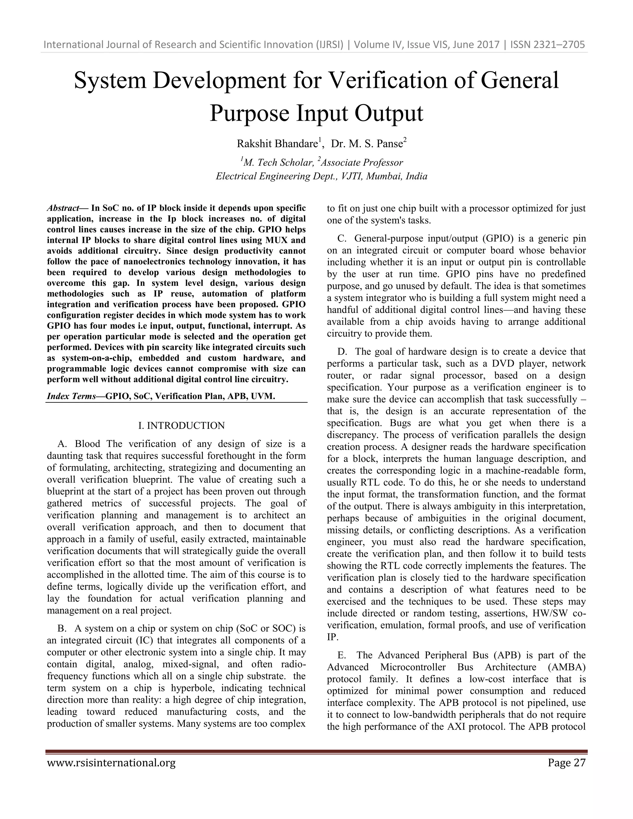
The document discusses the design and verification of general-purpose input/output (GPIO) systems within system-on-chip (SoC) environments, emphasizing the importance of GPIO pins for facilitating digital control lines and reducing circuitry complexity. It outlines the verification methodologies needed to ensure the accuracy of SoC designs, highlighting the use of scripting languages and verification frameworks like SystemVerilog and UVM. Additionally, it addresses the evolution in SoC technology driven by market demands and technological advancements, illustrating the roles GPIOs play in modern integrated circuits.
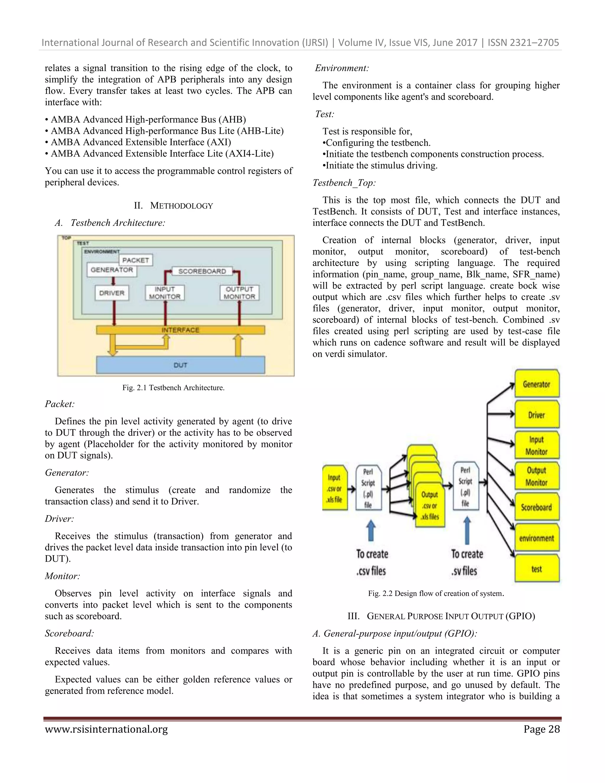
![International Journal of Research and Scientific Innovation (IJRSI) | Volume IV, Issue VIS, June 2017 | ISSN 2321–2705 www.rsisinternational.org Page 30 Fig. 4.3 Input Datasheet. V. TOOLS Verification environment is needed for a new design, or for a design revision with significant changes, it is important to objectively look at the shortcomings of the existing verification environment and expected productivity gain with the new methodology and determine the best solution. In our case we need to find an optimum balance between re-usability of our legacy Verilog environment and the resource utilization along with limited timelines in adopting the new methodology. This can be accomplished by reusing the knowledge /legacy code from an earlier project along with an upgrade to a new methodology provided with the verification language, that is A. SystemVerilog. The feature-set of SystemVerilog can be divided into two distinct roles: 1.SystemVerilog for RTL design is an extension of Verilog-2005; all features of that language are available in SystemVerilog. 2.SystemVerilog for verification uses extensive object- oriented programming techniques and is more closely related to Java than Verilog. B. Universal Verification Methodology (UVM) It is a standardized methodology for verifying integrated circuit designs. UVM is derived mainly from the OVM (Open Verification Methodology) which was, to a large part, based on the eRM (e Reuse Methodology) for the e Verification Language developed by Verisity Design in 2001. The UVM class library brings much automation to the SystemVerilog language such as sequences and data automation features (packing, copy, compare) etc., and unlike the previous methodologies developed independently by the simulator vendors, is an Accellera standard with support from multiple vendors: Aldec, Cadence, Mentor, and Synopsys. C. scripting script language is a programming language that supports scripts, programs written for a special run-time environment that automate the execution of tasks that could alternatively be executed one-by-one by a human operator.[1] Scripting languages are often interpreted (rather than compiled). Primitives are usually the elementary tasks or API calls, and the language allows them to be combined into more complex programs. Environments that can be automated through scripting include software applications, web pages within a web browser, the shells of operating systems (OS), embedded systems, as well as numerous games. A scripting language can be viewed as a domain-specific language for a particular environment; in the case of scripting an application, this is also known as an extension language. Scripting languages are also sometimes referred to as very high-level programming languages, as they operate at a high level of abstraction, or as control languages, particularly for job control languages on mainframes. The term "scripting language" is also used loosely to refer to dynamic high-level general-purpose languages, such as Perl, Tcl, and Python, with the term "script" often used for small programs (up to a few thousand lines of code) in such languages, or in domain-specific languages such as the text- processing languages sed and AWK. Some of these languages were originally developed for use within a particular environment, and later developed into portable domain- specific or general-purpose languages. Conversely, many general-purpose languages have dialects that are used as scripting languages. This article discusses scripting languages in the narrow sense of languages for a specific environment. Embedded software plays a critical role in driving today’s SoC verification at various stages. With growing SoC complexity and evolving processor architecture, it has become increasingly difficult to perform SoC debug activities. What is needed is a simultaneous view of both hardware and software to help designers efficiently and effectively advance their debug productivity. A sophisticated waveform viewer that can display and analyze activities in time series Fast Signal Database (FSDB) A high-performance waveform comparison engine that identifies discrepancies between files Source code / browser that facilitates coordination between source code and hierarchical browser Flexible circuit diagram and block diagram that can display logic and connection relationship using familiar symbols Intuitive state transition diagram that can grasp the operation of the state machine VI. RESULTS Fig. 6.1 Implementation of scripting.](https://image.slidesharecdn.com/27-32-170709024257/75/System-Development-for-Verification-of-General-Purpose-Input-Output-4-2048.jpg)
![International Journal of Research and Scientific Innovation (IJRSI) | Volume IV, Issue VIS, June 2017 | ISSN 2321–2705 www.rsisinternational.org Page 31 Mapping of required source and destination from the respective functional mode from the input Datasheet is done using Scripting Language i.e. PERL. The script extracts required source and destination for respective peripherals which automates the result. Input to the script can be .csv file or .xls file and generates the results also in .csv or xls format. Fig. 6.2 Result of Input Mode. Fig. 6.3 Result of Output Mode. Fig. 6.4 Result of Functional Mode. Fig. 6.5 Result of Functional Mode. VII. CONCLUSION The System-on-Chip (SoC) industry has developed rapidly over the last fifteen years from producing VLSI devices that integrated a processor and a few memory and peripheral components onto a single chip to today’s high-performance SoCs that incorporate hundreds of IP blocks. This progress is a consequence of Moore’s Law (which enables ever-higher levels of integration) and of market economics (where consumers demand ever-more functionality in smaller, lower- cost products with better battery life). System on a Chip (SoC) integrated circuits make extensive use of general-purpose I/O (GPIO) pins. GPIO controllers provide a variety of functions for peripheral devices, including interrupts, input signaling, and output signaling. A feature of some GPIO controllers is the ability to generate interrupts on both edges of a signal (rising, or Active-High edges, and falling, or Active-Low edges). GPIO helps internal IP blocks to share digital control lines using MUX and avoids additional circuitry. Devices with pin scarcity like integrated circuits such as system-on-a-chip, embedded and custom hardware, and programmable logic devices cannot compromise with size can perform well without additional digital control line circuitry. REFERENCES [1] Chris Spear, Greg Tumbush,”SystemVerilog for Verification: A Guide to Learning the Testbench Language Features”,3rd edition,Springer Science & Business Media, 2012. [2] Sik Kim, Kwang-Hyun Cho, Byeong Min “An efficient GPIO block design methodology using formalized SFR description”, SoC Design Conference (ISOCC), 2011 International. [3] D. Gajski, "Essential Issues for IP Reuse", Proceedings of ASP- DAC, pp. 37-42. [4] C. K. Lennard, "Industrially Proving the SPIRIT Consortium Specifications for Design Chain Integration", Proceedings of DATE 2006, pp. 1-6. [5] K. Cho, "Reusable Platform Design Methodology For SOC Integration And Verification", Proceedings of ISOCC 2008, pp. 1-78. [6] 6W. Kruijtzer, "Industrial IP integration flows based on IP-XACT standards", Proceedings of DATE 2008, pp. 32-37.](https://image.slidesharecdn.com/27-32-170709024257/75/System-Development-for-Verification-of-General-Purpose-Input-Output-5-2048.jpg)
![International Journal of Research and Scientific Innovation (IJRSI) | Volume IV, Issue VIS, June 2017 | ISSN 2321–2705 www.rsisinternational.org Page 32 [7] S. Sarkar, S. Chanclar G, S. Shinde “Effective IP reuse for high quality SOC design”, SOC Conference, 2005. Proceedings. IEEE International. [8] M. Strik, "Subsystem Exchange in a Concurrent Design Process Environment", Proceedings of DATE 2008, pp. 953-958. [9] V. Guide, "SystemVerilog TestBench", Verificationguide.com, 2016. [Online]. Available: http://www.verificationguide.com/p/writing-systemverilog- verification.html. [Accessed: 19- Sep- 2016]. [10] "Typical Verification Flow", Asic-world.com, 2016. [Online]. Available: http://www.asic- world.com/tidbits/typical_verification.html. [Accessed: 19- Sep- 2016]. [11] "Basic UVM | Universal Verification Methodology | Verification Academy", Verificationacademy.com, 2016. [Online]. Available: https://verificationacademy.com/courses/basic-uvm. [Accessed: 19- Sep- 2016]. [12] 12. "UVM (Universal Verification Methodology)", Accellera.org, 2016. [Online]. Available: http://www.accellera.org/activities/vip. [Accessed: 19- Sep- 2016]. [13] "Teach Yourself Perl 5 in 21 days - Table of Contents", Wwwacs.gantep.edu.tr, 2016. [Online]. Available: http://wwwacs.gantep.edu.tr/docs/perl-ebook/. [Accessed: 03- Dec- 2016]. [14] "Perl tutorial", Perl Maven, 2016. [Online]. Available: https://perlmaven.com/perl-tutorial. [Accessed: 03- Dec- 2016]. [15] R. Schwartz, T. Phoenix and B. Foy, “Learning Perl”, 1st ed. Sebastopol, CA: O'Reilly, 2005. [16] "The Perl Programming Language - www.perl.org", Perl.org, 2016. [Online]. Available: https://www.perl.org/. [Accessed: 03- Dec- 2016].](https://image.slidesharecdn.com/27-32-170709024257/75/System-Development-for-Verification-of-General-Purpose-Input-Output-6-2048.jpg)