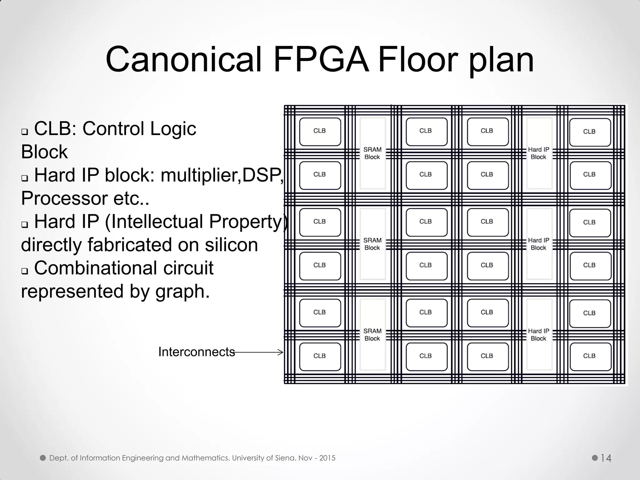
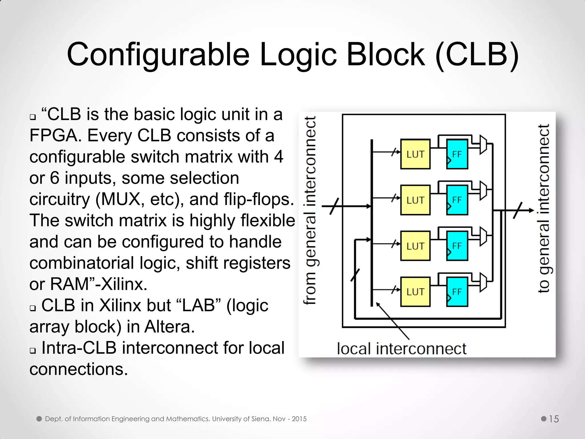
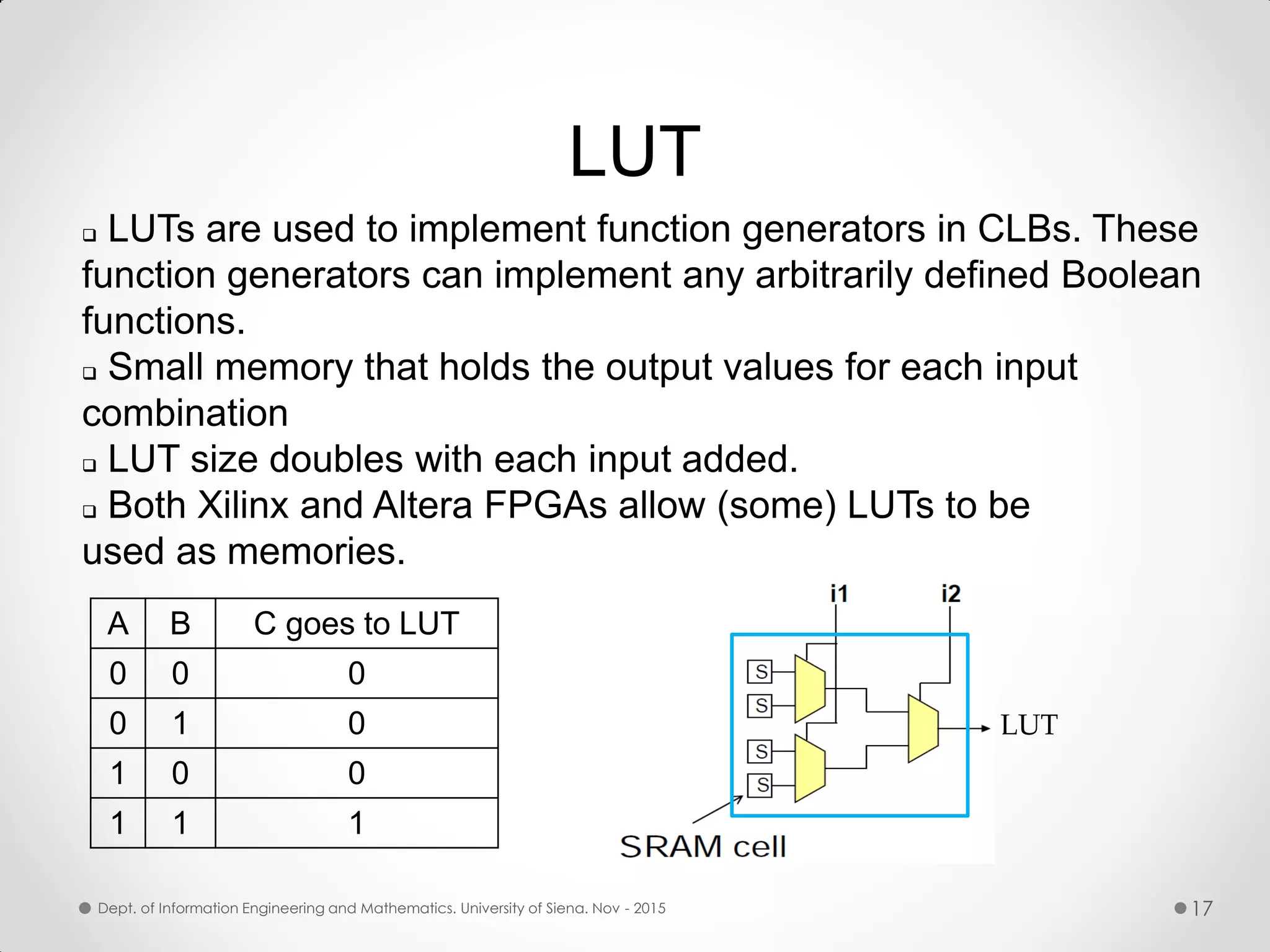
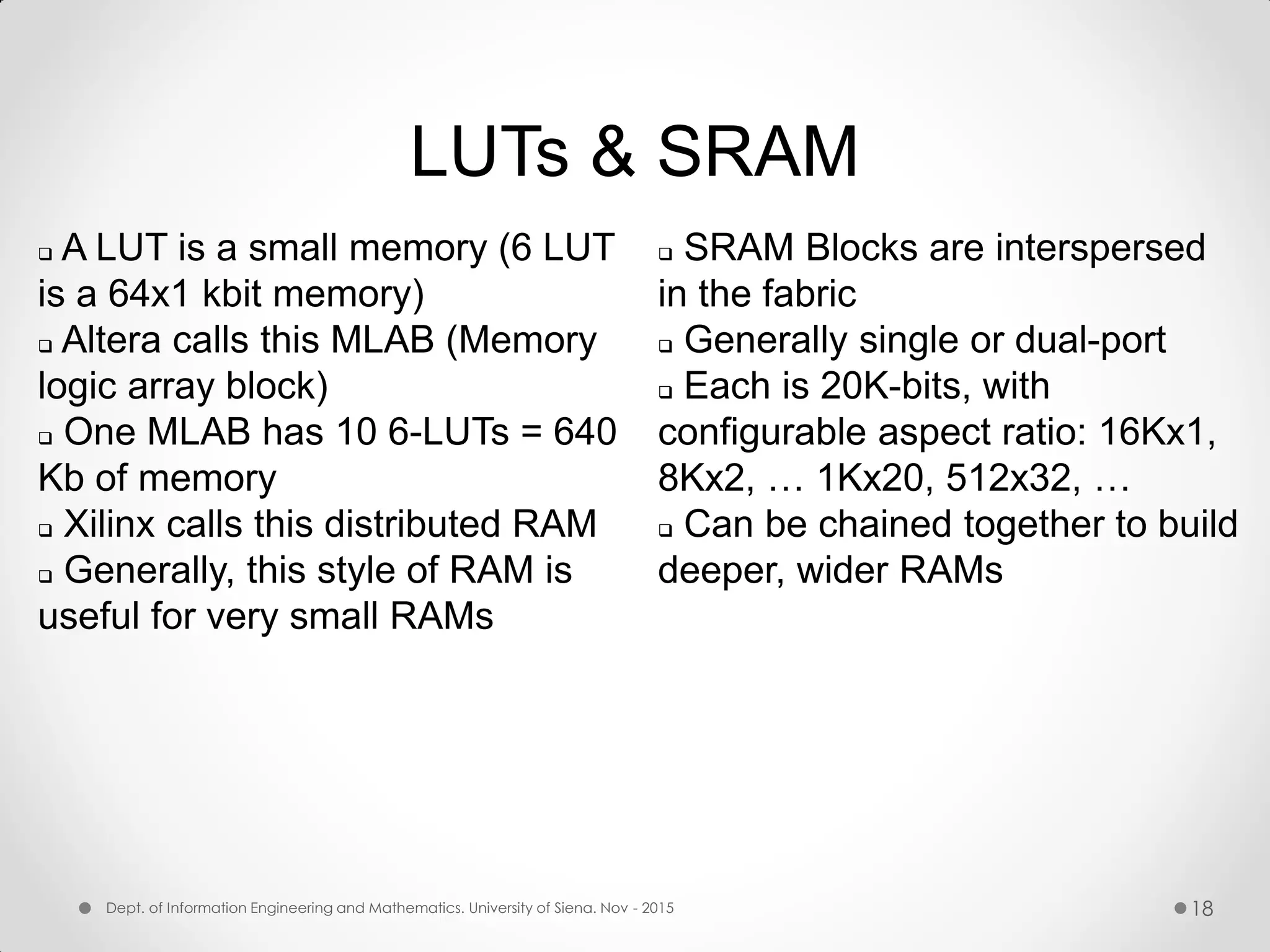
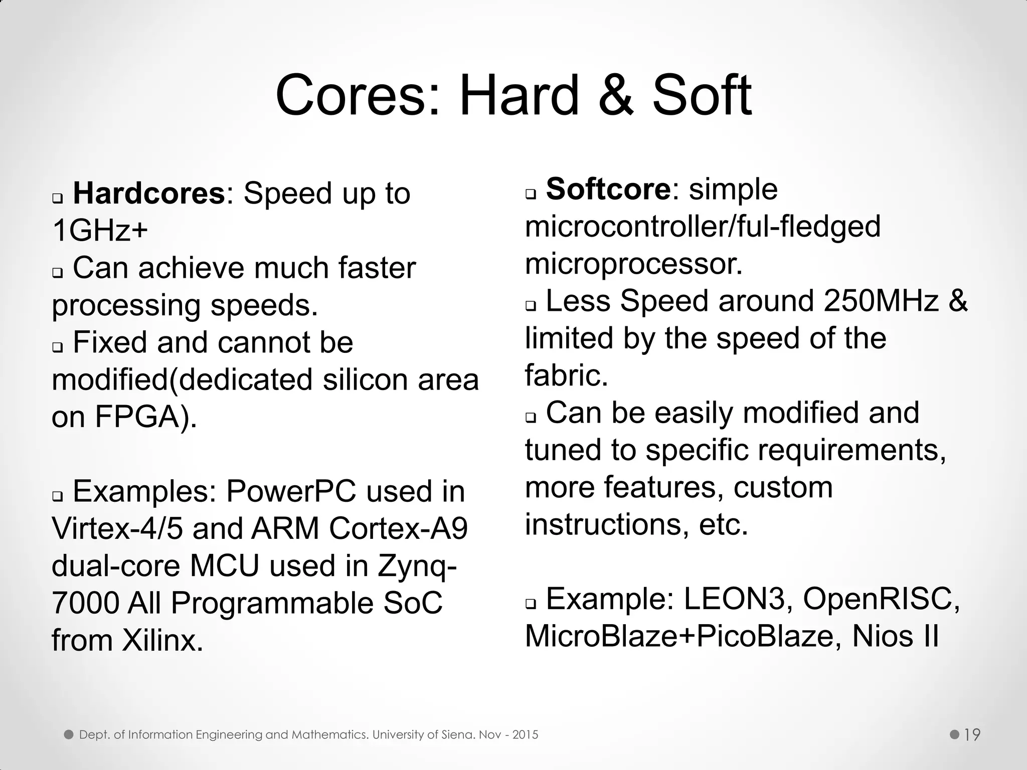
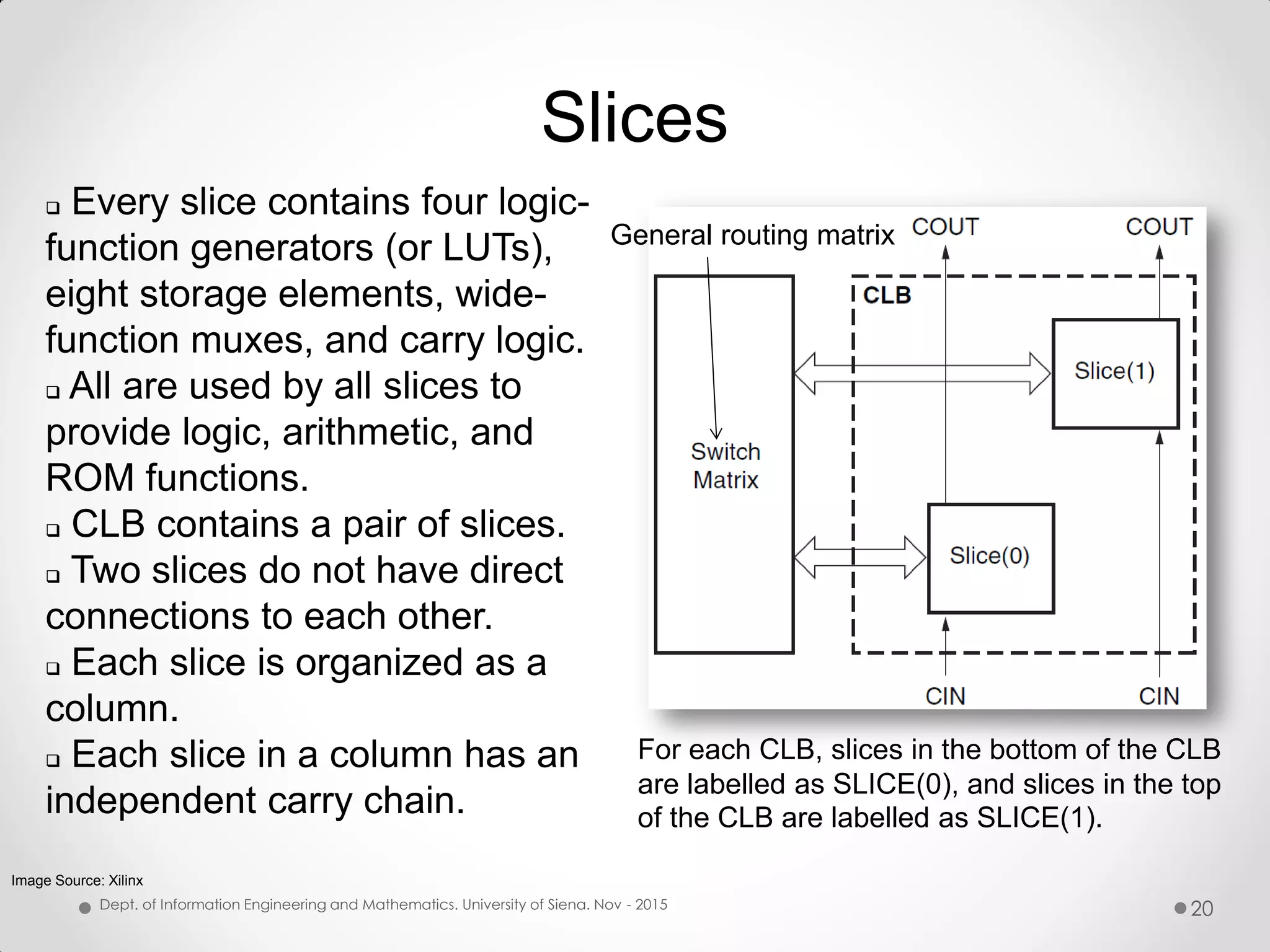
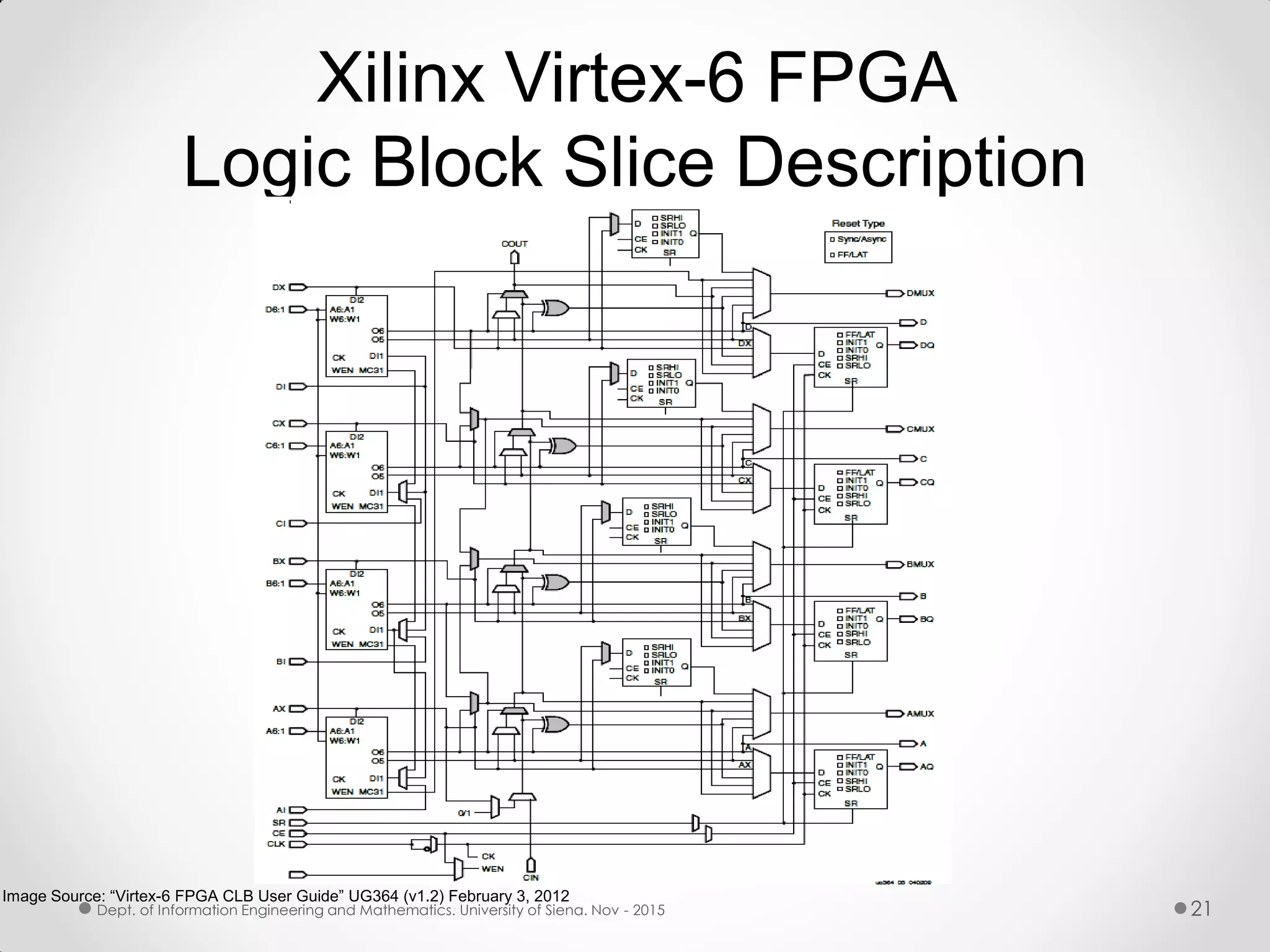
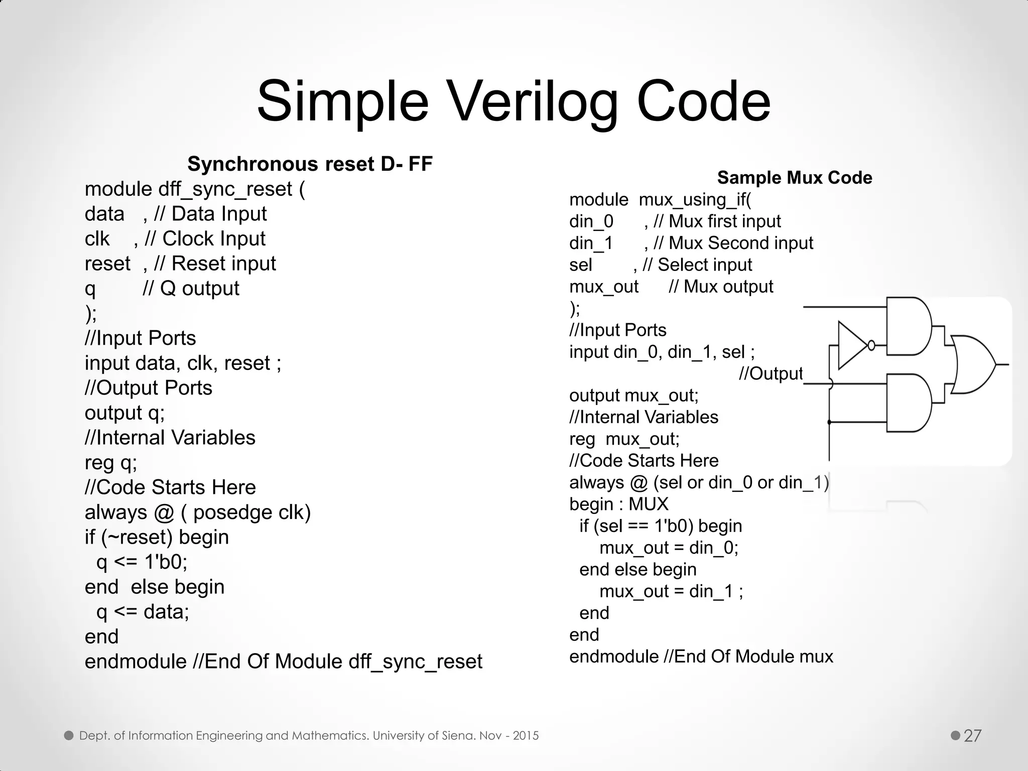
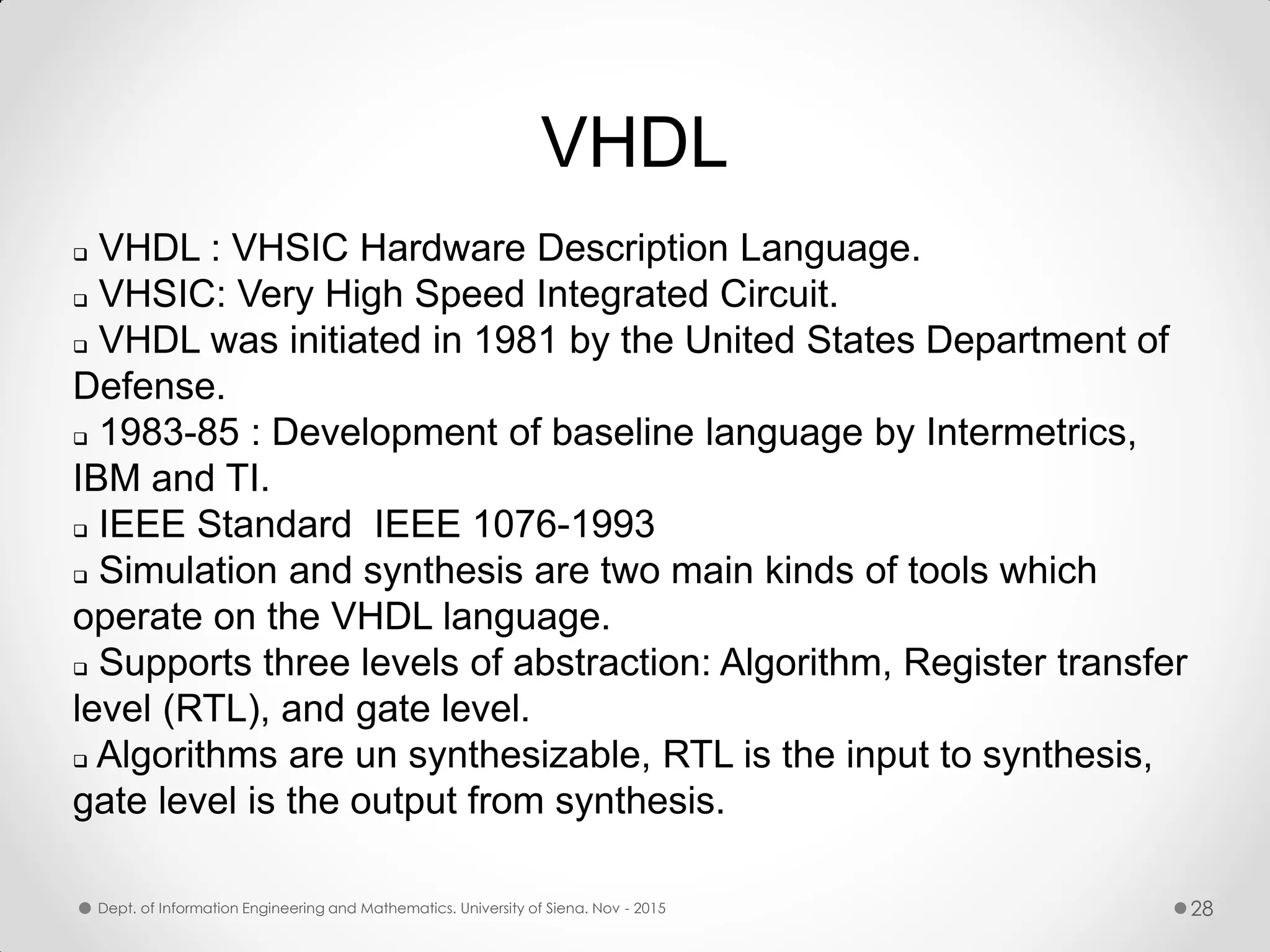
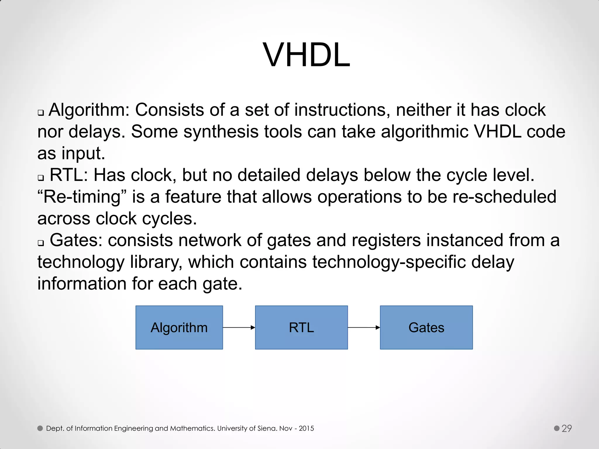
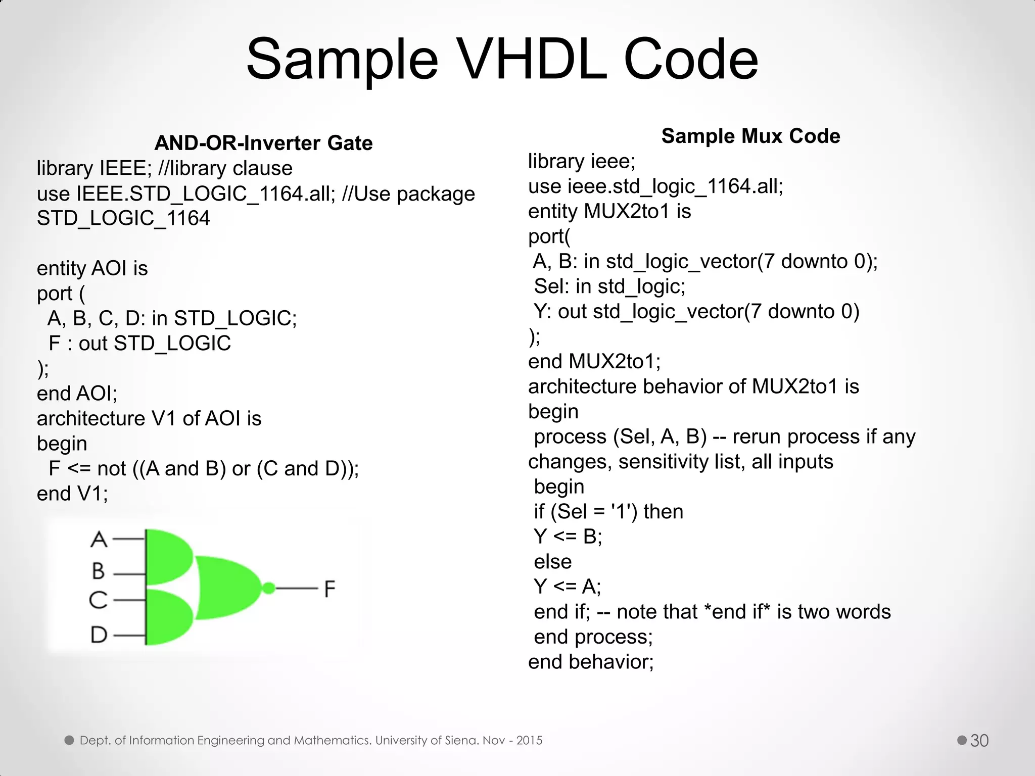
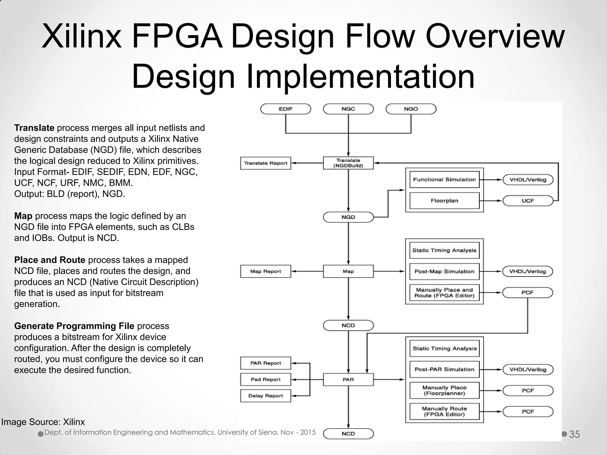
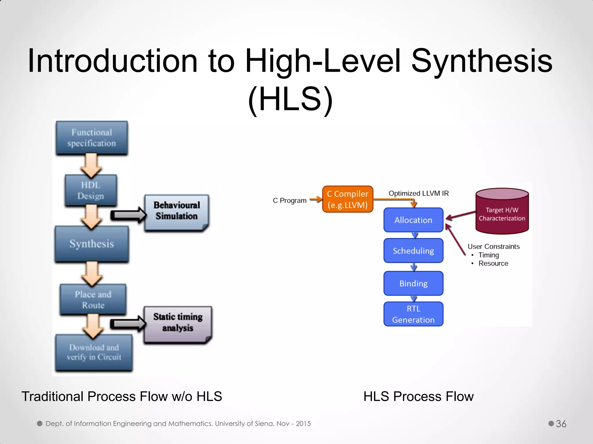
FPGA in a “Nutshell” Presented By: Somnath MAZUMDAR IIIrd Year PhD student University of Siena, Italy
Outline Introduction Architecture Programming Dept. of Information Engineering and Mathematics. University of Siena. Nov - 2015 2
Prerequisites to FPGA Learning • Before to learn: • Basic Boolean operations(AND, OR, NOT, XOR) • Number representations and binary math • Digital Circuits • Programming ability in 'C' or assembler • Bit of microcontroller development experience •To Start with: • Hardware Description Language like VHDL/Verilog • Coding in a programming language like C for rendering ideas into syntax Dept. of Information Engineering and Mathematics. University of Siena. Nov - 2015 3
Birth of FPGA(1975-1985) 1975 : PLA (programmable logic array) made up of programmable AND gate planes and programmable OR gate planes, connected to product a desired output(POS (product of sums), and SOP (sum of products)). 1978 : PAL (programmable array logic) similar to PLA; has one PROM array, a fixed OR plane and a programmable AND plane. 1983 : EEPROM (Electrically EPROM) 1983 : GAL (generic array logic) is completely erasable and re- programmable, but PAL not. 1984 : FLASH (type of EEPROM) non-volatile memory. FLASH memory can be erased in blocks. 6Dept. of Information Engineering and Mathematics. University of Siena. Nov - 2015
Birth of FPGA contd…  1985: First FPGA XC2064 had 64 configurable logic blocks (CLBs), with two three-input lookup tables (LUTs). It offered 800 gates, sold for $55, and was produced on a 2.0µ process. What is a Field Programmable Gate Array (FPGA)? “FPGAs are programmable semiconductor devices that are based around a matrix of Configurable Logic Blocks (CLBs) connected through programmable interconnects. FPGAs can be programmed to the desired application or functionality requirements”-Xilinx. Types of FPGA : 1. One-Time Programmable (OTP) FPGAs 2. SRAM-based (can be reprogrammed as the design evolves).  Company: Altera, Xilinx 7Dept. of Information Engineering and Mathematics. University of Siena. Nov - 2015
Field-Programmable Gate Array  CLB: CLBs contain clusters of LUTs + Registers + arithmetic + other circuitry.  LUTs: LUT (look-up-tables) is a hardware implementation of a truth table.  FPGA is a special kind of chip that is configurable by the end user.  Has programmable logic and can implement any digital circuit.. Dept. of Information Engineering and Mathematics. University of Siena. Nov - 2015 8
But.. why Use FPGA?  Application needs tailored HW  No need to over-provision (Like custom ASIC)  Don’t worry about mistakes it is “Reconfigurable”  Make chip development faster. FPGAs provide significantly more hardware acceleration performance/watt [1] Image Source: Xilinx SDAccel Developer Zone. http://www.xilinx.com/products/design-tools/ software-zone/sdaccel.html. “FPGA-based accelerators can achieve up to 25x better performance per watt and 50-75x latency improvement compared to CPU/GPU implementations while also providing excellent I/O integration (PCI, DDR4 SDRAM interfaces, high-speed Ethernet, etc.)..”[1] Dept. of Information Engineering and Mathematics. University of Siena. Nov - 2015 9
Where are FPGAs Used Today?  Networking, Computer & Storage  Telecom and Wireless  Automotive, Aerospace, Industrial Automation, Military etc… Dept. of Information Engineering and Mathematics. University of Siena. Nov - 2015 10 Do you know?? Microsoft Bing Search built on FPGAs based accelerators
But.. what about Weaknesses  For a specific circuit, relative to a custom ASIC, FPGAs use more area, power and slower  FPGA resources are of a fixed size and have limited flexibility options.  But you may not have the option for “reconfiguration” Metric FPGAvsASIC[1] FPGAvsASIC[2] Area 30-40X 2-20X Delay 3-4X 1.7-3X Dy. Power 12X Static Power 5-90X 2-5X [1] Compares Altera Stratix-II to ST Microelectronics standard cells (90nm technology) [Kuon et. al. (TCAD`07)]. [2] Altera Corp 2006. Dept. of Information Engineering and Mathematics. University of Siena. Nov - 2015 11
 Resource usage of 2-input function vs 3-input function is same 6- input function uses 1 6-LUT; 7 input function uses 2 6-LUTs (double resource usage).  6x6-bit multiply has same DSP usage as 8x8-bit multiply  Similar arguments for memories  The biggest problem with FPGAs used for application acceleration has been programming.  Programming in FPGA is more than programming micro- controller.. Practical Examples Dept. of Information Engineering and Mathematics. University of Siena. Nov - 2015 12
Outline Introduction Architecture Programming Dept. of Information Engineering and Mathematics. University of Siena. Nov - 2015 13
Canonical FPGA Floor plan  CLB: Control Logic Block  Hard IP block: multiplier,DSP, Processor etc..  Hard IP (Intellectual Property) directly fabricated on silicon  Combinational circuit represented by graph. Interconnects Dept. of Information Engineering and Mathematics. University of Siena. Nov - 2015 14
Configurable Logic Block (CLB)  “CLB is the basic logic unit in a FPGA. Every CLB consists of a configurable switch matrix with 4 or 6 inputs, some selection circuitry (MUX, etc), and flip-flops. The switch matrix is highly flexible and can be configured to handle combinatorial logic, shift registers or RAM”-Xilinx.  CLB in Xilinx but “LAB” (logic array block) in Altera.  Intra-CLB interconnect for local connections. Dept. of Information Engineering and Mathematics. University of Siena. Nov - 2015 15
Logic Tile (CLB/LAB) Comparison  Xilinx CLB: 8 6-LUTs, each with 6 inputs  Each LUT can implement any two functions that together use <= 5 inputs  Fast carry circuitry: 1 sum bit / 6-LUT  FFs: 2 FFs / 6-LUT  Altera LAB: 10 6-LUTs, each with 8 inputs  Each LUT can be fractured into two independent 4-LUTs  Fast carry circuitry: 2 sum bits / 6-LUT  FFs: 4 FFs / 6-LUT Dept. of Information Engineering and Mathematics. University of Siena. Nov - 2015 16
LUT  LUTs are used to implement function generators in CLBs. These function generators can implement any arbitrarily defined Boolean functions.  Small memory that holds the output values for each input combination  LUT size doubles with each input added.  Both Xilinx and Altera FPGAs allow (some) LUTs to be used as memories. A B C goes to LUT 0 0 0 0 1 0 1 0 0 1 1 1 LUT Dept. of Information Engineering and Mathematics. University of Siena. Nov - 2015 17
LUTs & SRAM  A LUT is a small memory (6 LUT is a 64x1 kbit memory)  Altera calls this MLAB (Memory logic array block)  One MLAB has 10 6-LUTs = 640 Kb of memory  Xilinx calls this distributed RAM  Generally, this style of RAM is useful for very small RAMs  SRAM Blocks are interspersed in the fabric  Generally single or dual-port  Each is 20K-bits, with configurable aspect ratio: 16Kx1, 8Kx2, … 1Kx20, 512x32, …  Can be chained together to build deeper, wider RAMs Dept. of Information Engineering and Mathematics. University of Siena. Nov - 2015 18
Cores: Hard & Soft  Hardcores: Speed up to 1GHz+  Can achieve much faster processing speeds.  Fixed and cannot be modified(dedicated silicon area on FPGA).  Examples: PowerPC used in Virtex-4/5 and ARM Cortex-A9 dual-core MCU used in Zynq- 7000 All Programmable SoC from Xilinx.  Softcore: simple microcontroller/ful-fledged microprocessor.  Less Speed around 250MHz & limited by the speed of the fabric.  Can be easily modified and tuned to specific requirements, more features, custom instructions, etc.  Example: LEON3, OpenRISC, MicroBlaze+PicoBlaze, Nios II Dept. of Information Engineering and Mathematics. University of Siena. Nov - 2015 19
Slices  Every slice contains four logic- function generators (or LUTs), eight storage elements, wide- function muxes, and carry logic.  All are used by all slices to provide logic, arithmetic, and ROM functions.  CLB contains a pair of slices.  Two slices do not have direct connections to each other.  Each slice is organized as a column.  Each slice in a column has an independent carry chain. Image Source: Xilinx For each CLB, slices in the bottom of the CLB are labelled as SLICE(0), and slices in the top of the CLB are labelled as SLICE(1). Dept. of Information Engineering and Mathematics. University of Siena. Nov - 2015 20 General routing matrix
Xilinx Virtex-6 FPGA Logic Block Slice Description Image Source: “Virtex-6 FPGA CLB User Guide” UG364 (v1.2) February 3, 2012 Dept. of Information Engineering and Mathematics. University of Siena. Nov - 2015 21
I/Os are programmable to operate according to a variety of signaling standards.  All state-of-the-art FPGAs incorporate Multi-gigabit transceivers (MGTs)  High-speed serial I/Os:  Virtex-7 and Stratix V: individual MGTs operable up to 28 Gb/s  Virtex-7 has 2.7 Tb/s peak serial bandwidth FPGA I/O Support Dept. of Information Engineering and Mathematics. University of Siena. Nov - 2015 22
Outline Introduction Architecture Programming Dept. of Information Engineering and Mathematics. University of Siena. Nov - 2015 23
About HDL  HDL : Hardware Description Language  HDL is a collective name for all hardware definition languages (like Verilog, VHDL)  Register-Transfer Level (RTL) is a design abstraction and a way of describing a circuit.  RTL describes flip-flops, latches and how data is transferred in between etc.  You write your RTL level code in an HDL language which then gets translated (by synthesis tools) to gate level description in the same HDL language/target device/process.  A bitstream is a sequence of bits sends to FPGA to perform the needed operations. Dept. of Information Engineering and Mathematics. University of Siena. Nov - 2015
Verilog  Verilog-XL (a logic simulator + hardware description language) is first Verilog HDL developed By Gateway Design Automation in 1980s.  The Verilog HDL is an IEEE standard(IEEE Std. 1364-1995).  SystemVerilog is a huge set of extensions to Verilog.  Verilog and VHDL are two different HDLs.  Why use Verilog? Structural Level(Lower level): gates level Code always synthesizable Functional Level (Higher Level): Gate level, RTL level, high-level behavioural Easier to write, not always synthesizable. Dept. of Information Engineering and Mathematics. University of Siena. Nov - 2015 25
Verilog  Data Types: Basic type: Bit vector Values: 0, 1, X (don't care), Z (high impedance) Example: Binary: 4'b11_10, Hex: 16'h034f, Decimal: 32'd270 Use wire to connect components: Single wire Example: wire my_wire Array of wires : Example: wire[7:0] my_wire) Reg for procedural assignments: Example reg[3:0] accum; // 4 bit “reg”) reg is not necessarily a hardware register Dept. of Information Engineering and Mathematics. University of Siena. Nov - 2015 26
Simple Verilog Code Synchronous reset D- FF module dff_sync_reset ( data , // Data Input clk , // Clock Input reset , // Reset input q // Q output ); //Input Ports input data, clk, reset ; //Output Ports output q; //Internal Variables reg q; //Code Starts Here always @ ( posedge clk) if (~reset) begin q <= 1'b0; end else begin q <= data; end endmodule //End Of Module dff_sync_reset Sample Mux Code module mux_using_if( din_0 , // Mux first input din_1 , // Mux Second input sel , // Select input mux_out // Mux output ); //Input Ports input din_0, din_1, sel ; //Output Ports output mux_out; //Internal Variables reg mux_out; //Code Starts Here always @ (sel or din_0 or din_1) begin : MUX if (sel == 1'b0) begin mux_out = din_0; end else begin mux_out = din_1 ; end end endmodule //End Of Module mux Dept. of Information Engineering and Mathematics. University of Siena. Nov - 2015 27
VHDL  VHDL : VHSIC Hardware Description Language.  VHSIC: Very High Speed Integrated Circuit.  VHDL was initiated in 1981 by the United States Department of Defense.  1983-85 : Development of baseline language by Intermetrics, IBM and TI.  IEEE Standard IEEE 1076-1993  Simulation and synthesis are two main kinds of tools which operate on the VHDL language.  Supports three levels of abstraction: Algorithm, Register transfer level (RTL), and gate level.  Algorithms are un synthesizable, RTL is the input to synthesis, gate level is the output from synthesis. Dept. of Information Engineering and Mathematics. University of Siena. Nov - 2015 28
 Algorithm: Consists of a set of instructions, neither it has clock nor delays. Some synthesis tools can take algorithmic VHDL code as input.  RTL: Has clock, but no detailed delays below the cycle level. “Re-timing” is a feature that allows operations to be re-scheduled across clock cycles.  Gates: consists network of gates and registers instanced from a technology library, which contains technology-specific delay information for each gate. Algorithm RTL Gates VHDL Dept. of Information Engineering and Mathematics. University of Siena. Nov - 2015 29
Sample VHDL Code AND-OR-Inverter Gate library IEEE; //library clause use IEEE.STD_LOGIC_1164.all; //Use package STD_LOGIC_1164 entity AOI is port ( A, B, C, D: in STD_LOGIC; F : out STD_LOGIC ); end AOI; architecture V1 of AOI is begin F <= not ((A and B) or (C and D)); end V1; Sample Mux Code library ieee; use ieee.std_logic_1164.all; entity MUX2to1 is port( A, B: in std_logic_vector(7 downto 0); Sel: in std_logic; Y: out std_logic_vector(7 downto 0) ); end MUX2to1; architecture behavior of MUX2to1 is begin process (Sel, A, B) -- rerun process if any changes, sensitivity list, all inputs begin if (Sel = '1') then Y <= B; else Y <= A; end if; -- note that *end if* is two words end process; end behavior; Dept. of Information Engineering and Mathematics. University of Siena. Nov - 2015 30
Tips on Coding Note: Std_logic_vector used to define a signal of more than 1 bit. In this case A, B and Y are all 8 bits and can be referred to as a vector or as individual components such as A(7), A(6),.. Etc. Process(Sel, A, B) is the sensitivity list. Sel is 1 bit so the syntax is if (Sel = ‘1’) . Rule 1: To synthesize combinational logic using a process, all inputs to the design must appear in the sensitivity list. Rule 2: To synthesize combinational logic using a process, all objects must be assigned under all conditions. Dept. of Information Engineering and Mathematics. University of Siena. Nov - 2015 31
Bits of Advice..  Popular HDL languages are Verilog and VHDL.  There are also vendor-specific ones like AHDL (Altera HDL).  If you're familiar with C/C++ programming, then you should choose Verilog, rather than VHDL. Verilog's syntax is similar to C.  Get a simulator: Open Source: Icarus Verilog (1) is a Verilog simulation and synthesis tool.  Happy Coding!!!  But…as an alternative, you could use high-level synthesis techniques such as: Xilinx's Vivado HLS and Altera's OpenCL solution. 1.http://iverilog.icarus.com/ Dept. of Information Engineering and Mathematics. University of Siena. Nov - 2015 32
Xilinx FPGA Design Flow Overview  Design flow comprises the following steps: Design entry, Design synthesis, Design implementation Xilinx® device program  Design verification: Includes both functional & timing verification, takes places at different points during the design flow. Image Source: Xilinx Dept. of Information Engineering and Mathematics. University of Siena. Nov - 2015 33
Synthesis process checks code syntax and analyze the hierarchy of your design. Resulting netlist is saved to an NGC file (for Xilinx® Synthesis Technology (XST)). Check Syntax process checks the syntax of the selected source file prior to generating a netlist of the design by synthesis or compile. Image Source: Xilinx Xilinx FPGA Design Flow Overview Dept. of Information Engineering and Mathematics. University of Siena. Nov - 2015 34 Core files are EDIF (EDIF (Electronic Design Interchange Format)) NGC files contain both logical design data and constraints.
Xilinx FPGA Design Flow Overview Design Implementation Image Source: Xilinx Dept. of Information Engineering and Mathematics. University of Siena. Nov - 2015 35 Translate process merges all input netlists and design constraints and outputs a Xilinx Native Generic Database (NGD) file, which describes the logical design reduced to Xilinx primitives. Input Format- EDIF, SEDIF, EDN, EDF, NGC, UCF, NCF, URF, NMC, BMM. Output: BLD (report), NGD. Map process maps the logic defined by an NGD file into FPGA elements, such as CLBs and IOBs. Output is NCD. Place and Route process takes a mapped NCD file, places and routes the design, and produces an NCD (Native Circuit Description) file that is used as input for bitstream generation. Generate Programming File process produces a bitstream for Xilinx device configuration. After the design is completely routed, you must configure the device so it can execute the desired function.
Introduction to High-Level Synthesis (HLS) Traditional Process Flow w/o HLS HLS Process Flow Dept. of Information Engineering and Mathematics. University of Siena. Nov - 2015 36
HLS  LLVM: low-level virtual machine  Open-source compiler framework(http://llvm.org)  Used by Apple, NVIDIA, AMD, others  Competitive quality with gcc & performs standard (50+)optimizations  Several HLS tools (LegUp, Altera, Xilinx) are built as “back-ends” of LLVM  LLVM will compile C code into a control flow graph (CFG) Dept. of Information Engineering and Mathematics. University of Siena. Nov - 2015 37
HLS  Control Flow Graph:  Composed of basic blocks  Basic block: is a sequence of instructions (shift, add, divide, xor, and,branch, call, etc.) terminated with exactly one branch  Can be represented by an acyclic data flow graph  HLS tools (Both built within LLVM compiler framework)  Xilinx Vivado HLS (Language support: C, C++, SystemC)  Altera OpenCL SDK Open Computing Language (OpenCL) is the first open, royalty-free standard for cross-platform, parallel programming. https://www.khronos.org/opencl/ Dept. of Information Engineering and Mathematics. University of Siena. Nov - 2015 38
HLS: Key Aspect  Scheduling: Defines the HW’s finite state machine How to assign the computations of a program into the hardware time steps? Or Which operations can be scheduled in the same time step? Or Which operations are dependent on others?  SDC[1]: System of Difference Constraints : formulate scheduling as a mathematical optimization problem (linear program (LP)).  Variables: For each operation(op) to schedule, create a variable(var). var will hold the cycle # in which each op is scheduled. 1. Cong, Zhang, “An efficient and versatile scheduling algorithm based on SDC formulation”. DAC 2006: 433-438. Dept. of Information Engineering and Mathematics. University of Siena. Nov - 2015 39
 Constraints:  Dependency Constraints : The subtract can only happen after the add and shift,  Clock Period Constraints : For each chain of dependant operations in DFG, find the path delayD.  Resource Constraints: Allow up to 2 load/store operations in a cycle  Binding: e.g. Bind the following scheduled operations.  Loop Pipelining : Overlap execution of adjacent loop iterations. Can be combined with loop unrolling for (int i = 0; i < N; i++) { a[i] = b[i] + c[i] } Each iteration requires: • 2 loads from memory • 1 store • No dependencies between iterations HLS: Key Aspect Dept. of Information Engineering and Mathematics. University of Siena. Nov - 2015 40
HLS Pragma Examples PIPELINE: pipeline a loop UNROLL: unroll a loop ARRAY_PARTITION: partition an array into multiple arrays for parallel access ARRAY_MAP: map multiple arrays into a single array INLINE: inline a function LATENCY: set the scheduling latency ALLOCATION: set the # of HW instances of something Dept. of Information Engineering and Mathematics. University of Siena. Nov - 2015 41
Recommended Readings Book: Advanced FPGA Design: Architecture, Implementation, and Optimization 1st Edition. Circuit Design with VHDL by Volnei A. Pedroni Embedded Systems Design with Platform FPGAs: Principles and Practices 1st Edition by Ronald Sass (Author), Andrew G. Schmidt (Author). Verilog HDL : A Guide to Digital Design and Synthesis by Samir Palnitkar Advanced Chip Design, Practical Examples in Verilog by Mr Kishore K Mishra The Verilog Hardware Description Language by Philip R. Moorby, Donald E. Thomas Lists of Books: http://www.verilog.com/v-books.html Tutorials: http://www.fpga4fun.com/HDL%20tutorials.html. Dept. of Information Engineering and Mathematics. University of Siena. Nov - 2015 42
Notice Slides has been made from the slides of Prof. Jason Anderson (University of Toronto, Canada) and also with the help of Xilinx manuals. 43
Dept. of Information Engineering and Mathematics. University of Siena. Nov - 2015 44

FPGA In a Nutshell

  • 1.
    FPGA in a“Nutshell” Presented By: Somnath MAZUMDAR IIIrd Year PhD student University of Siena, Italy
  • 2.
    Outline Introduction Architecture Programming Dept. of InformationEngineering and Mathematics. University of Siena. Nov - 2015 2
  • 3.
    Prerequisites to FPGALearning • Before to learn: • Basic Boolean operations(AND, OR, NOT, XOR) • Number representations and binary math • Digital Circuits • Programming ability in 'C' or assembler • Bit of microcontroller development experience •To Start with: • Hardware Description Language like VHDL/Verilog • Coding in a programming language like C for rendering ideas into syntax Dept. of Information Engineering and Mathematics. University of Siena. Nov - 2015 3
  • 4.
    Birth of FPGA(1975-1985) 1975: PLA (programmable logic array) made up of programmable AND gate planes and programmable OR gate planes, connected to product a desired output(POS (product of sums), and SOP (sum of products)). 1978 : PAL (programmable array logic) similar to PLA; has one PROM array, a fixed OR plane and a programmable AND plane. 1983 : EEPROM (Electrically EPROM) 1983 : GAL (generic array logic) is completely erasable and re- programmable, but PAL not. 1984 : FLASH (type of EEPROM) non-volatile memory. FLASH memory can be erased in blocks. 6Dept. of Information Engineering and Mathematics. University of Siena. Nov - 2015
  • 5.
    Birth of FPGAcontd…  1985: First FPGA XC2064 had 64 configurable logic blocks (CLBs), with two three-input lookup tables (LUTs). It offered 800 gates, sold for $55, and was produced on a 2.0µ process. What is a Field Programmable Gate Array (FPGA)? “FPGAs are programmable semiconductor devices that are based around a matrix of Configurable Logic Blocks (CLBs) connected through programmable interconnects. FPGAs can be programmed to the desired application or functionality requirements”-Xilinx. Types of FPGA : 1. One-Time Programmable (OTP) FPGAs 2. SRAM-based (can be reprogrammed as the design evolves).  Company: Altera, Xilinx 7Dept. of Information Engineering and Mathematics. University of Siena. Nov - 2015
  • 6.
    Field-Programmable Gate Array CLB: CLBs contain clusters of LUTs + Registers + arithmetic + other circuitry.  LUTs: LUT (look-up-tables) is a hardware implementation of a truth table.  FPGA is a special kind of chip that is configurable by the end user.  Has programmable logic and can implement any digital circuit.. Dept. of Information Engineering and Mathematics. University of Siena. Nov - 2015 8
  • 7.
    But.. why UseFPGA?  Application needs tailored HW  No need to over-provision (Like custom ASIC)  Don’t worry about mistakes it is “Reconfigurable”  Make chip development faster. FPGAs provide significantly more hardware acceleration performance/watt [1] Image Source: Xilinx SDAccel Developer Zone. http://www.xilinx.com/products/design-tools/ software-zone/sdaccel.html. “FPGA-based accelerators can achieve up to 25x better performance per watt and 50-75x latency improvement compared to CPU/GPU implementations while also providing excellent I/O integration (PCI, DDR4 SDRAM interfaces, high-speed Ethernet, etc.)..”[1] Dept. of Information Engineering and Mathematics. University of Siena. Nov - 2015 9
  • 8.
    Where are FPGAsUsed Today?  Networking, Computer & Storage  Telecom and Wireless  Automotive, Aerospace, Industrial Automation, Military etc… Dept. of Information Engineering and Mathematics. University of Siena. Nov - 2015 10 Do you know?? Microsoft Bing Search built on FPGAs based accelerators
  • 9.
    But.. what aboutWeaknesses  For a specific circuit, relative to a custom ASIC, FPGAs use more area, power and slower  FPGA resources are of a fixed size and have limited flexibility options.  But you may not have the option for “reconfiguration” Metric FPGAvsASIC[1] FPGAvsASIC[2] Area 30-40X 2-20X Delay 3-4X 1.7-3X Dy. Power 12X Static Power 5-90X 2-5X [1] Compares Altera Stratix-II to ST Microelectronics standard cells (90nm technology) [Kuon et. al. (TCAD`07)]. [2] Altera Corp 2006. Dept. of Information Engineering and Mathematics. University of Siena. Nov - 2015 11
  • 10.
     Resource usageof 2-input function vs 3-input function is same 6- input function uses 1 6-LUT; 7 input function uses 2 6-LUTs (double resource usage).  6x6-bit multiply has same DSP usage as 8x8-bit multiply  Similar arguments for memories  The biggest problem with FPGAs used for application acceleration has been programming.  Programming in FPGA is more than programming micro- controller.. Practical Examples Dept. of Information Engineering and Mathematics. University of Siena. Nov - 2015 12
  • 11.
    Outline Introduction Architecture Programming Dept. of InformationEngineering and Mathematics. University of Siena. Nov - 2015 13
  • 12.
    Canonical FPGA Floorplan  CLB: Control Logic Block  Hard IP block: multiplier,DSP, Processor etc..  Hard IP (Intellectual Property) directly fabricated on silicon  Combinational circuit represented by graph. Interconnects Dept. of Information Engineering and Mathematics. University of Siena. Nov - 2015 14
  • 13.
    Configurable Logic Block(CLB)  “CLB is the basic logic unit in a FPGA. Every CLB consists of a configurable switch matrix with 4 or 6 inputs, some selection circuitry (MUX, etc), and flip-flops. The switch matrix is highly flexible and can be configured to handle combinatorial logic, shift registers or RAM”-Xilinx.  CLB in Xilinx but “LAB” (logic array block) in Altera.  Intra-CLB interconnect for local connections. Dept. of Information Engineering and Mathematics. University of Siena. Nov - 2015 15
  • 14.
    Logic Tile (CLB/LAB)Comparison  Xilinx CLB: 8 6-LUTs, each with 6 inputs  Each LUT can implement any two functions that together use <= 5 inputs  Fast carry circuitry: 1 sum bit / 6-LUT  FFs: 2 FFs / 6-LUT  Altera LAB: 10 6-LUTs, each with 8 inputs  Each LUT can be fractured into two independent 4-LUTs  Fast carry circuitry: 2 sum bits / 6-LUT  FFs: 4 FFs / 6-LUT Dept. of Information Engineering and Mathematics. University of Siena. Nov - 2015 16
  • 15.
    LUT  LUTs areused to implement function generators in CLBs. These function generators can implement any arbitrarily defined Boolean functions.  Small memory that holds the output values for each input combination  LUT size doubles with each input added.  Both Xilinx and Altera FPGAs allow (some) LUTs to be used as memories. A B C goes to LUT 0 0 0 0 1 0 1 0 0 1 1 1 LUT Dept. of Information Engineering and Mathematics. University of Siena. Nov - 2015 17
  • 16.
    LUTs & SRAM A LUT is a small memory (6 LUT is a 64x1 kbit memory)  Altera calls this MLAB (Memory logic array block)  One MLAB has 10 6-LUTs = 640 Kb of memory  Xilinx calls this distributed RAM  Generally, this style of RAM is useful for very small RAMs  SRAM Blocks are interspersed in the fabric  Generally single or dual-port  Each is 20K-bits, with configurable aspect ratio: 16Kx1, 8Kx2, … 1Kx20, 512x32, …  Can be chained together to build deeper, wider RAMs Dept. of Information Engineering and Mathematics. University of Siena. Nov - 2015 18
  • 17.
    Cores: Hard &Soft  Hardcores: Speed up to 1GHz+  Can achieve much faster processing speeds.  Fixed and cannot be modified(dedicated silicon area on FPGA).  Examples: PowerPC used in Virtex-4/5 and ARM Cortex-A9 dual-core MCU used in Zynq- 7000 All Programmable SoC from Xilinx.  Softcore: simple microcontroller/ful-fledged microprocessor.  Less Speed around 250MHz & limited by the speed of the fabric.  Can be easily modified and tuned to specific requirements, more features, custom instructions, etc.  Example: LEON3, OpenRISC, MicroBlaze+PicoBlaze, Nios II Dept. of Information Engineering and Mathematics. University of Siena. Nov - 2015 19
  • 18.
    Slices  Every slicecontains four logic- function generators (or LUTs), eight storage elements, wide- function muxes, and carry logic.  All are used by all slices to provide logic, arithmetic, and ROM functions.  CLB contains a pair of slices.  Two slices do not have direct connections to each other.  Each slice is organized as a column.  Each slice in a column has an independent carry chain. Image Source: Xilinx For each CLB, slices in the bottom of the CLB are labelled as SLICE(0), and slices in the top of the CLB are labelled as SLICE(1). Dept. of Information Engineering and Mathematics. University of Siena. Nov - 2015 20 General routing matrix
  • 19.
    Xilinx Virtex-6 FPGA LogicBlock Slice Description Image Source: “Virtex-6 FPGA CLB User Guide” UG364 (v1.2) February 3, 2012 Dept. of Information Engineering and Mathematics. University of Siena. Nov - 2015 21
  • 20.
    I/Os are programmableto operate according to a variety of signaling standards.  All state-of-the-art FPGAs incorporate Multi-gigabit transceivers (MGTs)  High-speed serial I/Os:  Virtex-7 and Stratix V: individual MGTs operable up to 28 Gb/s  Virtex-7 has 2.7 Tb/s peak serial bandwidth FPGA I/O Support Dept. of Information Engineering and Mathematics. University of Siena. Nov - 2015 22
  • 21.
    Outline Introduction Architecture Programming Dept. of InformationEngineering and Mathematics. University of Siena. Nov - 2015 23
  • 22.
    About HDL  HDL: Hardware Description Language  HDL is a collective name for all hardware definition languages (like Verilog, VHDL)  Register-Transfer Level (RTL) is a design abstraction and a way of describing a circuit.  RTL describes flip-flops, latches and how data is transferred in between etc.  You write your RTL level code in an HDL language which then gets translated (by synthesis tools) to gate level description in the same HDL language/target device/process.  A bitstream is a sequence of bits sends to FPGA to perform the needed operations. Dept. of Information Engineering and Mathematics. University of Siena. Nov - 2015
  • 23.
    Verilog  Verilog-XL (alogic simulator + hardware description language) is first Verilog HDL developed By Gateway Design Automation in 1980s.  The Verilog HDL is an IEEE standard(IEEE Std. 1364-1995).  SystemVerilog is a huge set of extensions to Verilog.  Verilog and VHDL are two different HDLs.  Why use Verilog? Structural Level(Lower level): gates level Code always synthesizable Functional Level (Higher Level): Gate level, RTL level, high-level behavioural Easier to write, not always synthesizable. Dept. of Information Engineering and Mathematics. University of Siena. Nov - 2015 25
  • 24.
    Verilog  Data Types: Basictype: Bit vector Values: 0, 1, X (don't care), Z (high impedance) Example: Binary: 4'b11_10, Hex: 16'h034f, Decimal: 32'd270 Use wire to connect components: Single wire Example: wire my_wire Array of wires : Example: wire[7:0] my_wire) Reg for procedural assignments: Example reg[3:0] accum; // 4 bit “reg”) reg is not necessarily a hardware register Dept. of Information Engineering and Mathematics. University of Siena. Nov - 2015 26
  • 25.
    Simple Verilog Code Synchronousreset D- FF module dff_sync_reset ( data , // Data Input clk , // Clock Input reset , // Reset input q // Q output ); //Input Ports input data, clk, reset ; //Output Ports output q; //Internal Variables reg q; //Code Starts Here always @ ( posedge clk) if (~reset) begin q <= 1'b0; end else begin q <= data; end endmodule //End Of Module dff_sync_reset Sample Mux Code module mux_using_if( din_0 , // Mux first input din_1 , // Mux Second input sel , // Select input mux_out // Mux output ); //Input Ports input din_0, din_1, sel ; //Output Ports output mux_out; //Internal Variables reg mux_out; //Code Starts Here always @ (sel or din_0 or din_1) begin : MUX if (sel == 1'b0) begin mux_out = din_0; end else begin mux_out = din_1 ; end end endmodule //End Of Module mux Dept. of Information Engineering and Mathematics. University of Siena. Nov - 2015 27
  • 26.
    VHDL  VHDL :VHSIC Hardware Description Language.  VHSIC: Very High Speed Integrated Circuit.  VHDL was initiated in 1981 by the United States Department of Defense.  1983-85 : Development of baseline language by Intermetrics, IBM and TI.  IEEE Standard IEEE 1076-1993  Simulation and synthesis are two main kinds of tools which operate on the VHDL language.  Supports three levels of abstraction: Algorithm, Register transfer level (RTL), and gate level.  Algorithms are un synthesizable, RTL is the input to synthesis, gate level is the output from synthesis. Dept. of Information Engineering and Mathematics. University of Siena. Nov - 2015 28
  • 27.
     Algorithm: Consistsof a set of instructions, neither it has clock nor delays. Some synthesis tools can take algorithmic VHDL code as input.  RTL: Has clock, but no detailed delays below the cycle level. “Re-timing” is a feature that allows operations to be re-scheduled across clock cycles.  Gates: consists network of gates and registers instanced from a technology library, which contains technology-specific delay information for each gate. Algorithm RTL Gates VHDL Dept. of Information Engineering and Mathematics. University of Siena. Nov - 2015 29
  • 28.
    Sample VHDL Code AND-OR-InverterGate library IEEE; //library clause use IEEE.STD_LOGIC_1164.all; //Use package STD_LOGIC_1164 entity AOI is port ( A, B, C, D: in STD_LOGIC; F : out STD_LOGIC ); end AOI; architecture V1 of AOI is begin F <= not ((A and B) or (C and D)); end V1; Sample Mux Code library ieee; use ieee.std_logic_1164.all; entity MUX2to1 is port( A, B: in std_logic_vector(7 downto 0); Sel: in std_logic; Y: out std_logic_vector(7 downto 0) ); end MUX2to1; architecture behavior of MUX2to1 is begin process (Sel, A, B) -- rerun process if any changes, sensitivity list, all inputs begin if (Sel = '1') then Y <= B; else Y <= A; end if; -- note that *end if* is two words end process; end behavior; Dept. of Information Engineering and Mathematics. University of Siena. Nov - 2015 30
  • 29.
    Tips on Coding Note:Std_logic_vector used to define a signal of more than 1 bit. In this case A, B and Y are all 8 bits and can be referred to as a vector or as individual components such as A(7), A(6),.. Etc. Process(Sel, A, B) is the sensitivity list. Sel is 1 bit so the syntax is if (Sel = ‘1’) . Rule 1: To synthesize combinational logic using a process, all inputs to the design must appear in the sensitivity list. Rule 2: To synthesize combinational logic using a process, all objects must be assigned under all conditions. Dept. of Information Engineering and Mathematics. University of Siena. Nov - 2015 31
  • 30.
    Bits of Advice.. Popular HDL languages are Verilog and VHDL.  There are also vendor-specific ones like AHDL (Altera HDL).  If you're familiar with C/C++ programming, then you should choose Verilog, rather than VHDL. Verilog's syntax is similar to C.  Get a simulator: Open Source: Icarus Verilog (1) is a Verilog simulation and synthesis tool.  Happy Coding!!!  But…as an alternative, you could use high-level synthesis techniques such as: Xilinx's Vivado HLS and Altera's OpenCL solution. 1.http://iverilog.icarus.com/ Dept. of Information Engineering and Mathematics. University of Siena. Nov - 2015 32
  • 31.
    Xilinx FPGA DesignFlow Overview  Design flow comprises the following steps: Design entry, Design synthesis, Design implementation Xilinx® device program  Design verification: Includes both functional & timing verification, takes places at different points during the design flow. Image Source: Xilinx Dept. of Information Engineering and Mathematics. University of Siena. Nov - 2015 33
  • 32.
    Synthesis process checkscode syntax and analyze the hierarchy of your design. Resulting netlist is saved to an NGC file (for Xilinx® Synthesis Technology (XST)). Check Syntax process checks the syntax of the selected source file prior to generating a netlist of the design by synthesis or compile. Image Source: Xilinx Xilinx FPGA Design Flow Overview Dept. of Information Engineering and Mathematics. University of Siena. Nov - 2015 34 Core files are EDIF (EDIF (Electronic Design Interchange Format)) NGC files contain both logical design data and constraints.
  • 33.
    Xilinx FPGA DesignFlow Overview Design Implementation Image Source: Xilinx Dept. of Information Engineering and Mathematics. University of Siena. Nov - 2015 35 Translate process merges all input netlists and design constraints and outputs a Xilinx Native Generic Database (NGD) file, which describes the logical design reduced to Xilinx primitives. Input Format- EDIF, SEDIF, EDN, EDF, NGC, UCF, NCF, URF, NMC, BMM. Output: BLD (report), NGD. Map process maps the logic defined by an NGD file into FPGA elements, such as CLBs and IOBs. Output is NCD. Place and Route process takes a mapped NCD file, places and routes the design, and produces an NCD (Native Circuit Description) file that is used as input for bitstream generation. Generate Programming File process produces a bitstream for Xilinx device configuration. After the design is completely routed, you must configure the device so it can execute the desired function.
  • 34.
    Introduction to High-LevelSynthesis (HLS) Traditional Process Flow w/o HLS HLS Process Flow Dept. of Information Engineering and Mathematics. University of Siena. Nov - 2015 36
  • 35.
    HLS  LLVM: low-levelvirtual machine  Open-source compiler framework(http://llvm.org)  Used by Apple, NVIDIA, AMD, others  Competitive quality with gcc & performs standard (50+)optimizations  Several HLS tools (LegUp, Altera, Xilinx) are built as “back-ends” of LLVM  LLVM will compile C code into a control flow graph (CFG) Dept. of Information Engineering and Mathematics. University of Siena. Nov - 2015 37
  • 36.
    HLS  Control FlowGraph:  Composed of basic blocks  Basic block: is a sequence of instructions (shift, add, divide, xor, and,branch, call, etc.) terminated with exactly one branch  Can be represented by an acyclic data flow graph  HLS tools (Both built within LLVM compiler framework)  Xilinx Vivado HLS (Language support: C, C++, SystemC)  Altera OpenCL SDK Open Computing Language (OpenCL) is the first open, royalty-free standard for cross-platform, parallel programming. https://www.khronos.org/opencl/ Dept. of Information Engineering and Mathematics. University of Siena. Nov - 2015 38
  • 37.
    HLS: Key Aspect Scheduling: Defines the HW’s finite state machine How to assign the computations of a program into the hardware time steps? Or Which operations can be scheduled in the same time step? Or Which operations are dependent on others?  SDC[1]: System of Difference Constraints : formulate scheduling as a mathematical optimization problem (linear program (LP)).  Variables: For each operation(op) to schedule, create a variable(var). var will hold the cycle # in which each op is scheduled. 1. Cong, Zhang, “An efficient and versatile scheduling algorithm based on SDC formulation”. DAC 2006: 433-438. Dept. of Information Engineering and Mathematics. University of Siena. Nov - 2015 39
  • 38.
     Constraints:  DependencyConstraints : The subtract can only happen after the add and shift,  Clock Period Constraints : For each chain of dependant operations in DFG, find the path delayD.  Resource Constraints: Allow up to 2 load/store operations in a cycle  Binding: e.g. Bind the following scheduled operations.  Loop Pipelining : Overlap execution of adjacent loop iterations. Can be combined with loop unrolling for (int i = 0; i < N; i++) { a[i] = b[i] + c[i] } Each iteration requires: • 2 loads from memory • 1 store • No dependencies between iterations HLS: Key Aspect Dept. of Information Engineering and Mathematics. University of Siena. Nov - 2015 40
  • 39.
    HLS Pragma Examples PIPELINE: pipelinea loop UNROLL: unroll a loop ARRAY_PARTITION: partition an array into multiple arrays for parallel access ARRAY_MAP: map multiple arrays into a single array INLINE: inline a function LATENCY: set the scheduling latency ALLOCATION: set the # of HW instances of something Dept. of Information Engineering and Mathematics. University of Siena. Nov - 2015 41
  • 40.
    Recommended Readings Book: Advanced FPGADesign: Architecture, Implementation, and Optimization 1st Edition. Circuit Design with VHDL by Volnei A. Pedroni Embedded Systems Design with Platform FPGAs: Principles and Practices 1st Edition by Ronald Sass (Author), Andrew G. Schmidt (Author). Verilog HDL : A Guide to Digital Design and Synthesis by Samir Palnitkar Advanced Chip Design, Practical Examples in Verilog by Mr Kishore K Mishra The Verilog Hardware Description Language by Philip R. Moorby, Donald E. Thomas Lists of Books: http://www.verilog.com/v-books.html Tutorials: http://www.fpga4fun.com/HDL%20tutorials.html. Dept. of Information Engineering and Mathematics. University of Siena. Nov - 2015 42
  • 41.
    Notice Slides has beenmade from the slides of Prof. Jason Anderson (University of Toronto, Canada) and also with the help of Xilinx manuals. 43
  • 42.
    Dept. of InformationEngineering and Mathematics. University of Siena. Nov - 2015 44