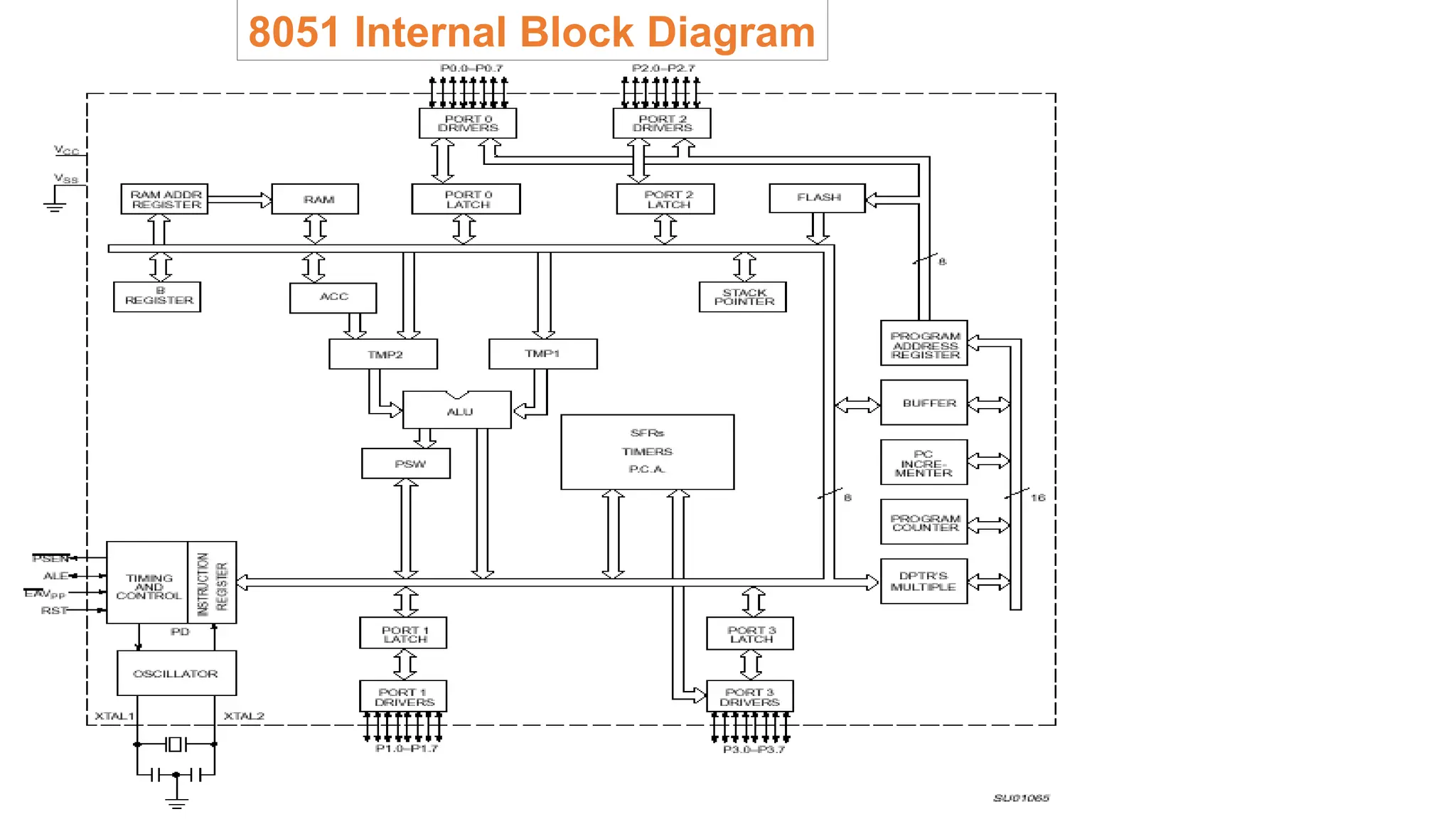
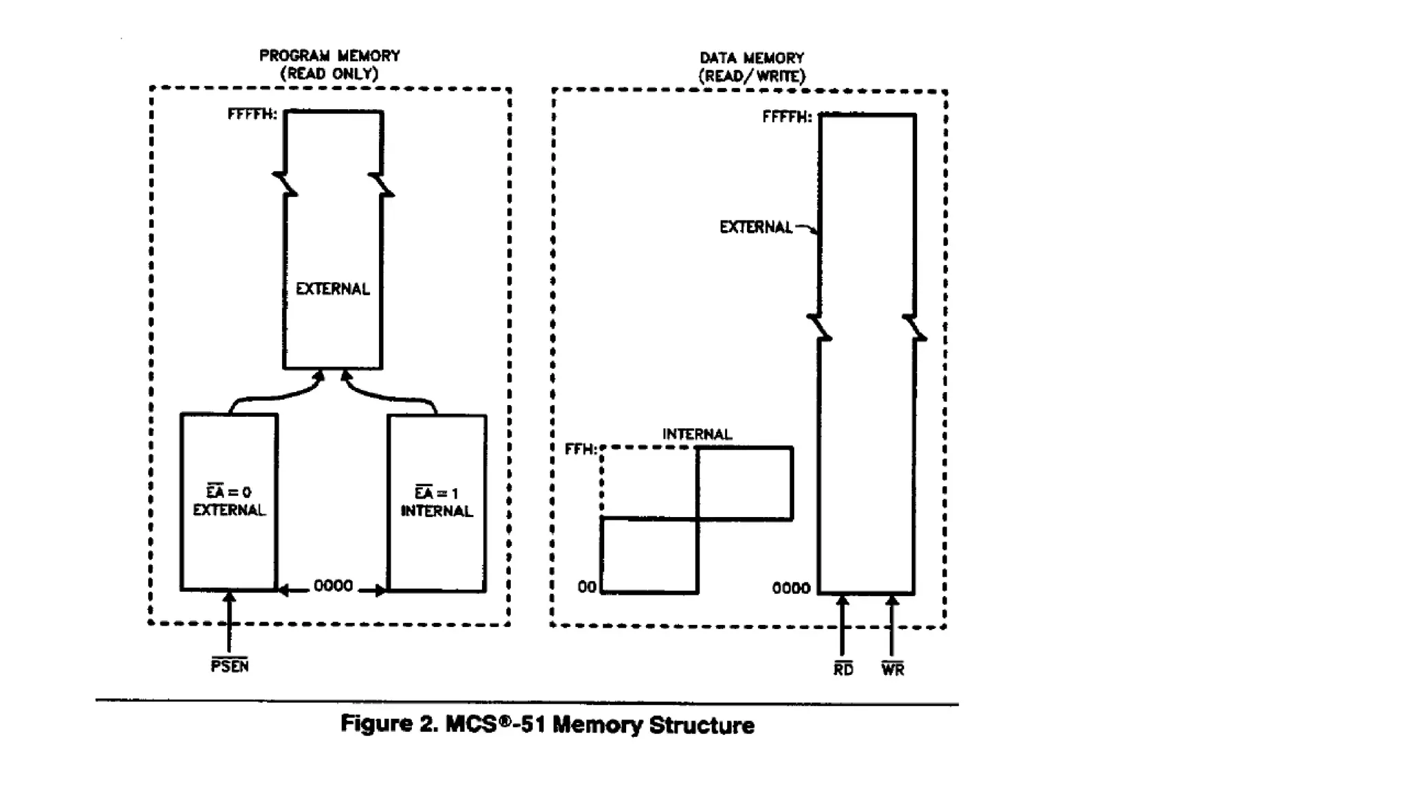
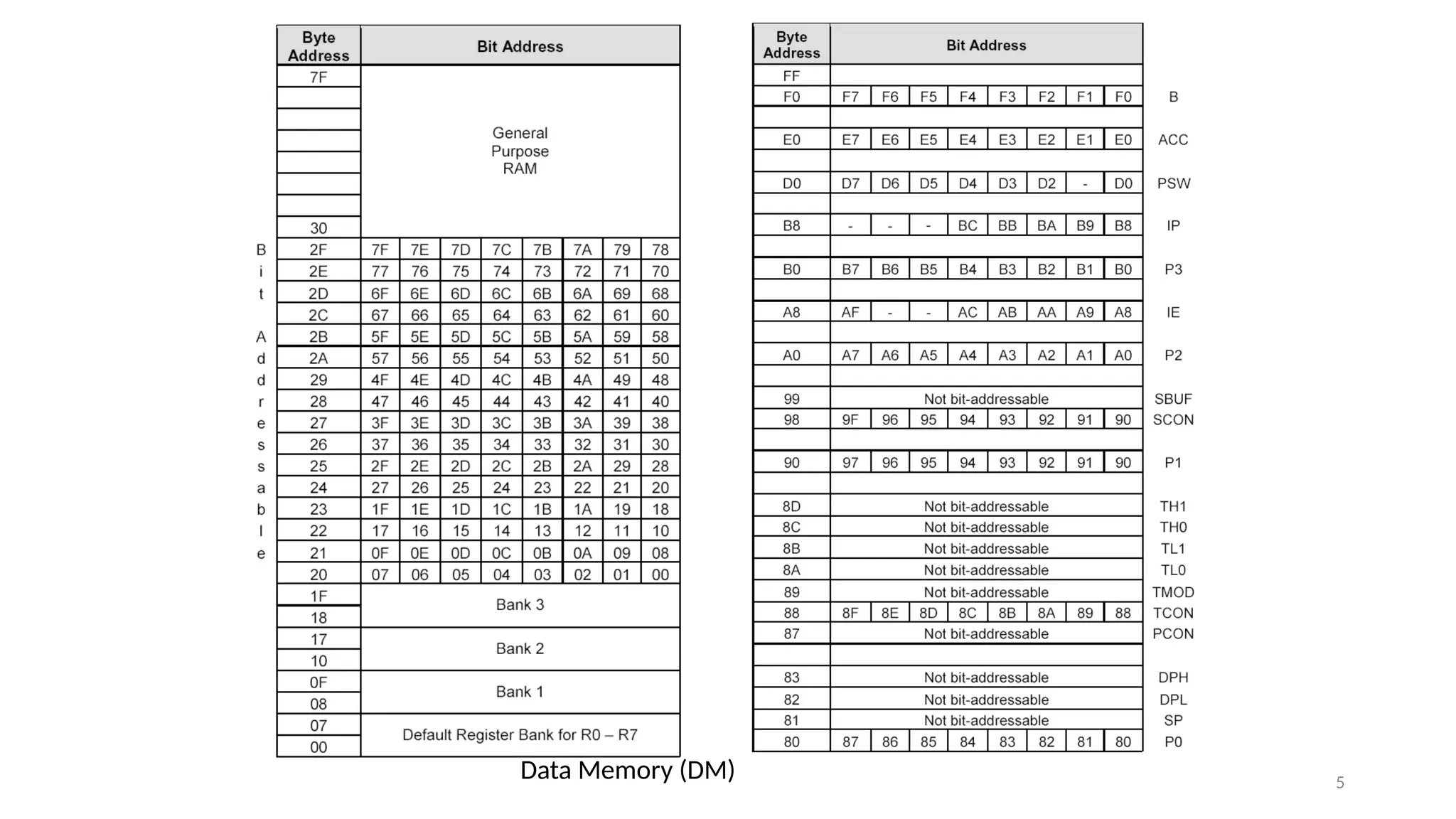
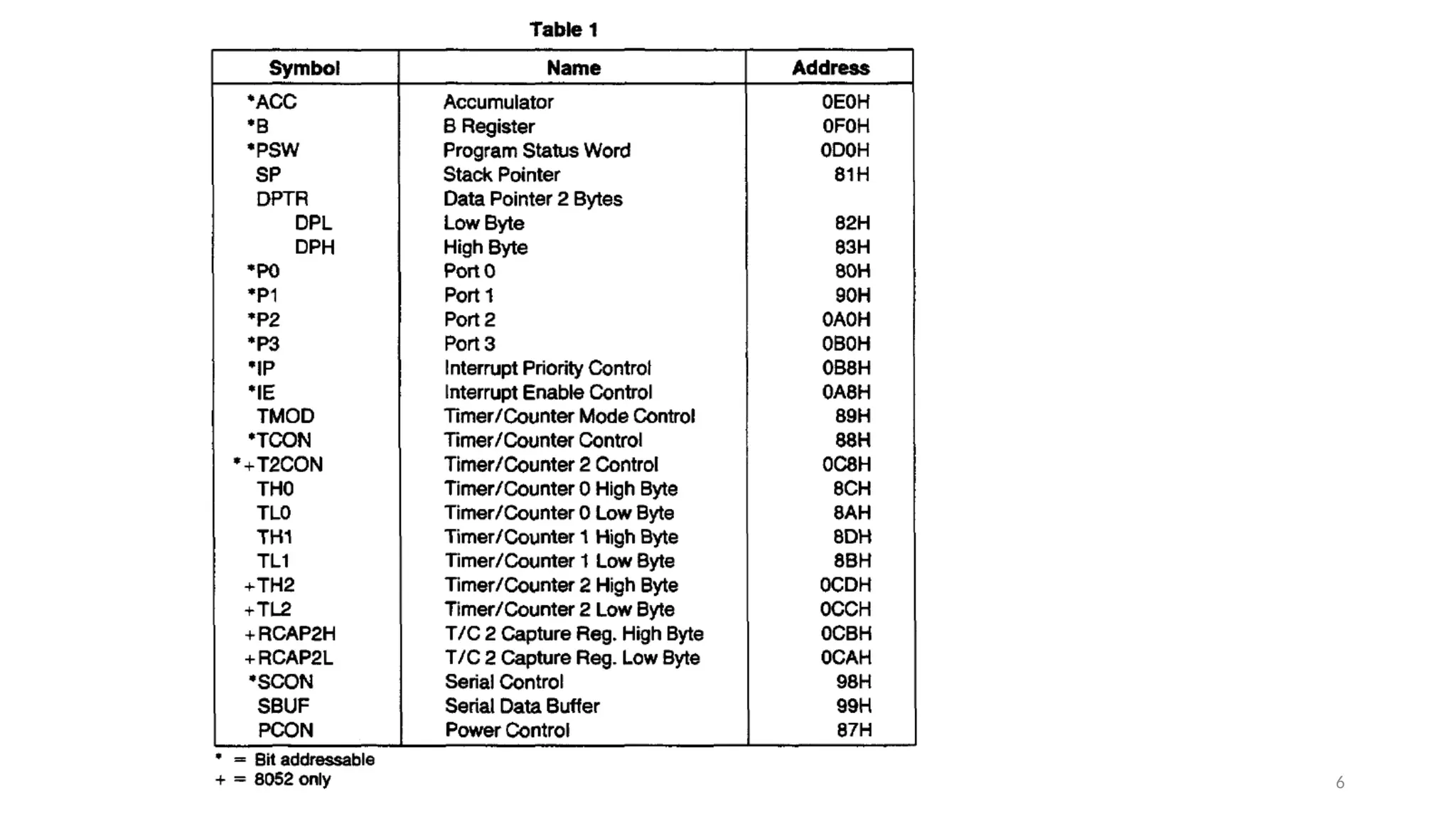
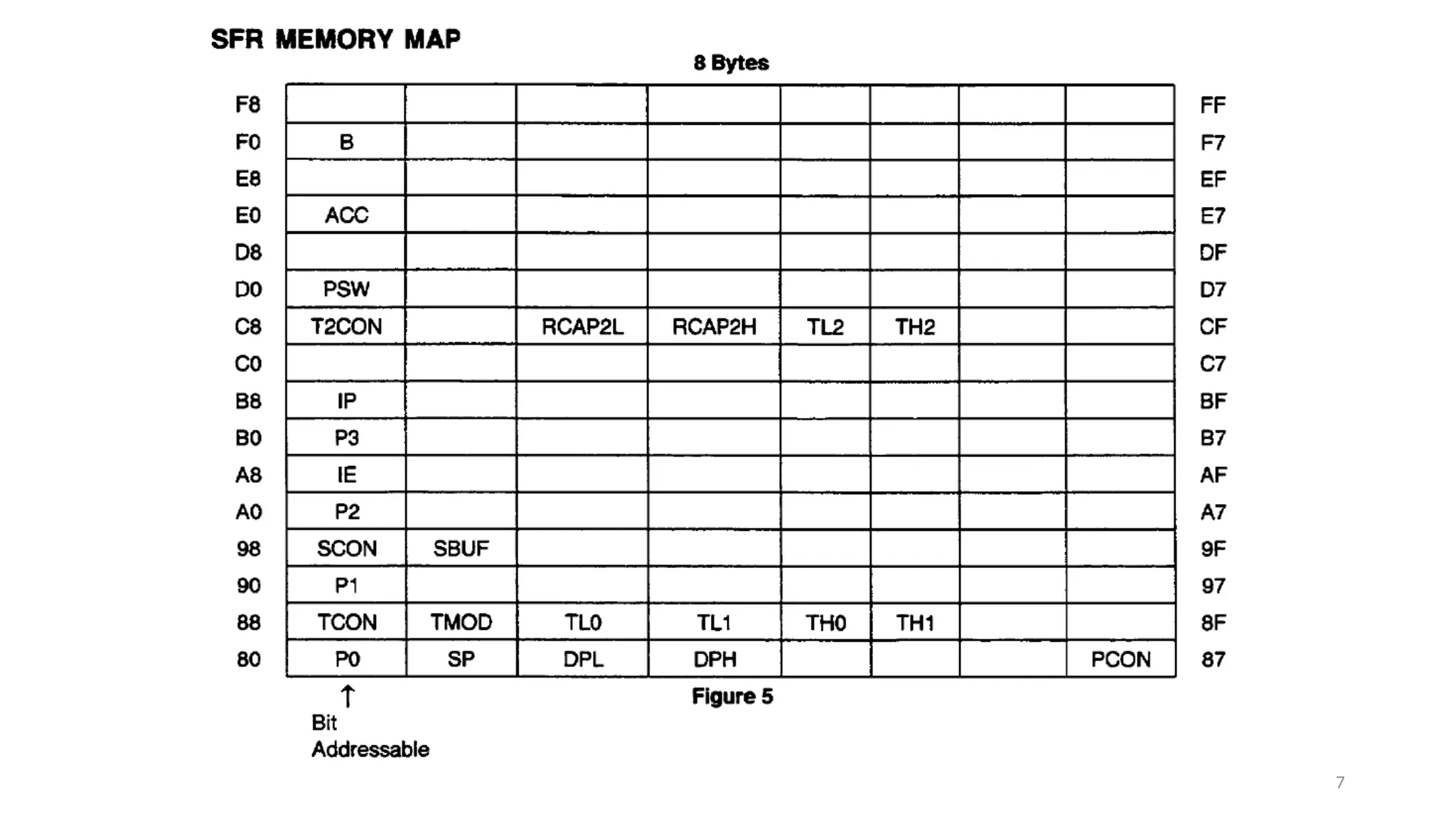
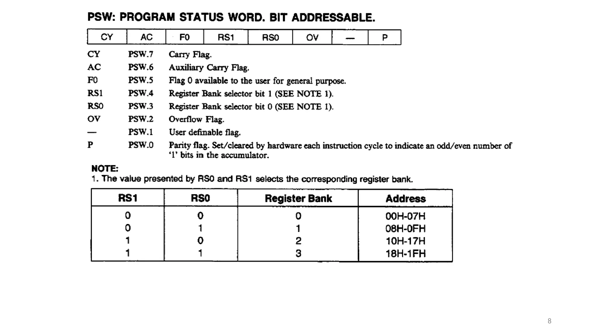
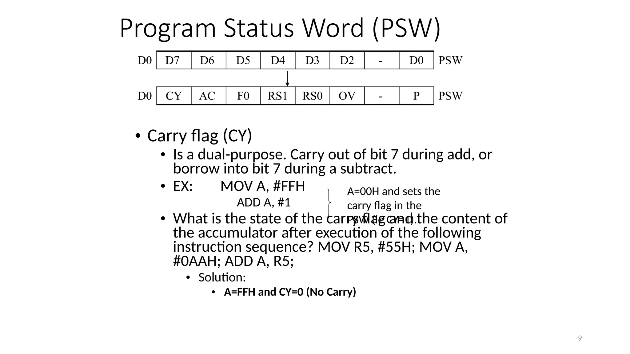
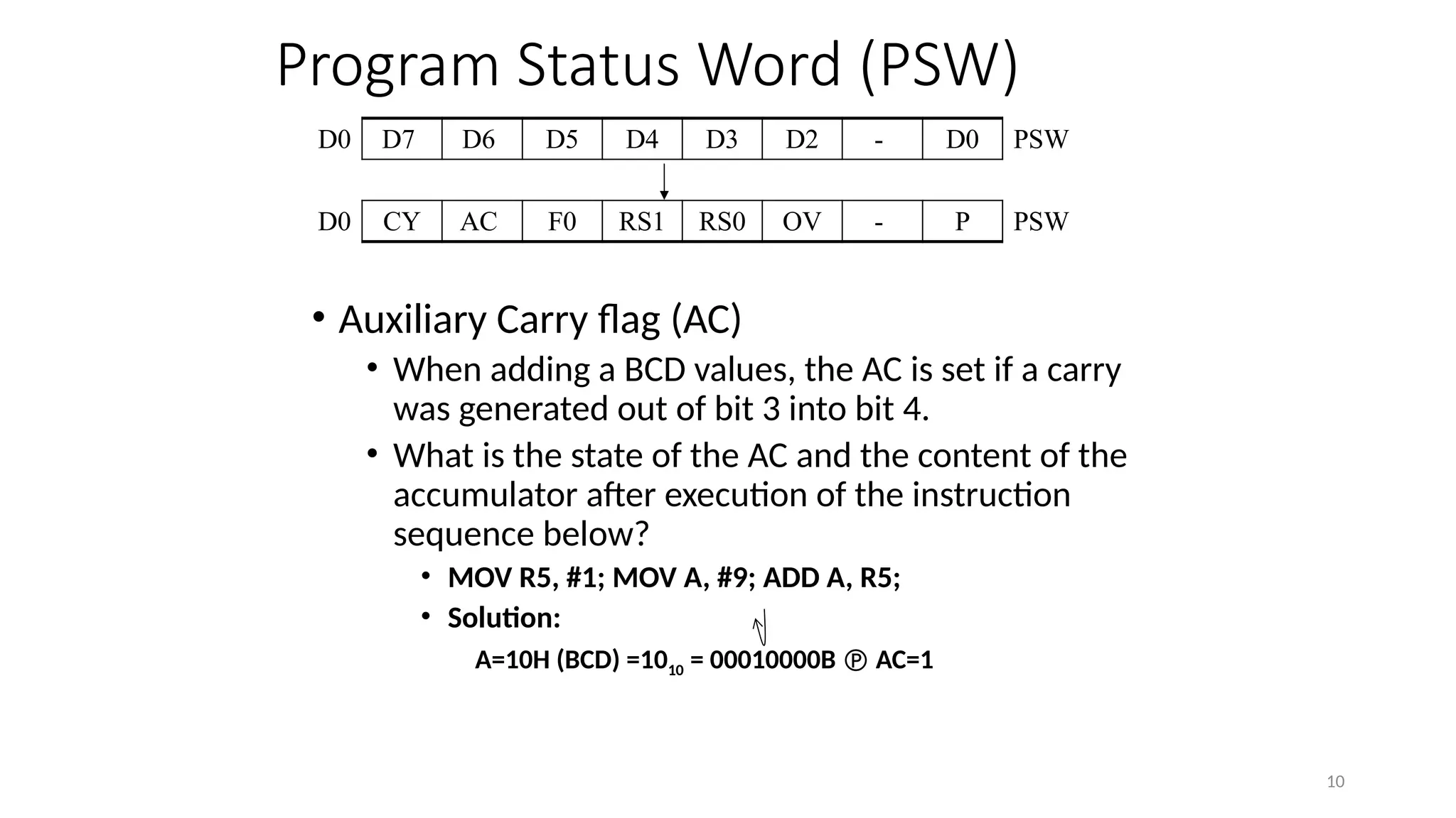
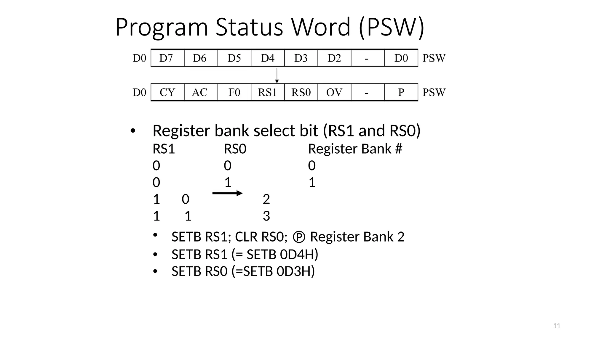
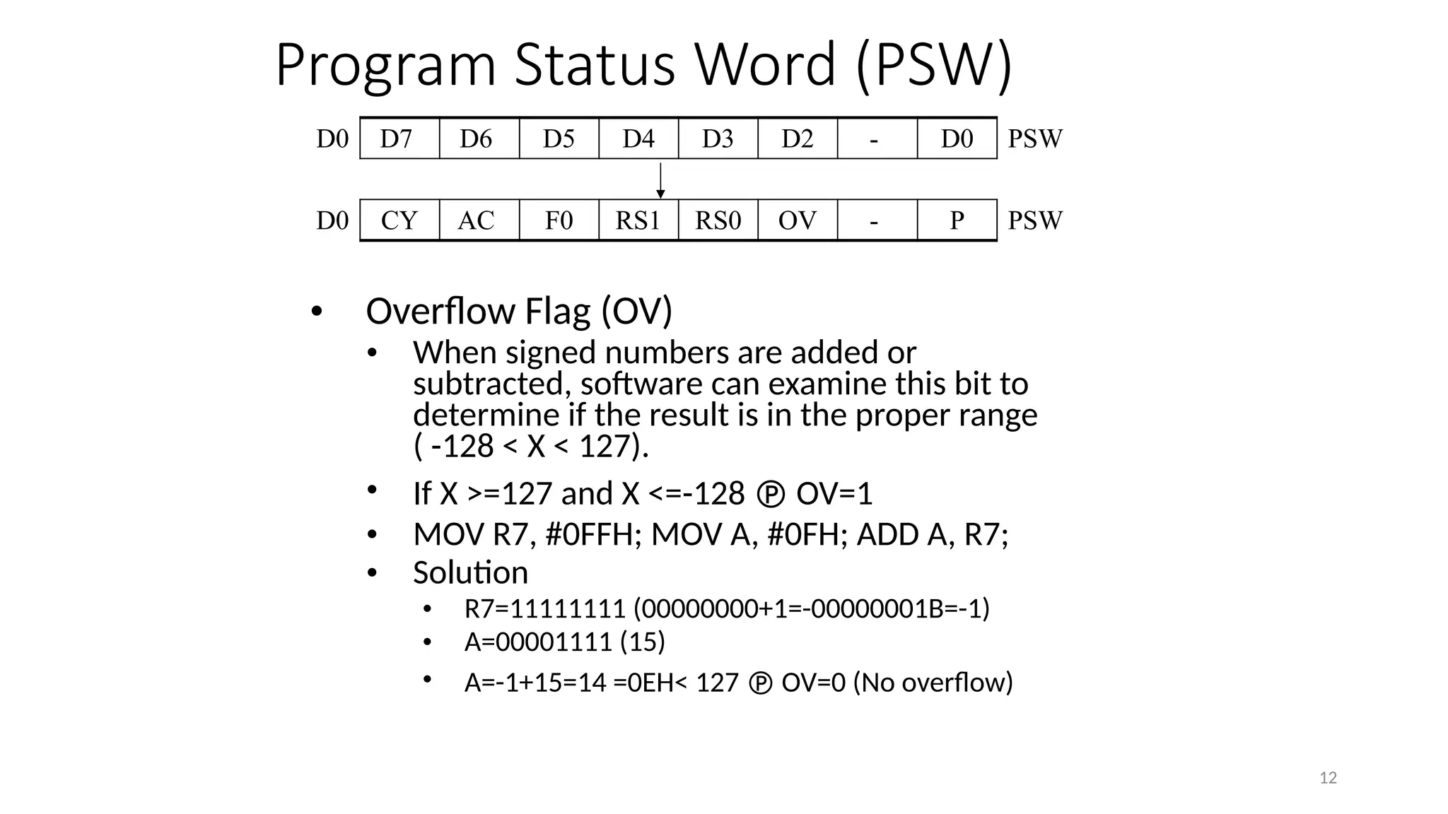
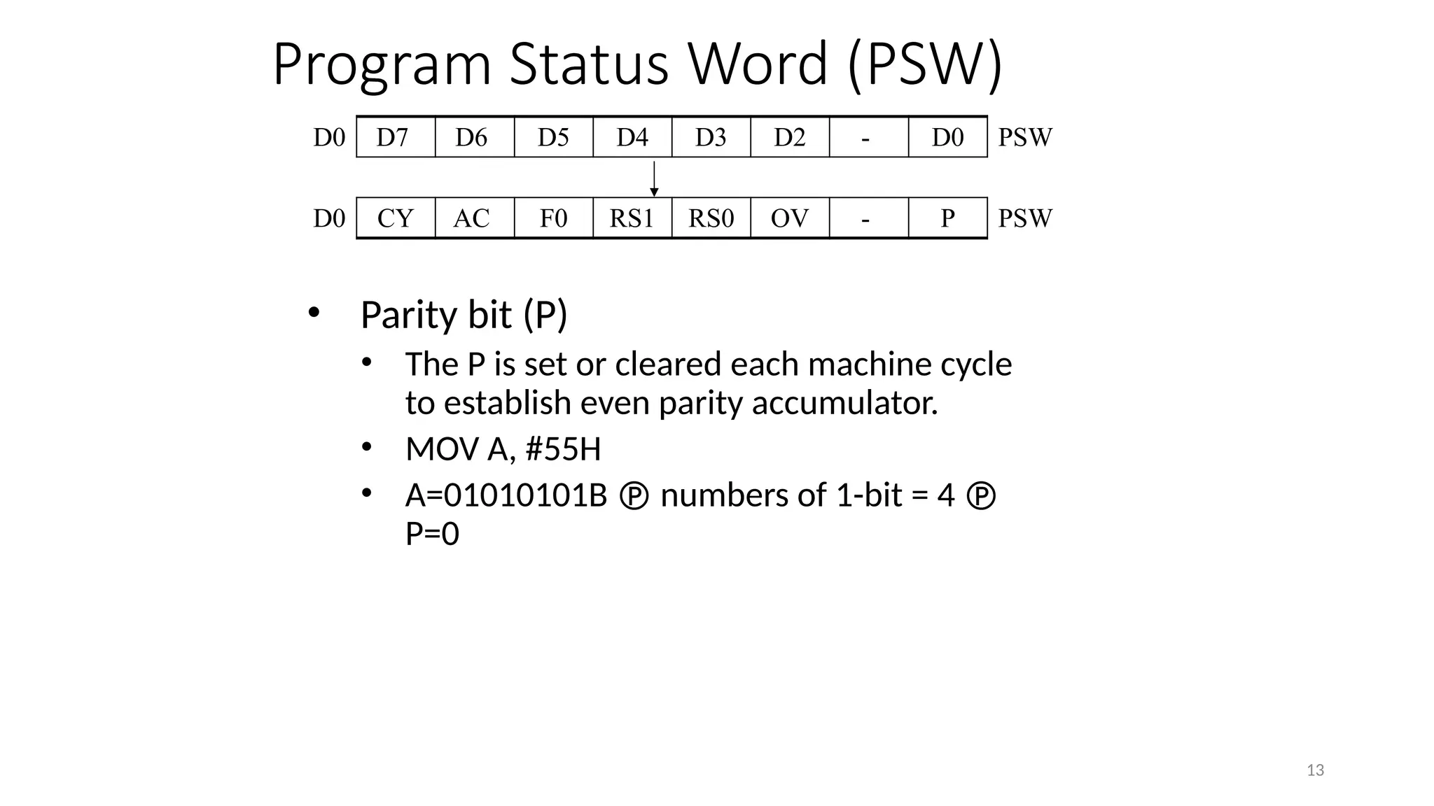
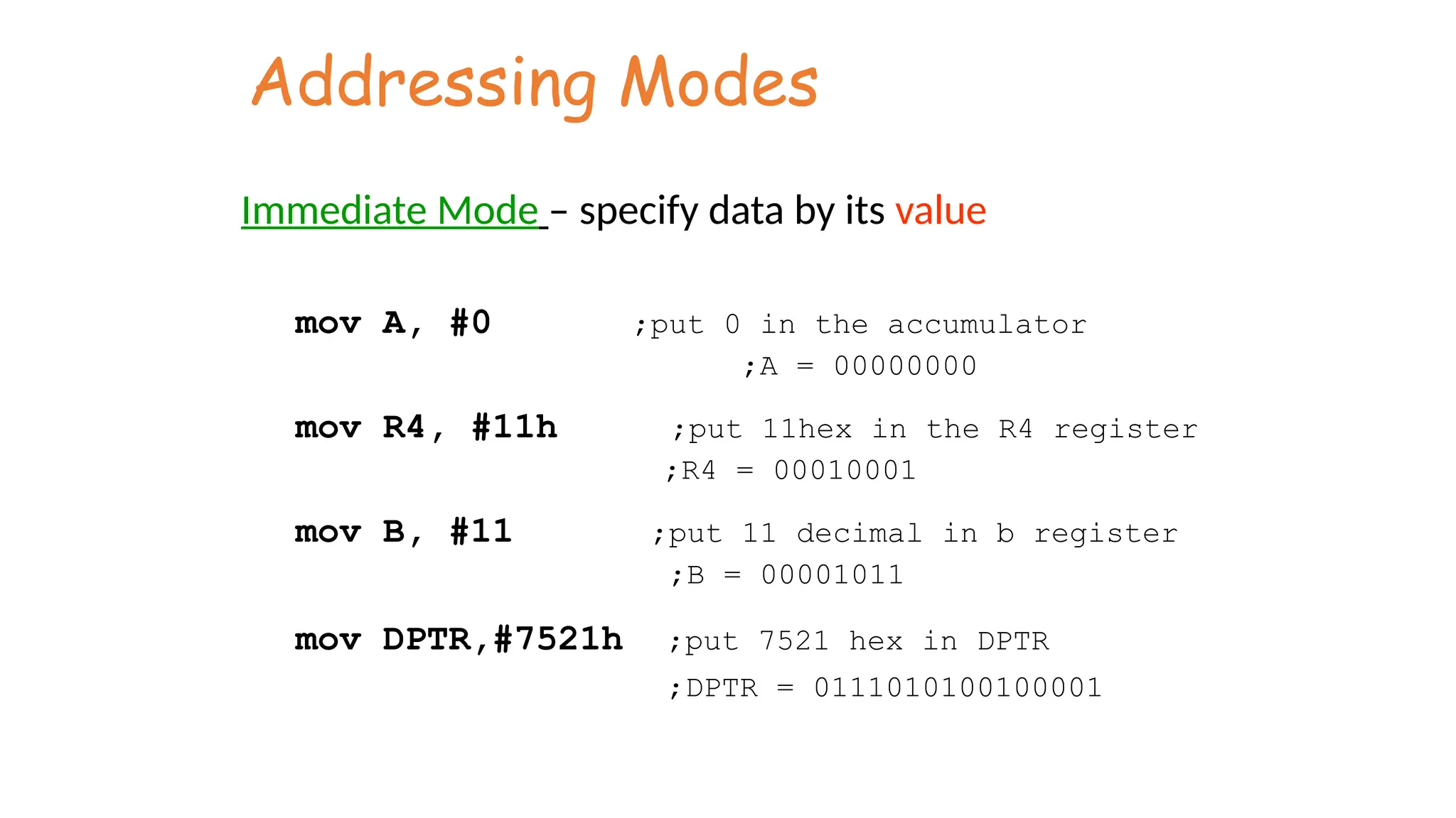
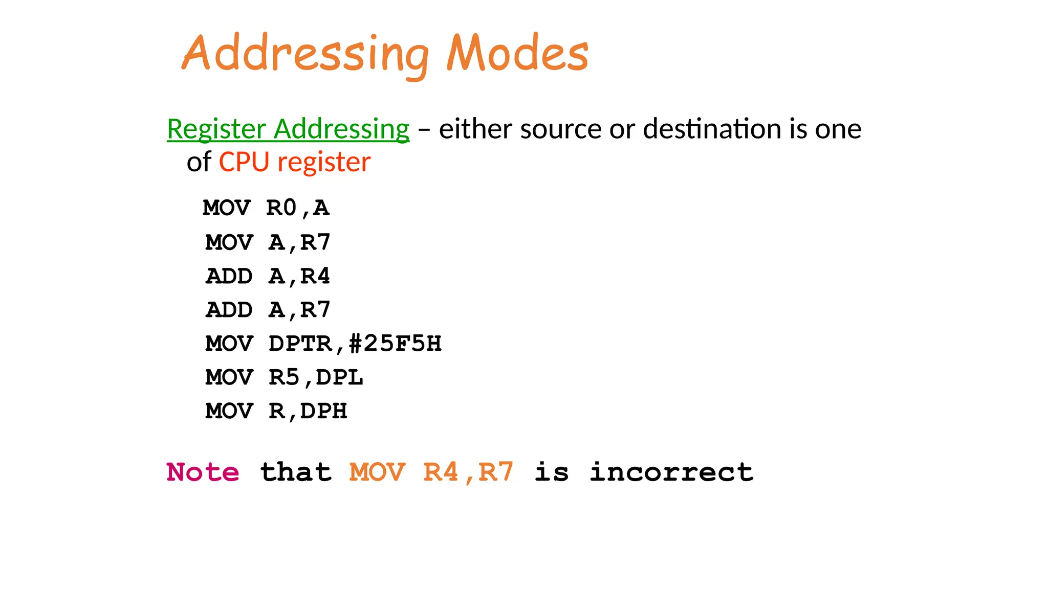
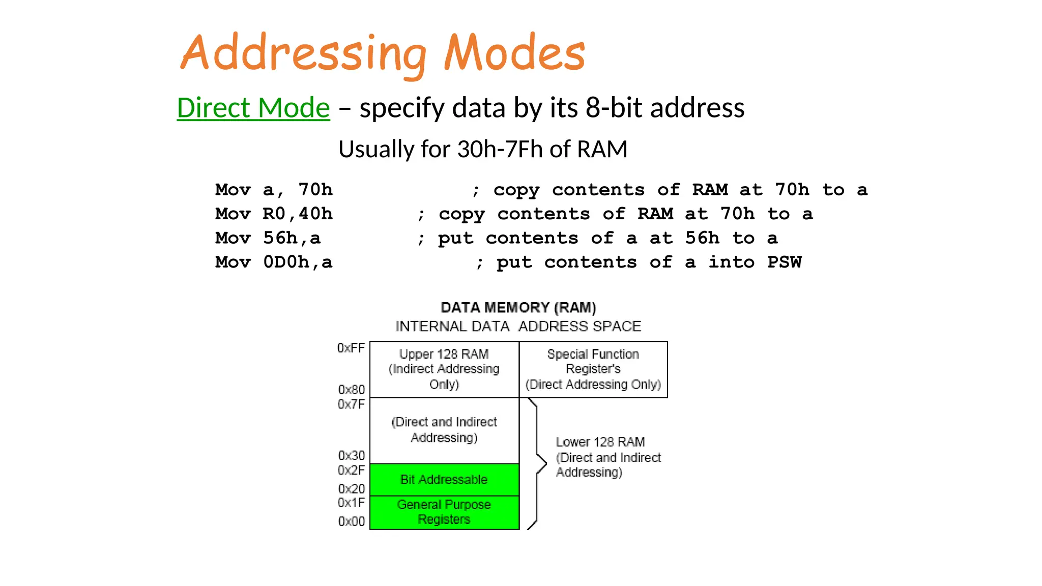
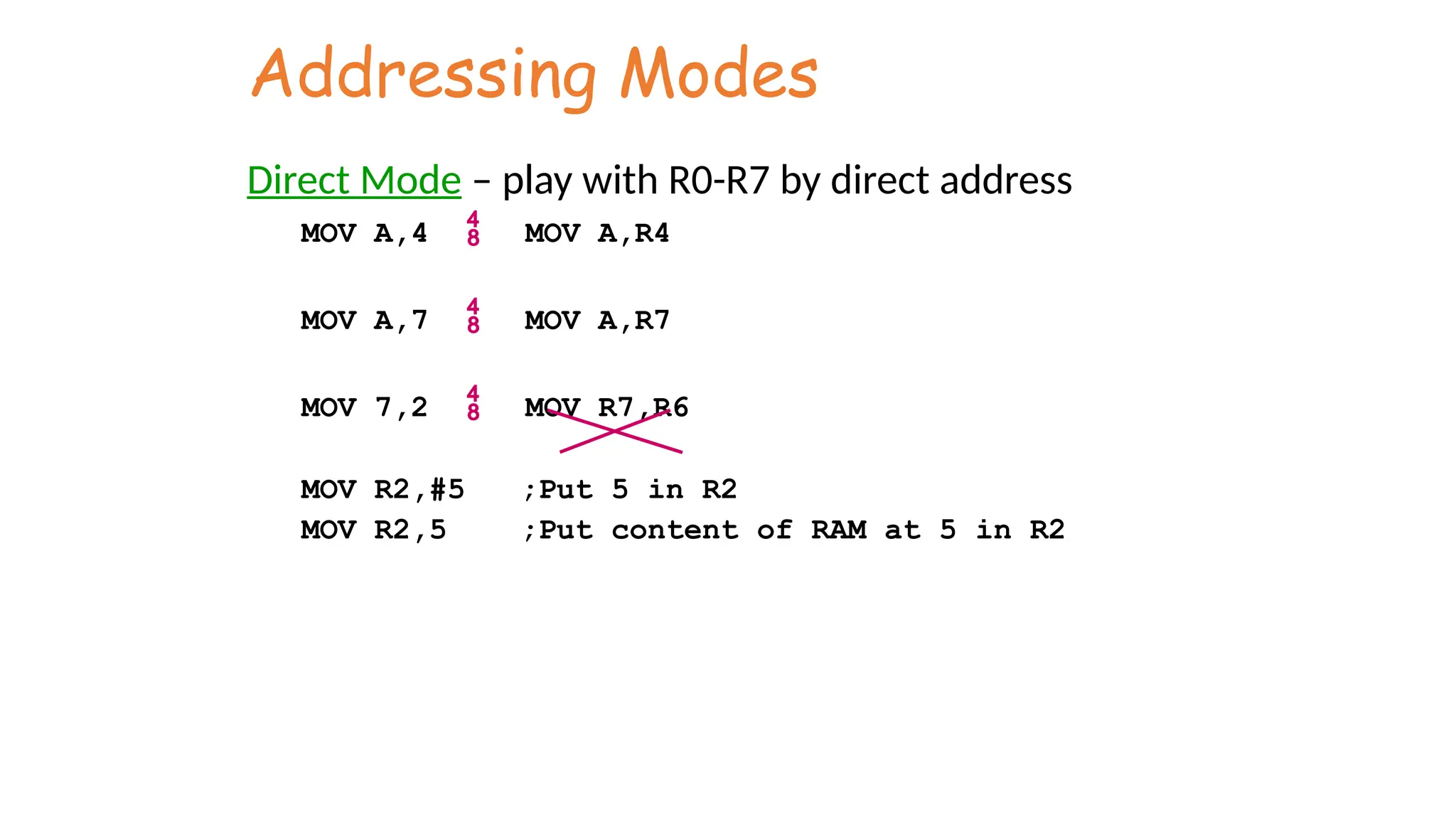
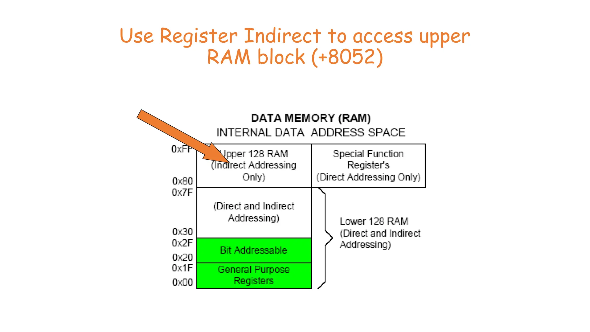
The document provides an overview of the 8051 microcontroller's internal architecture, including its instruction set, data memory operations, and program status word (PSW) flags such as the carry, auxiliary carry, overflow, and parity bits. It explains various addressing modes including immediate, register, direct, and indirect addressing, with examples for each mode. Furthermore, the document covers how the PSW can be used to determine the state of specific operations and the handling of binary-coded decimal (BCD) values.
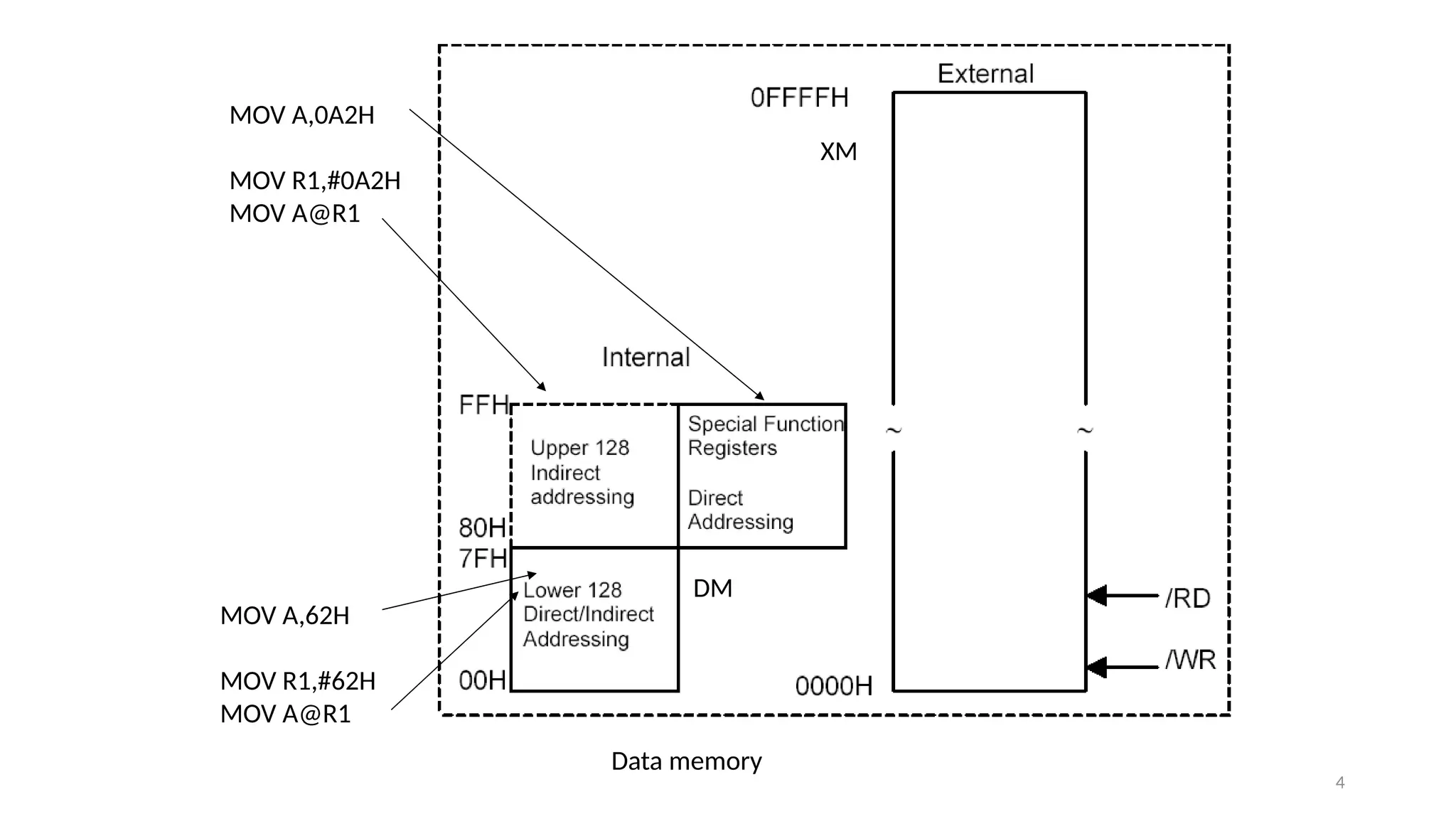
![Addressing Modes Register Indirect – the address of the source or destination is specified in registers Uses registers R0 or R1 for 8-bit address: mov psw, #0 ; use register bank 0 mov r0, #0x3C mov @r0, #3 ; memory at 3C gets #3 ; M[3C] 3 Uses DPTR register for 16-bit addresses: mov dptr, #0x9000 ; dptr 9000h movx a, @dptr ; a M[9000] Note that 9000 is an address in external memory](https://image.slidesharecdn.com/presentation1-241002235234-189593e9/75/Microcontroller-Introduction-and-the-various-features-18-2048.jpg)
![Addressing Modes Register Indexed Mode – source or destination address is the sum of the base address and the accumulator(Index) • Base address can be DPTR or PC mov dptr, #4000h mov a, #5 movc a, @a + dptr ;a M[4005]](https://image.slidesharecdn.com/presentation1-241002235234-189593e9/75/Microcontroller-Introduction-and-the-various-features-20-2048.jpg)
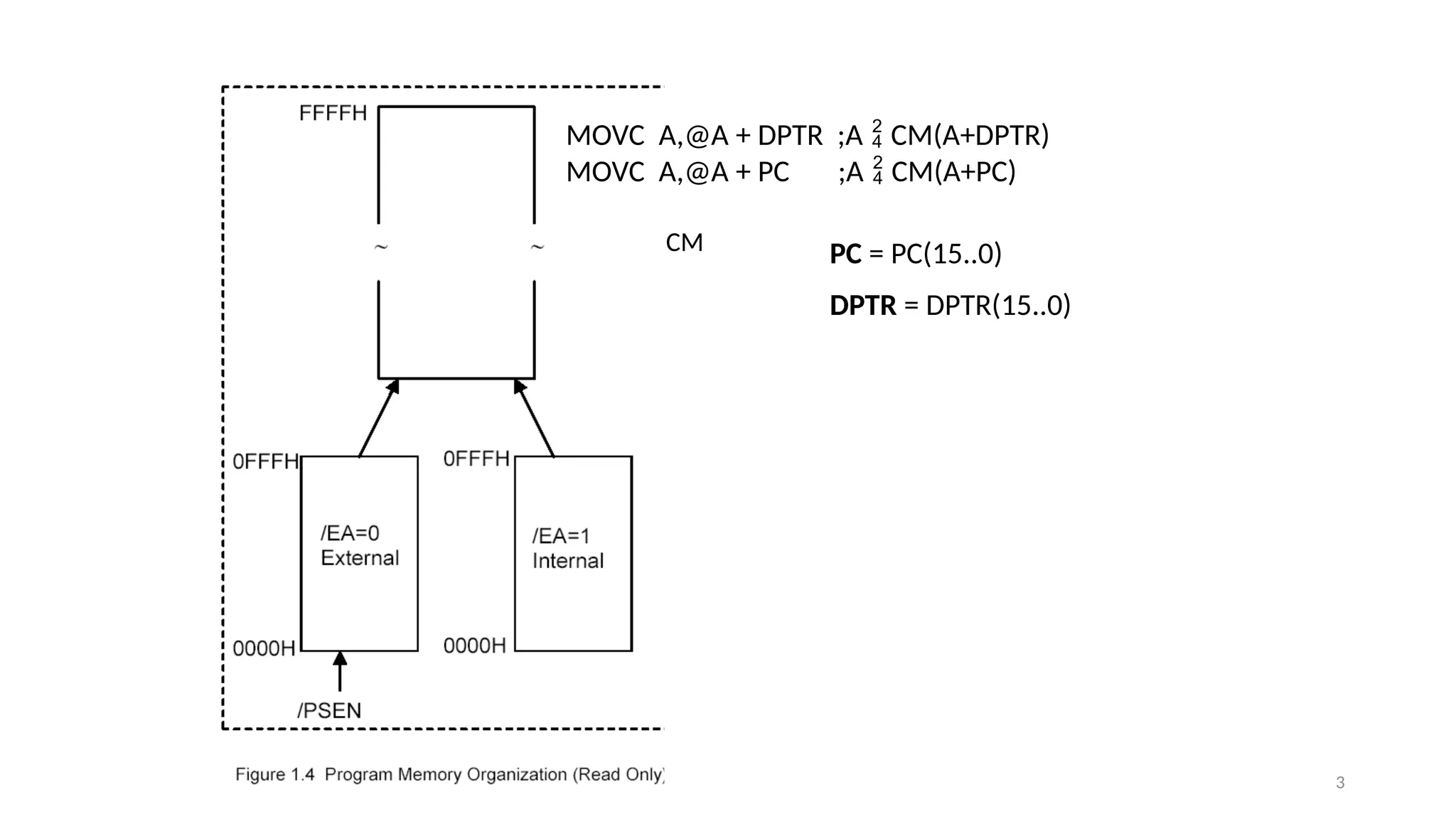
![Addressing Modes Register Indexed Mode continue • Base address can be DPTR or PC ORG 1000h 1000 mov a, #5 1002 movc a, @a + PC ;a M[1008] 1003 Nop • Table Lookup • MOVC only can read internal code memory PC](https://image.slidesharecdn.com/presentation1-241002235234-189593e9/75/Microcontroller-Introduction-and-the-various-features-21-2048.jpg)