Downloaded 444 times


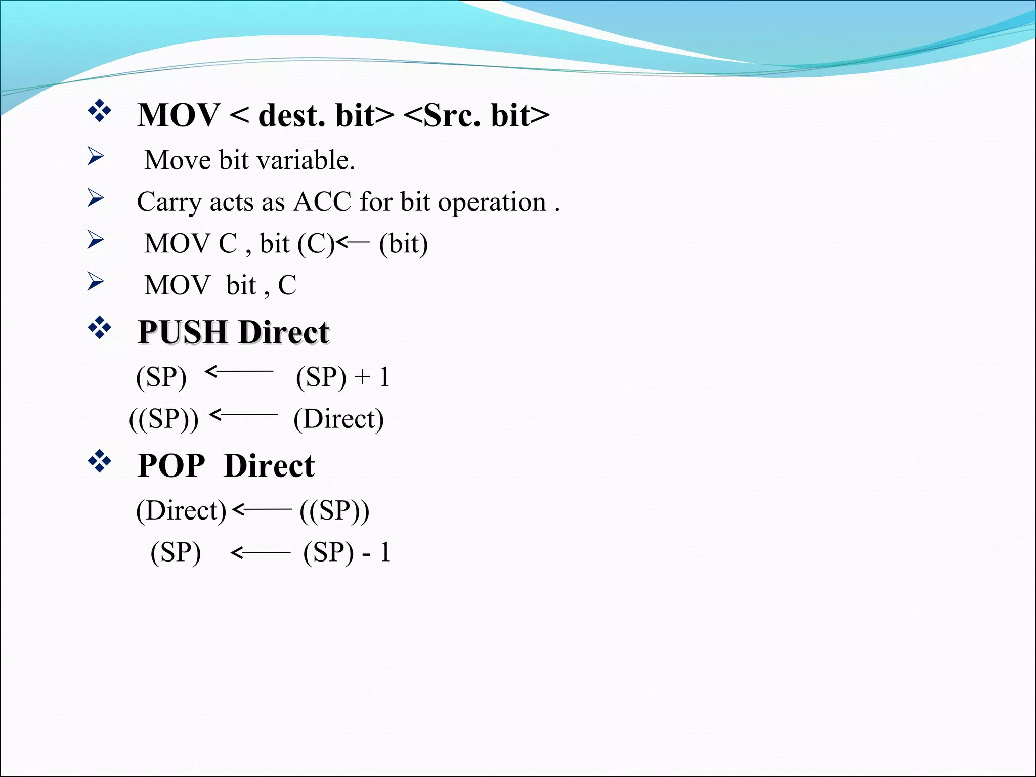
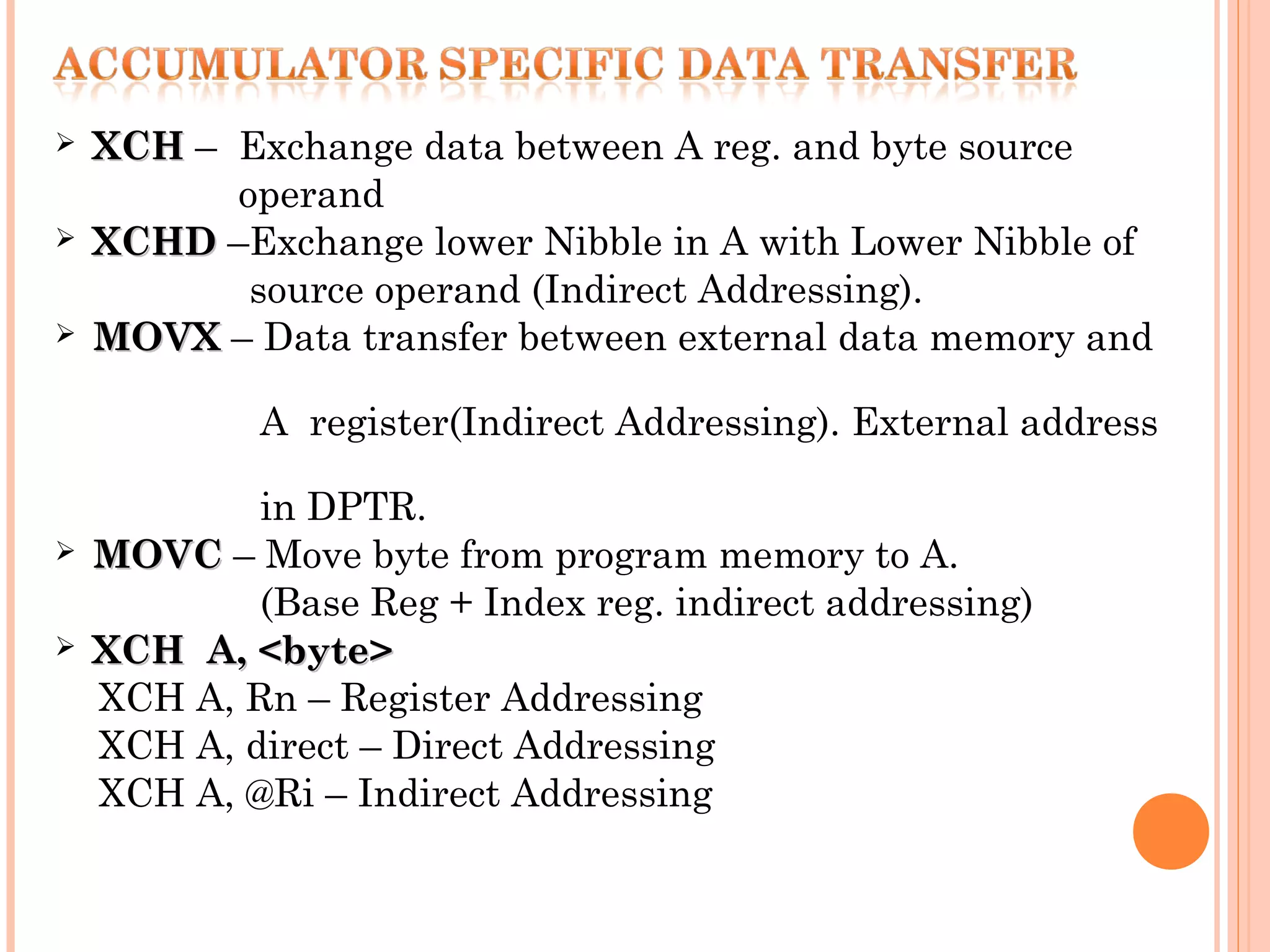
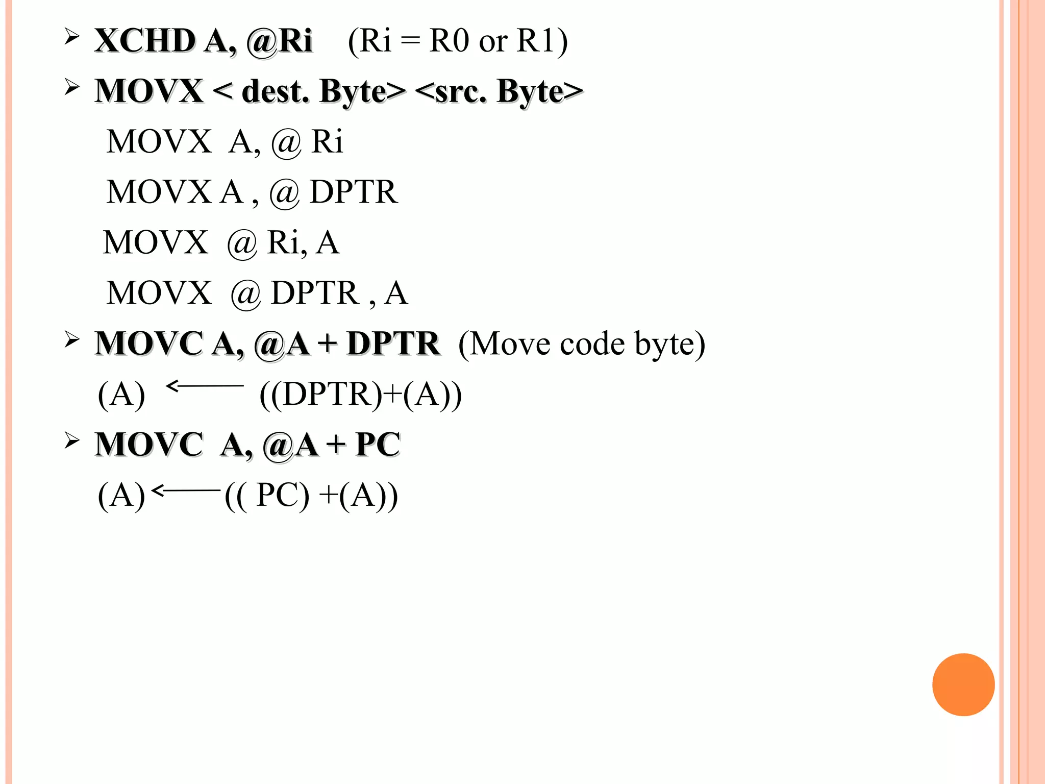
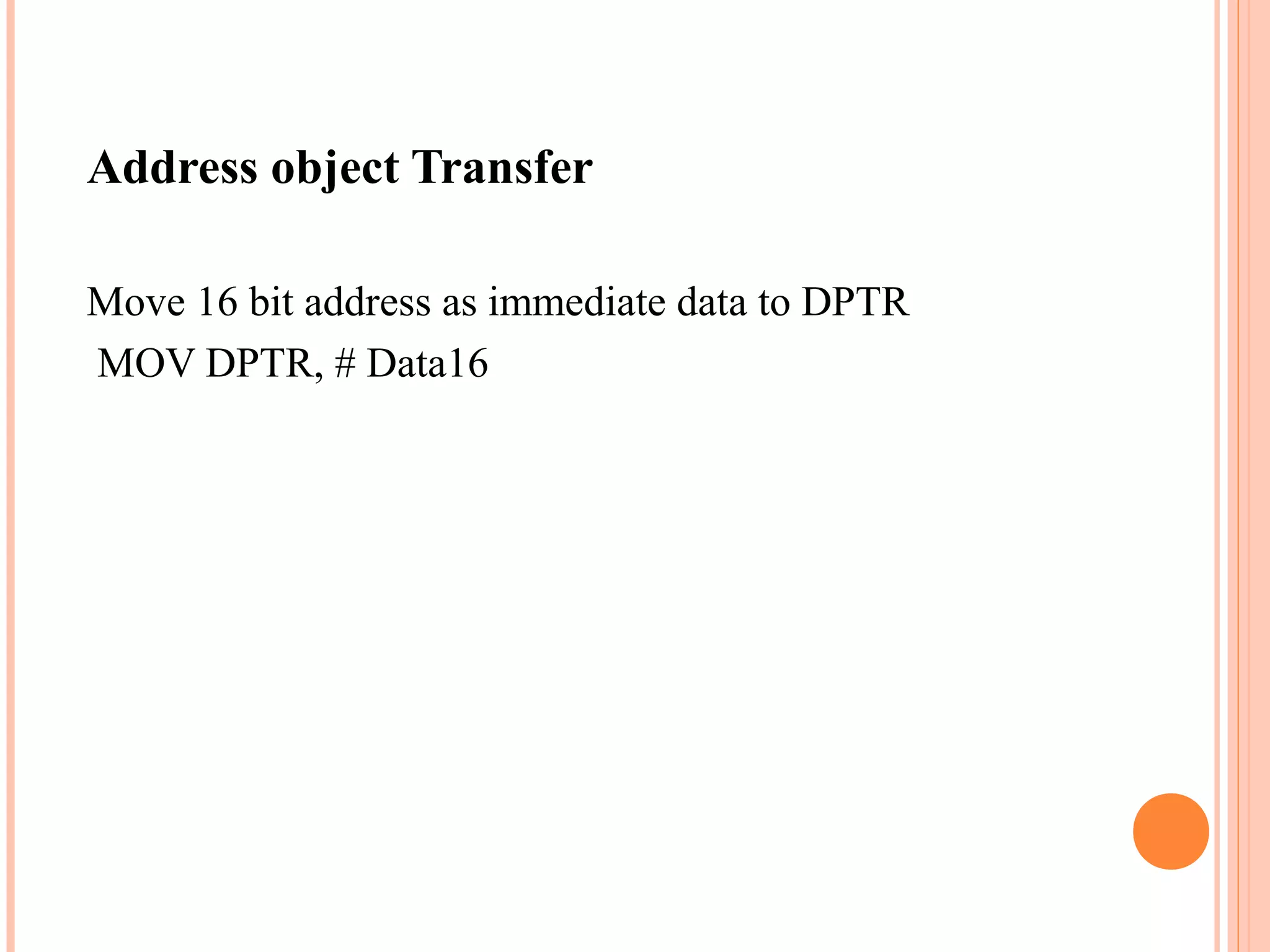


The document describes the architecture and instruction set of the 8051 microcontroller. It includes details about the memory map, internal data memory organization, special function registers, addressing modes, and common instructions. The 8051 has 4KB of on-chip ROM, 128 bytes of internal RAM, 21 special function registers, and supports operations on bytes, bits, and 16-bit data using various addressing modes like register, direct, indirect, and immediate addressing. Instructions allow data transfer, arithmetic, logic, and program control operations.
Overview of fundamental concepts including Programmer's Model, Addressing Modes, and Instruction Set.
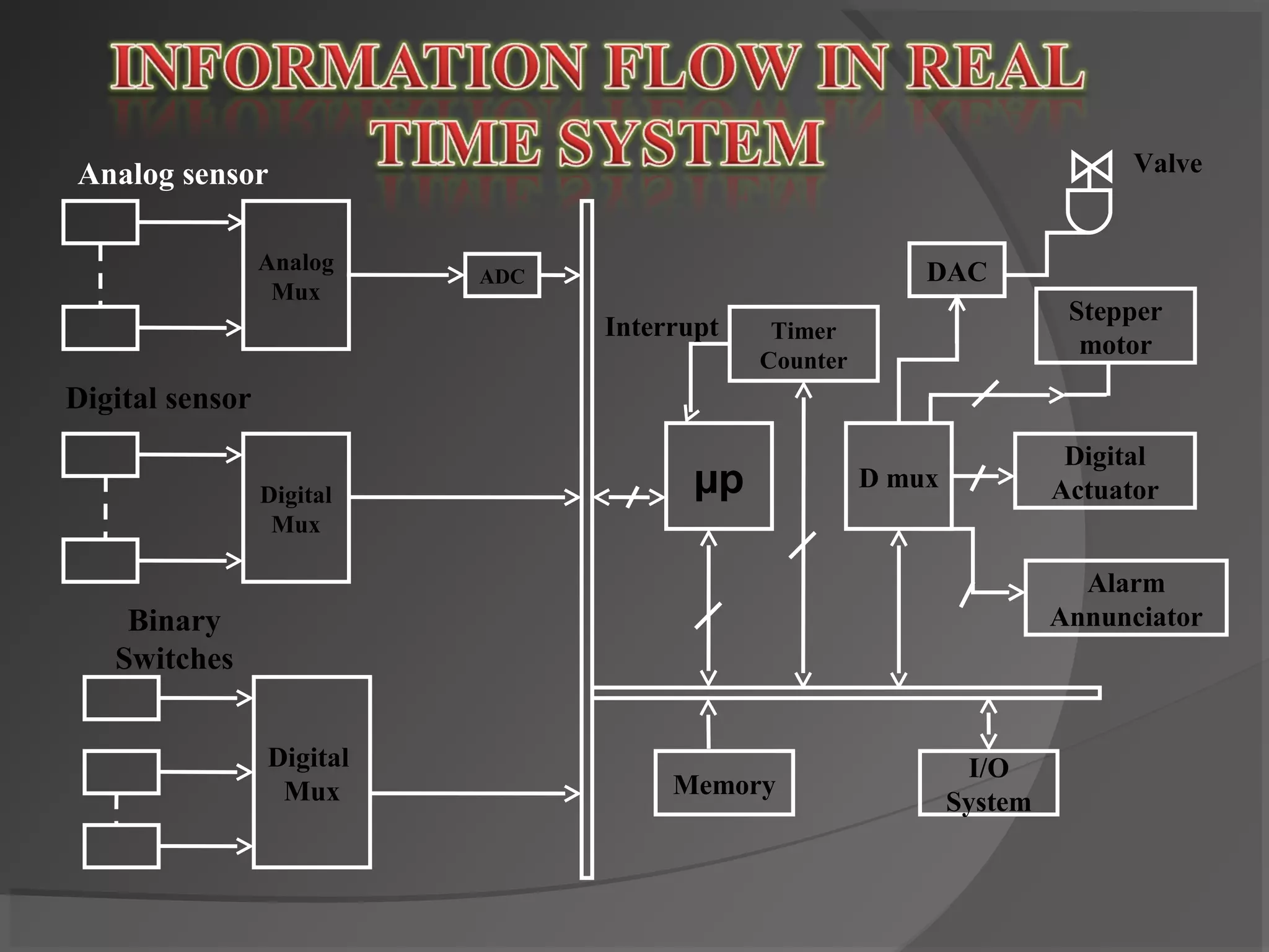
Illustration of various components including sensors (analog & digital), microcontroller (µp), and actuators.
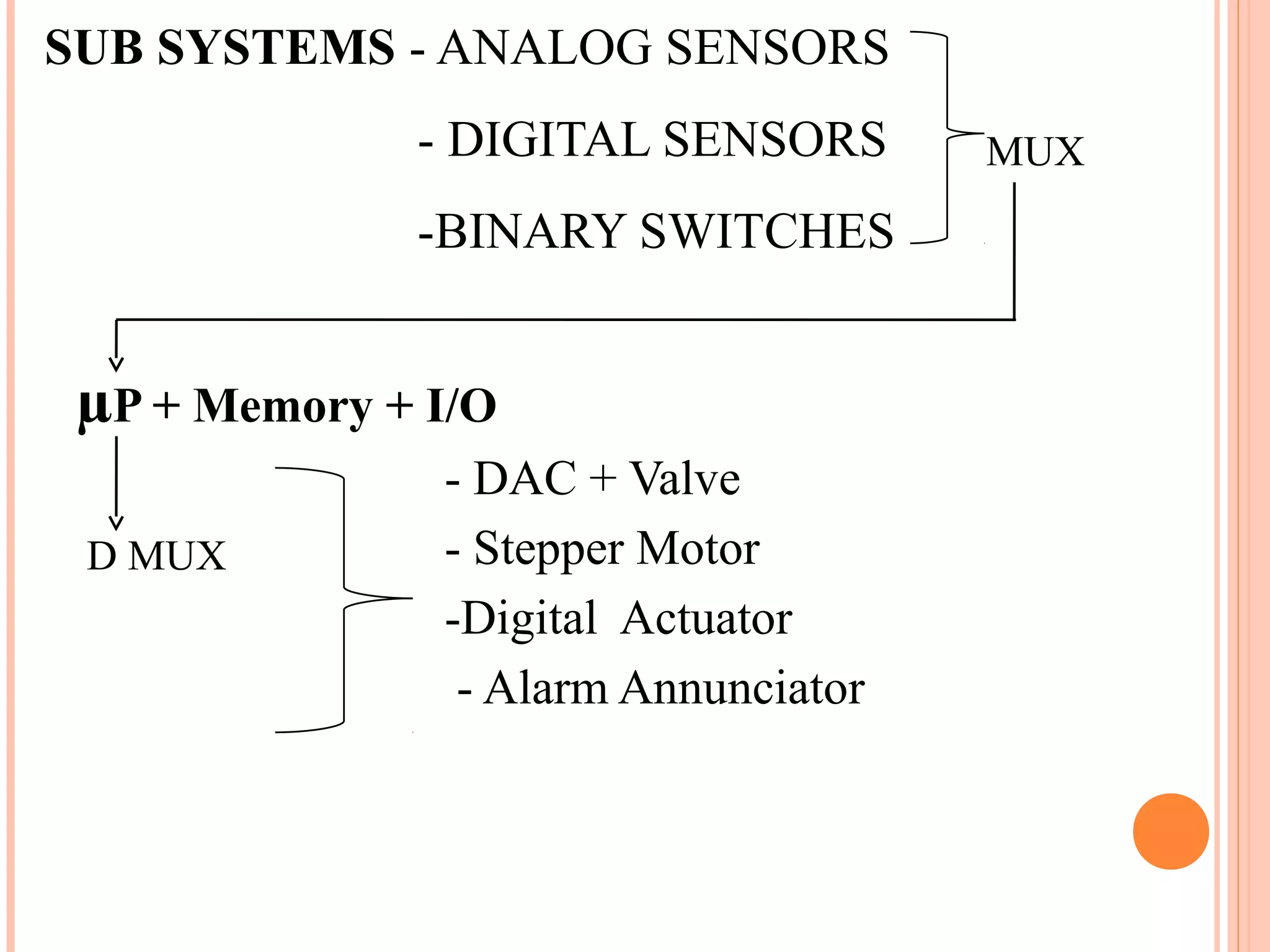
Description of subsystems focused on analog sensors, digital sensors, binary switches, and actuators.
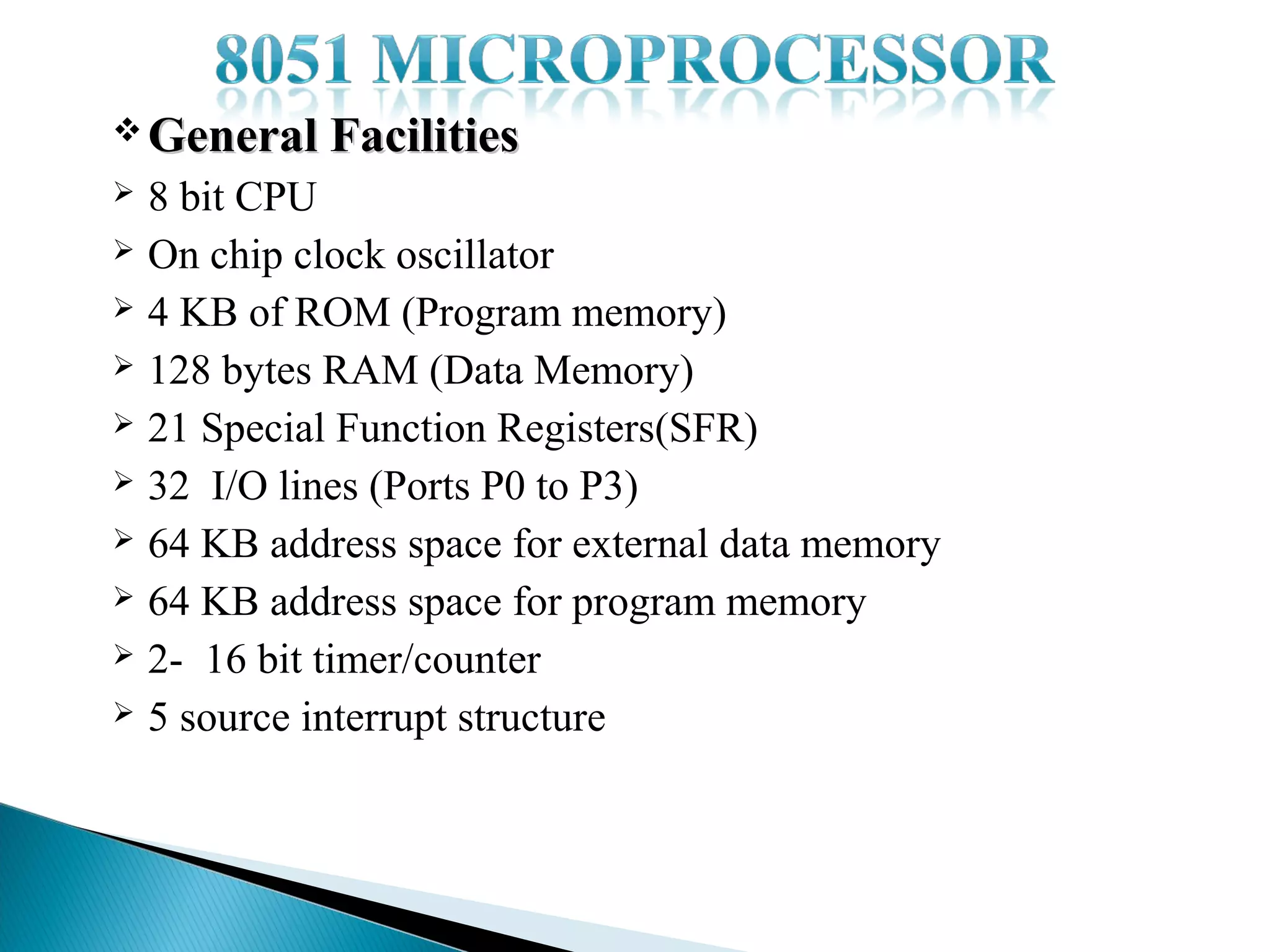
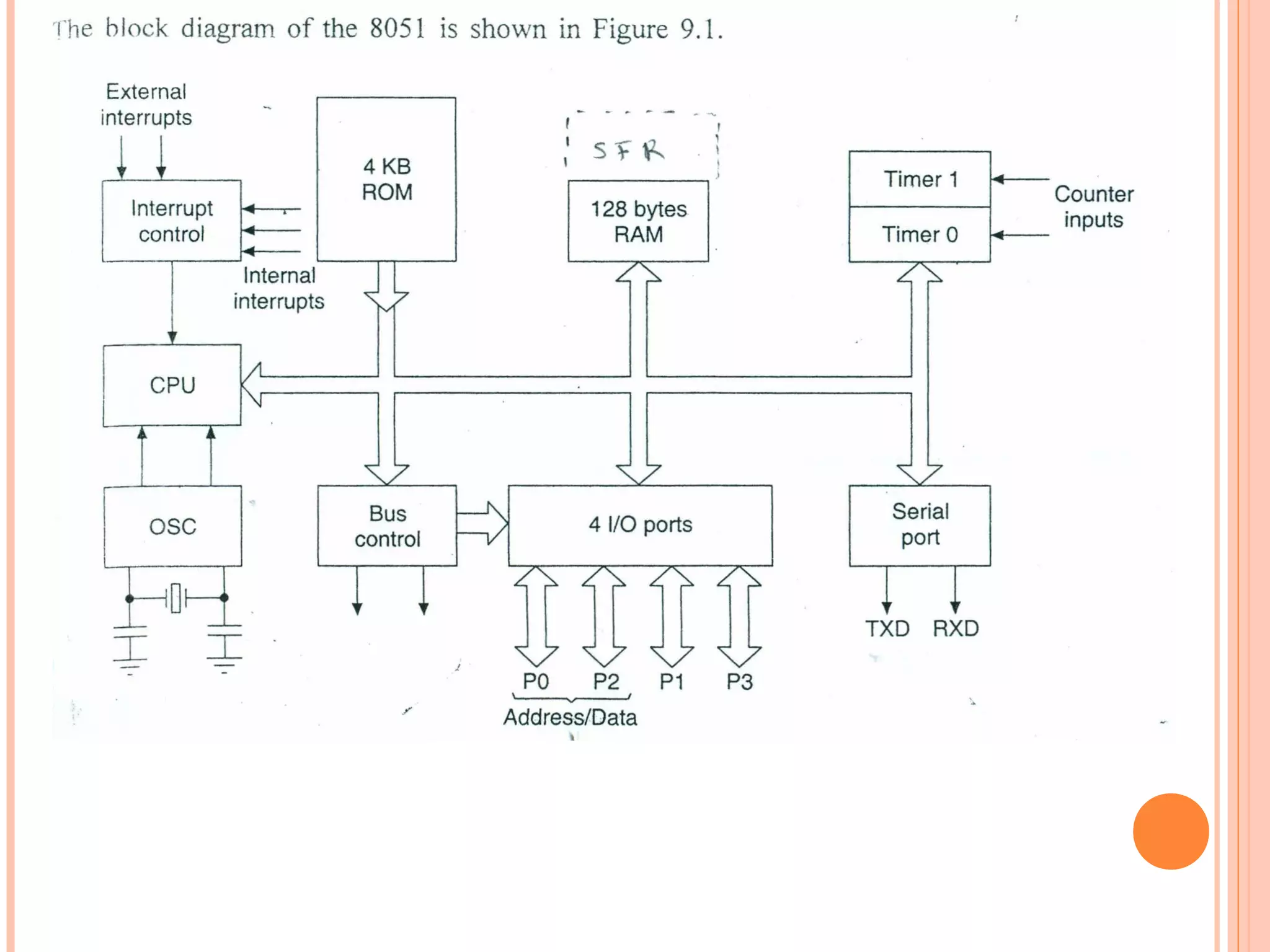
Details on CPU specifications: 8-bit CPU, ROM, RAM, I/O lines, timer/counters, interrupts.
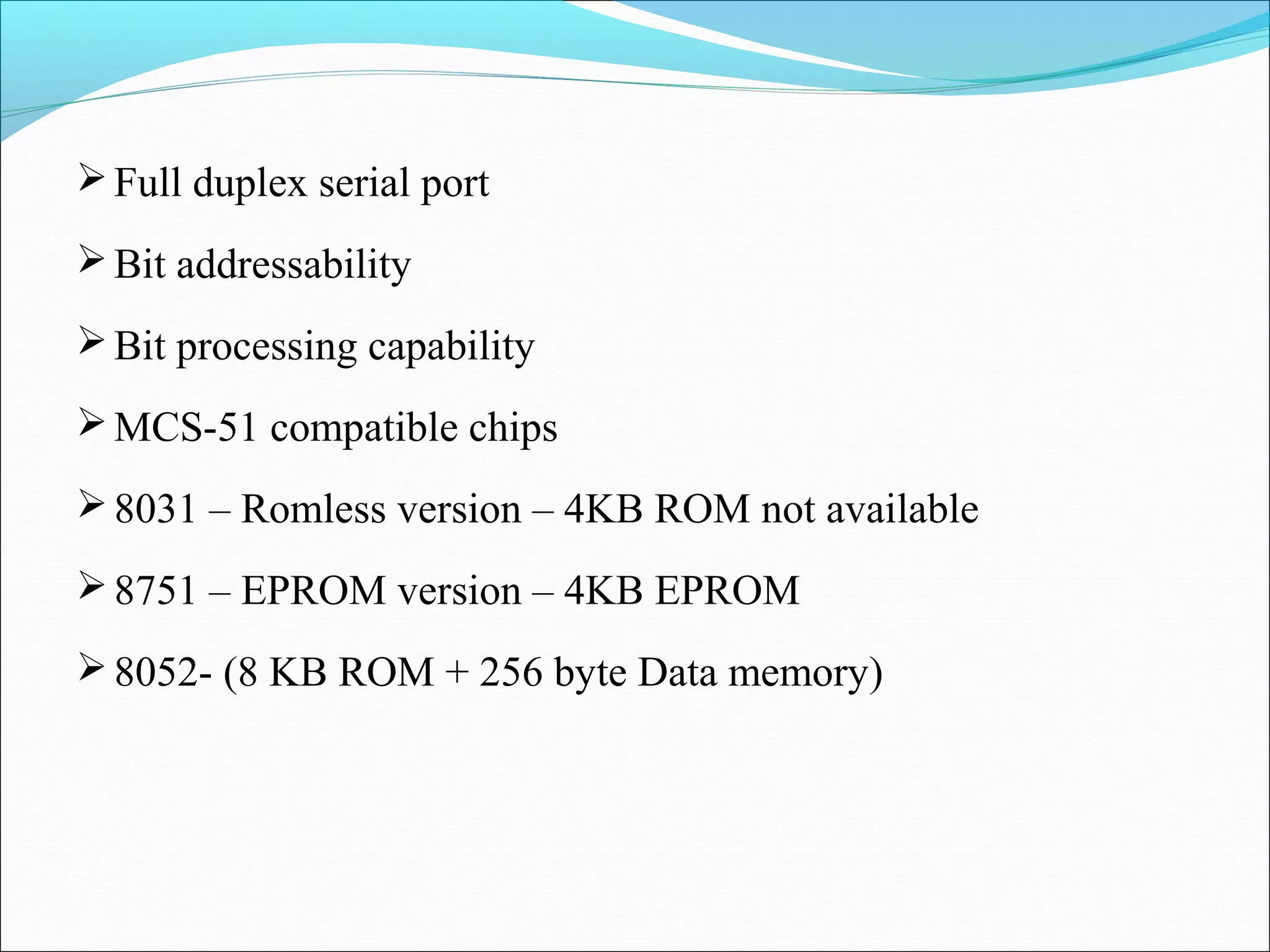
Additional CPU functionalities including full duplex serial port and compatibility with MCS-51 chips.
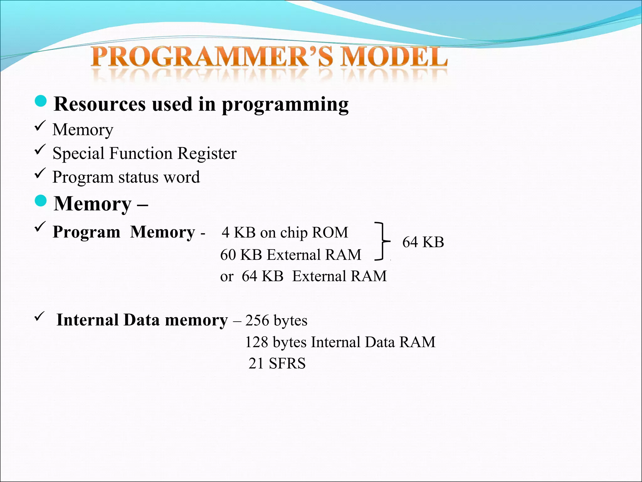
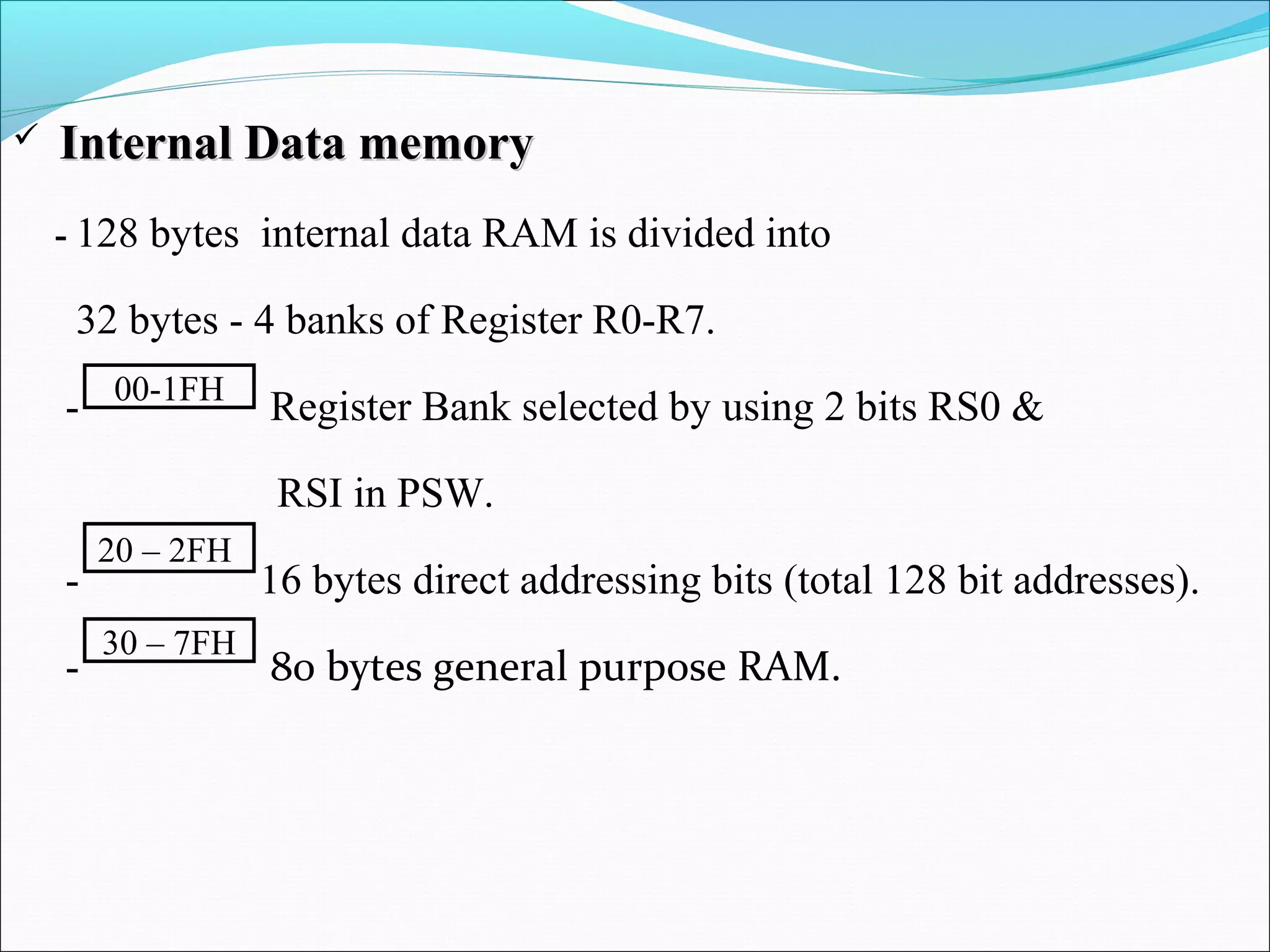
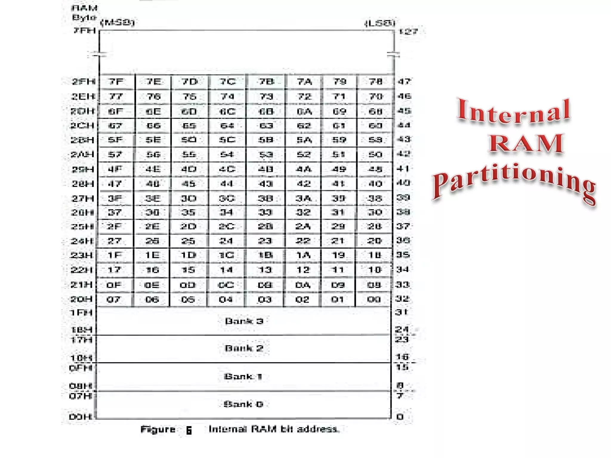
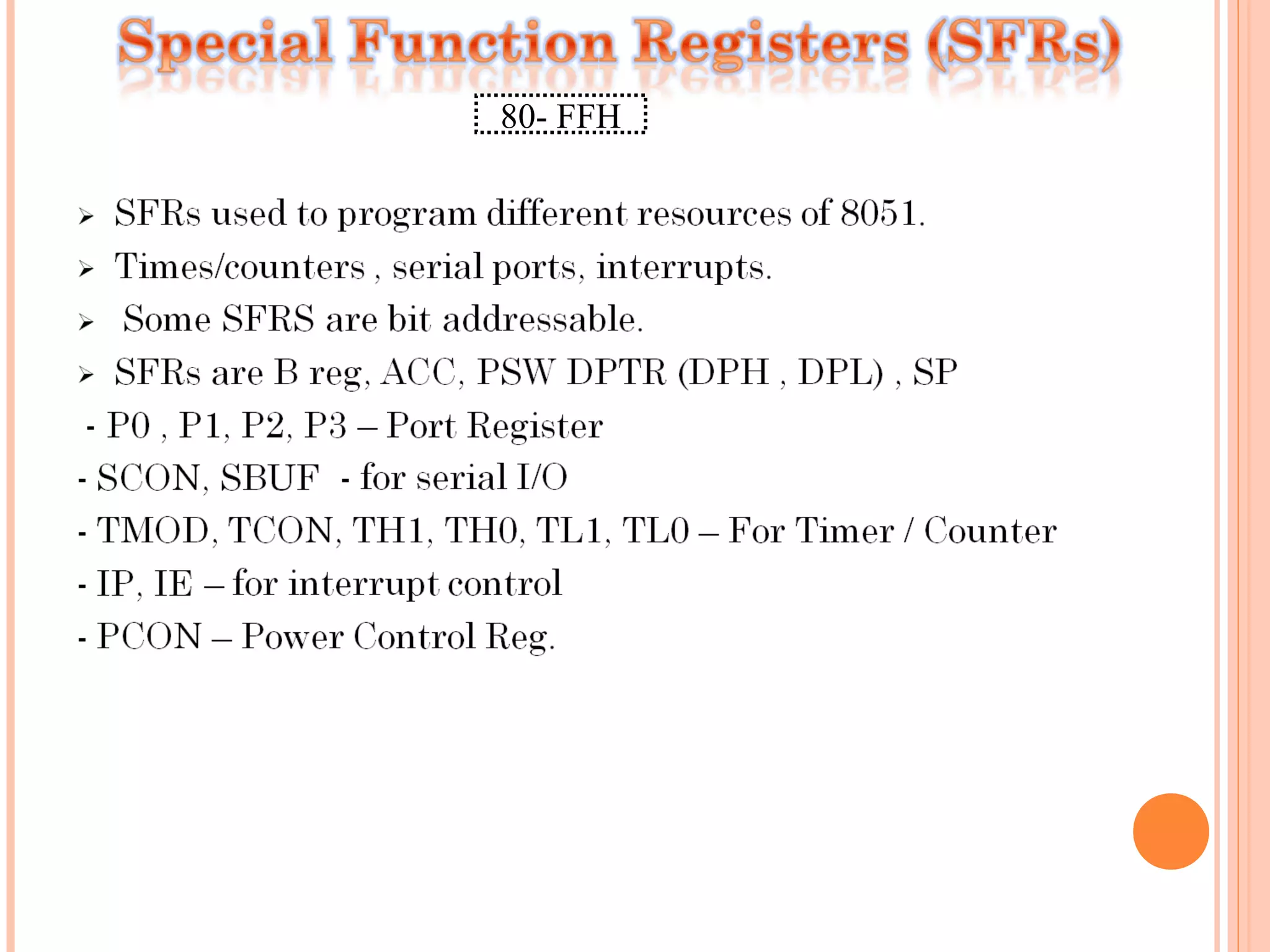
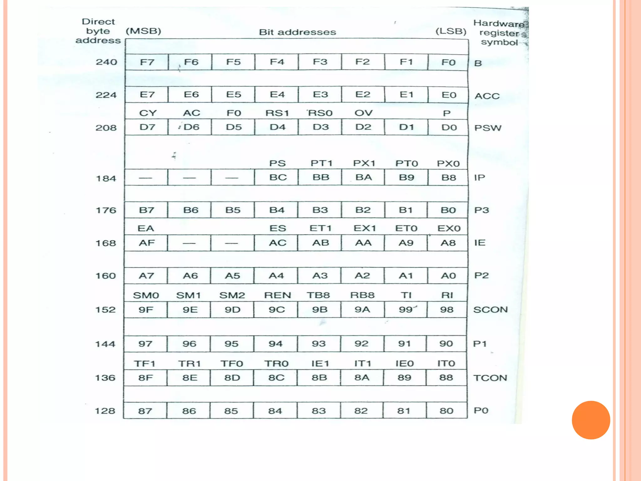
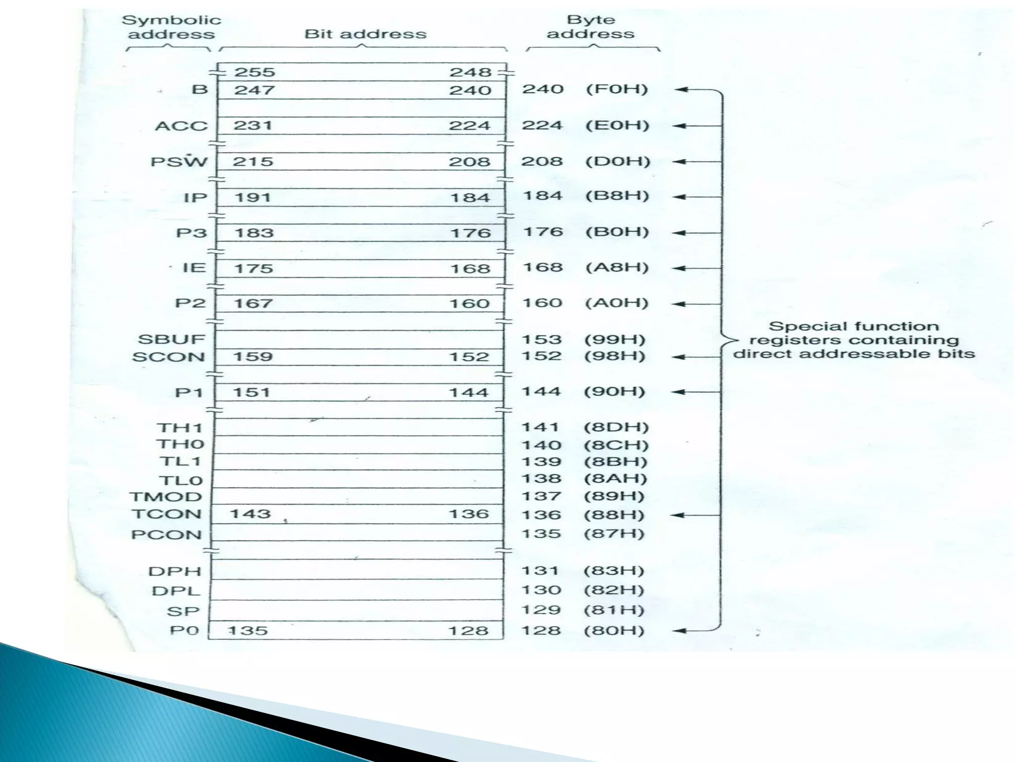
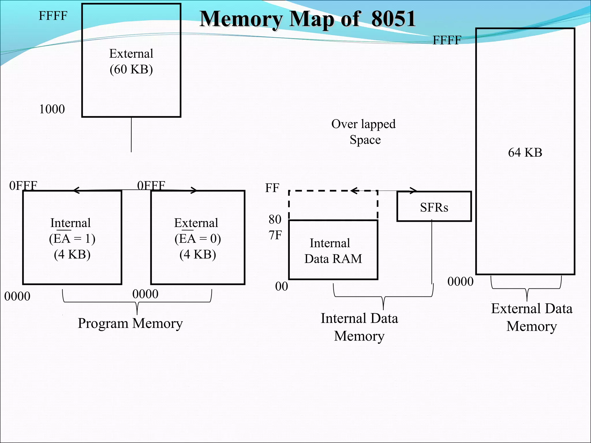
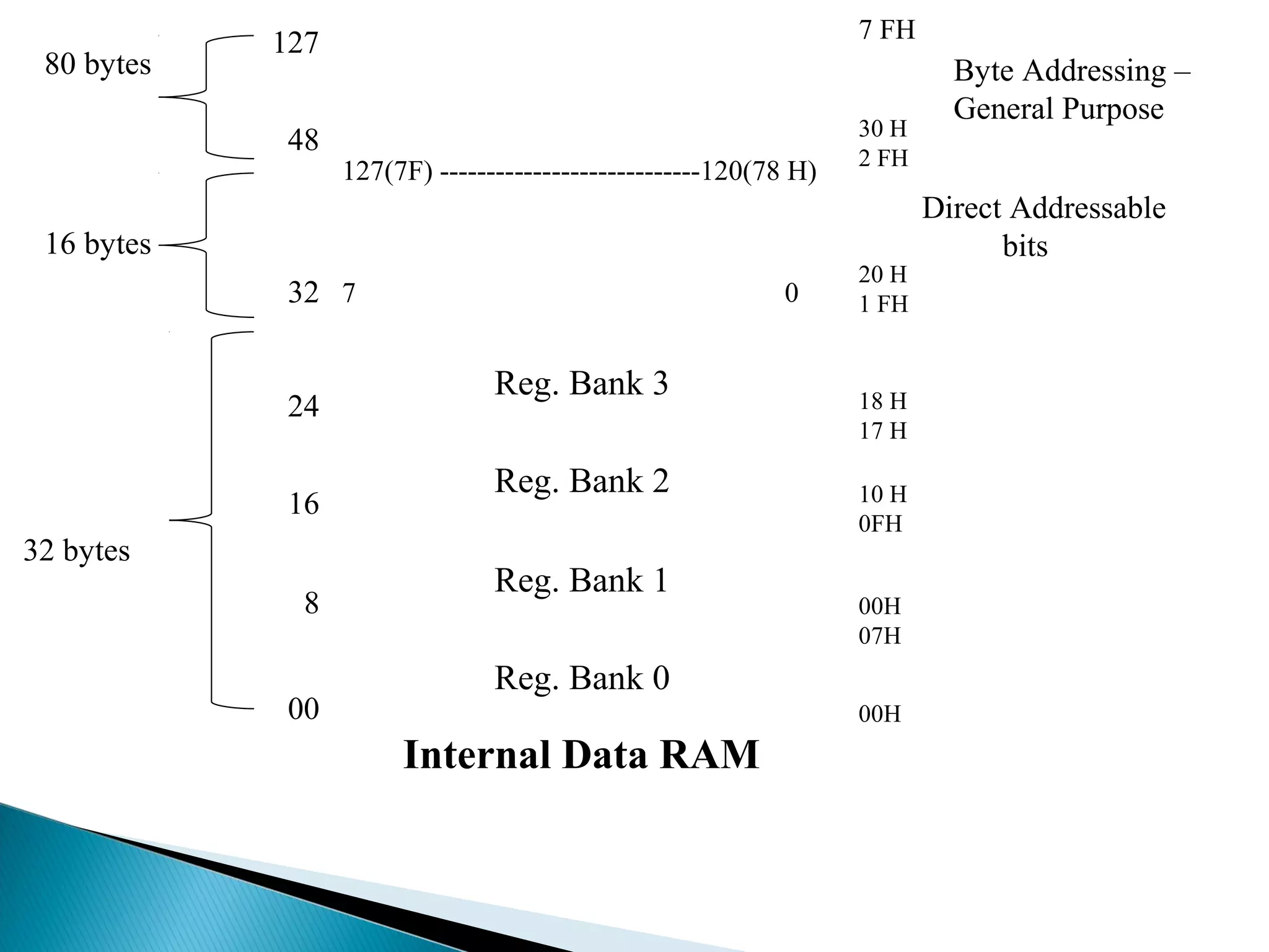
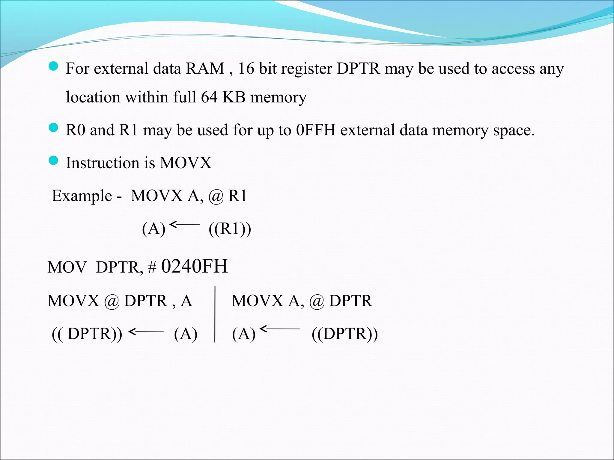
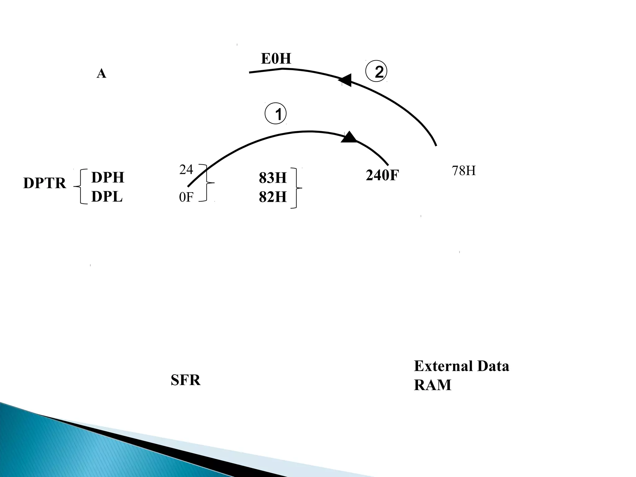
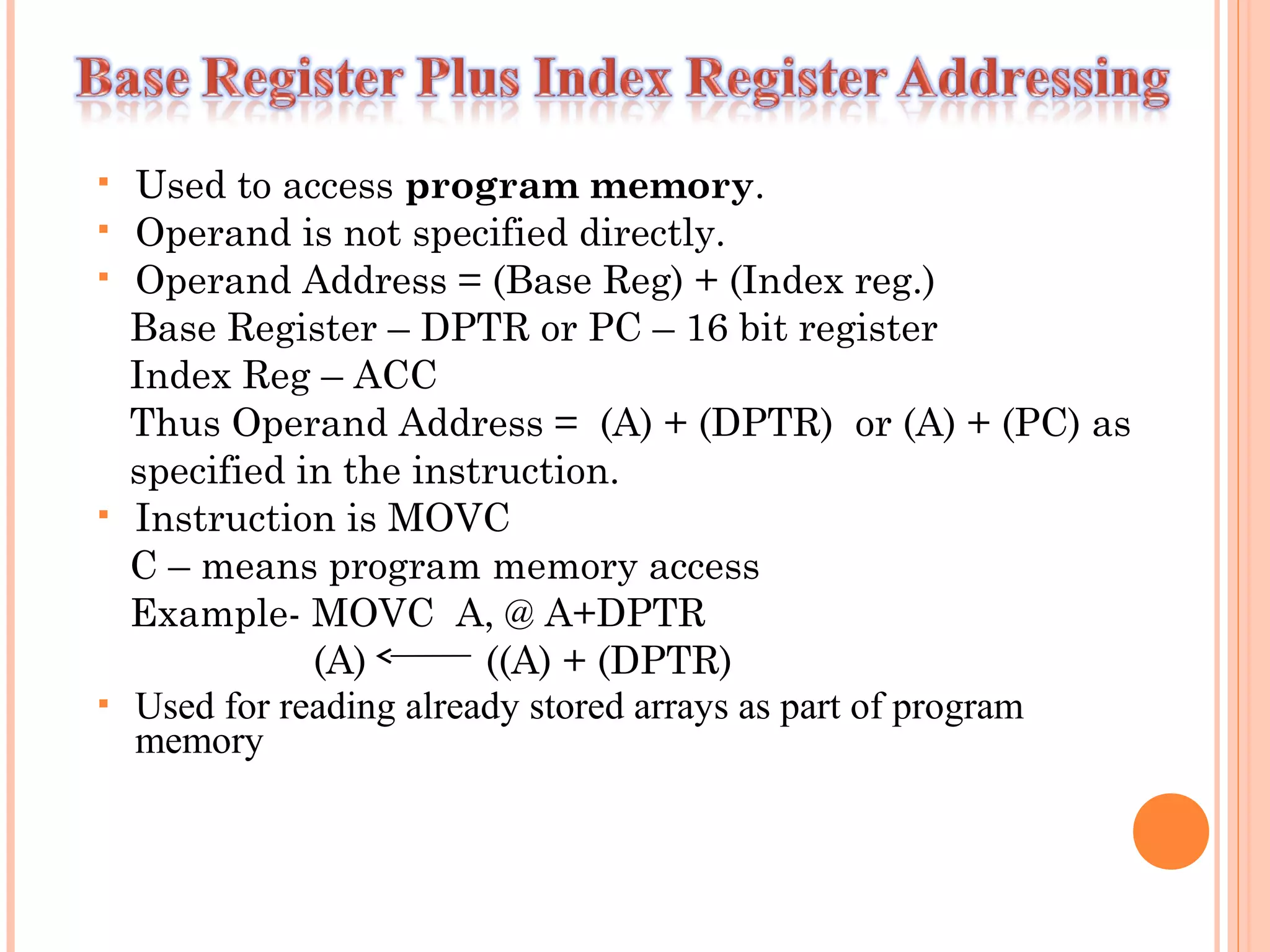
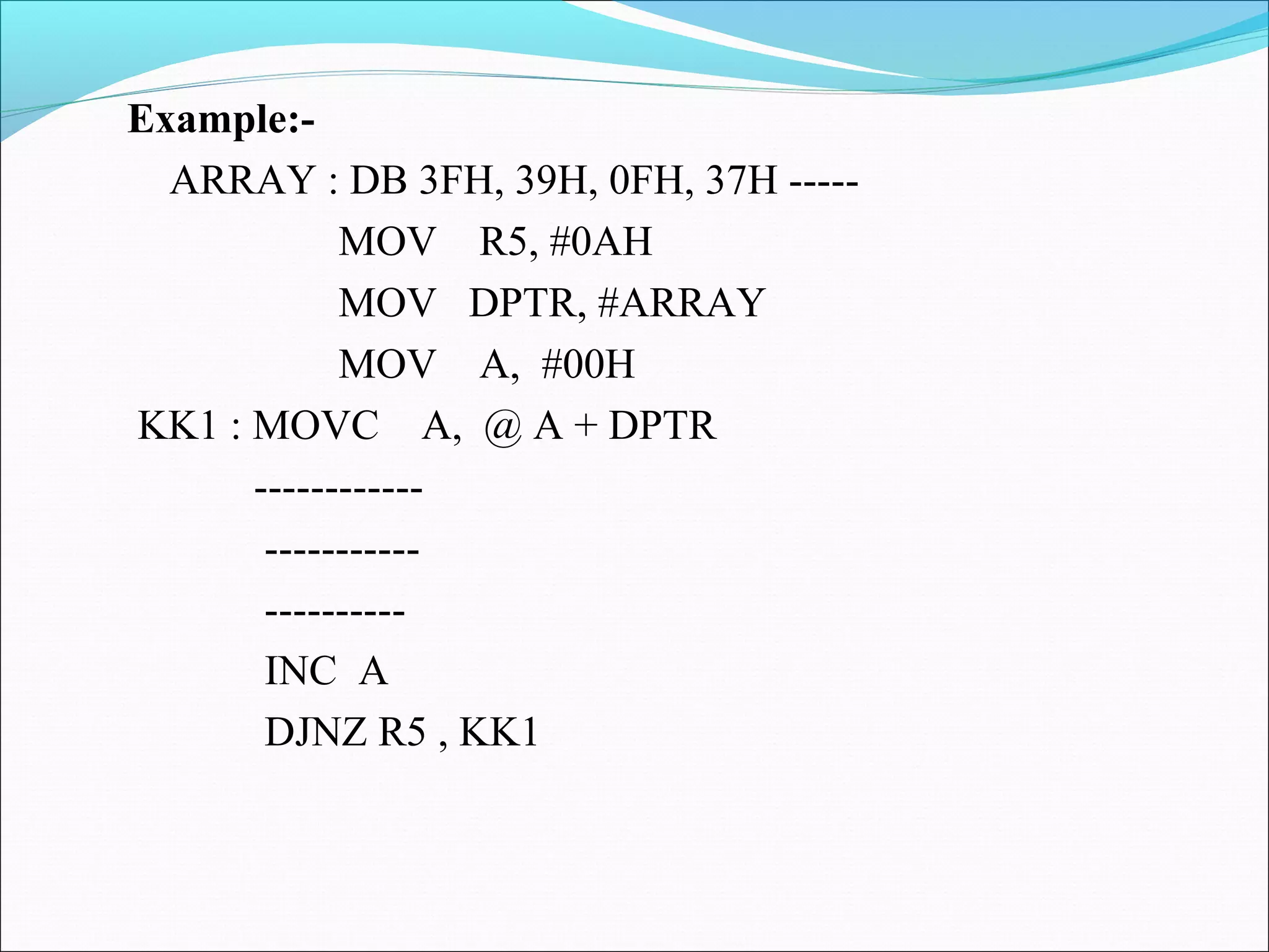
Usage of memory resources including program and data memory along with special function registers.
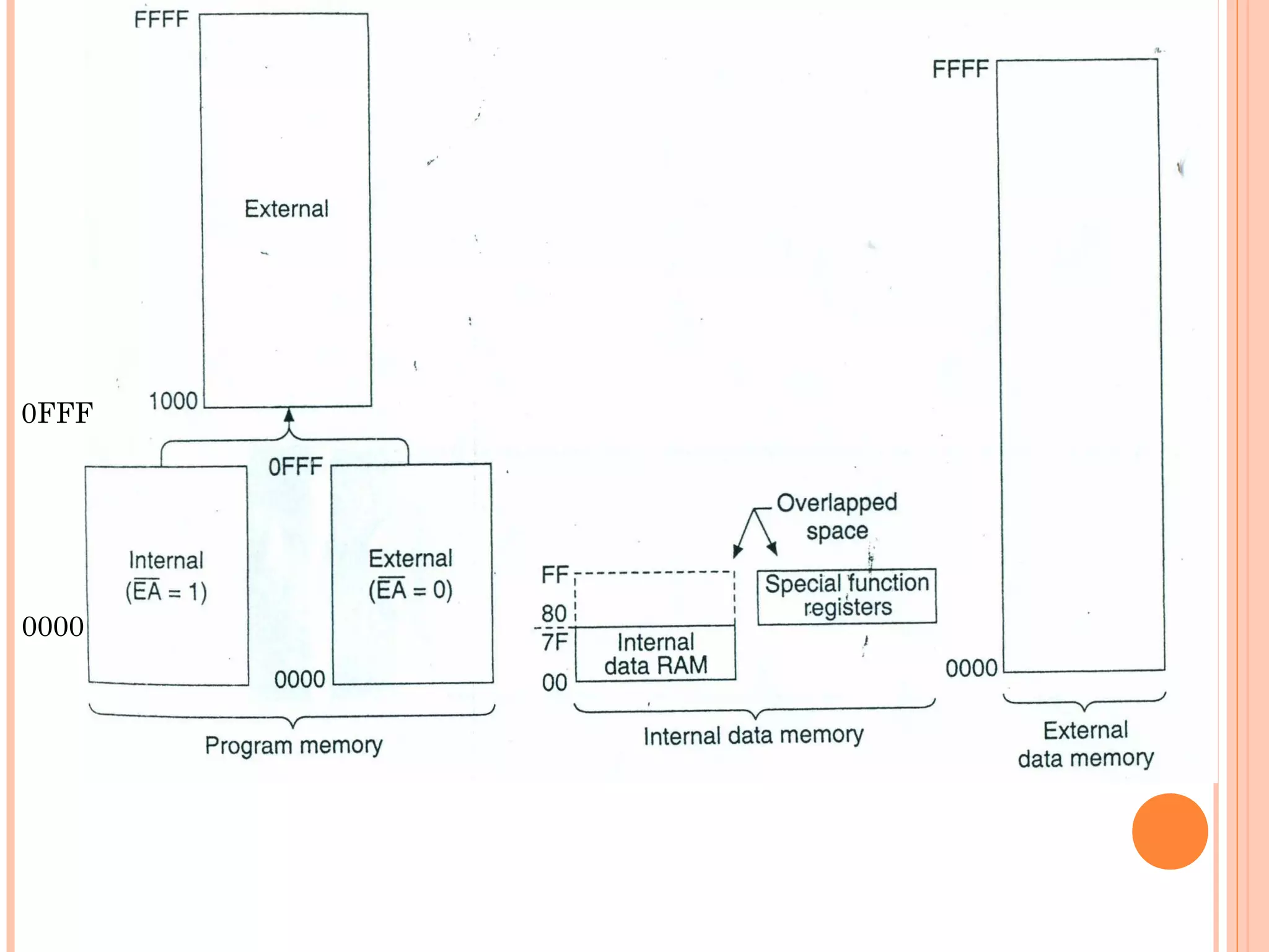
Structure of internal and external memory, detailing RAM and program memory layout.
Structure of internal and external memory, detailing RAM and program memory layout.
Structure of internal and external memory, detailing RAM and program memory layout.
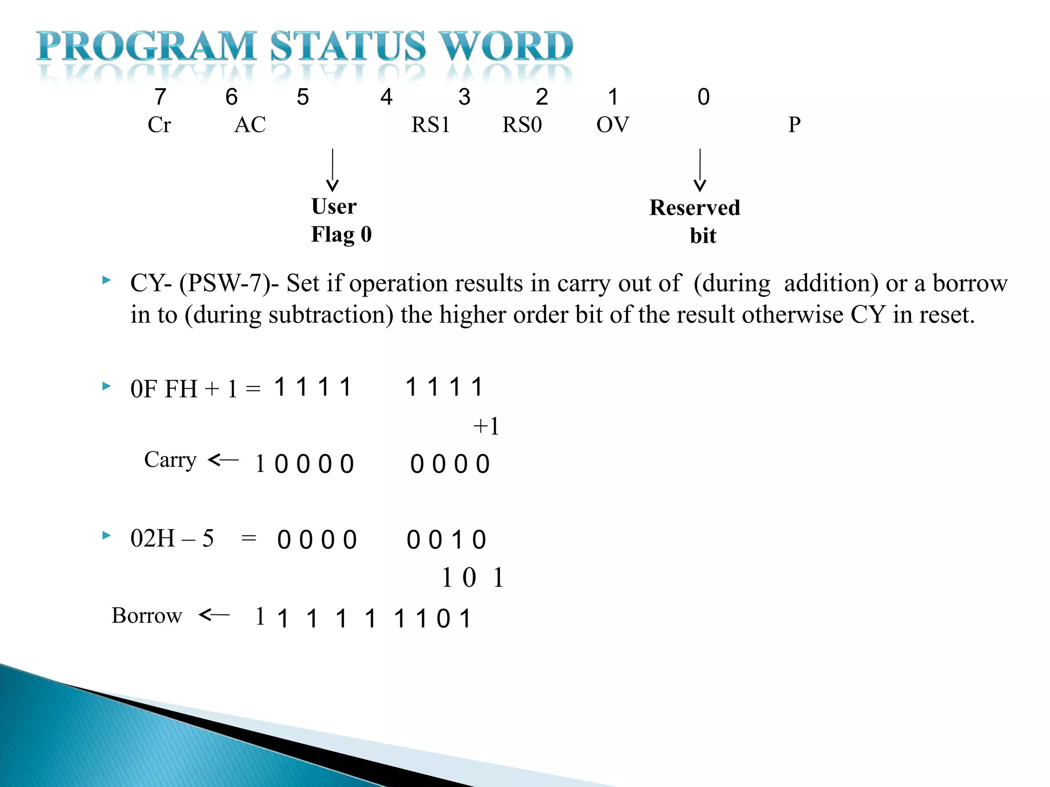
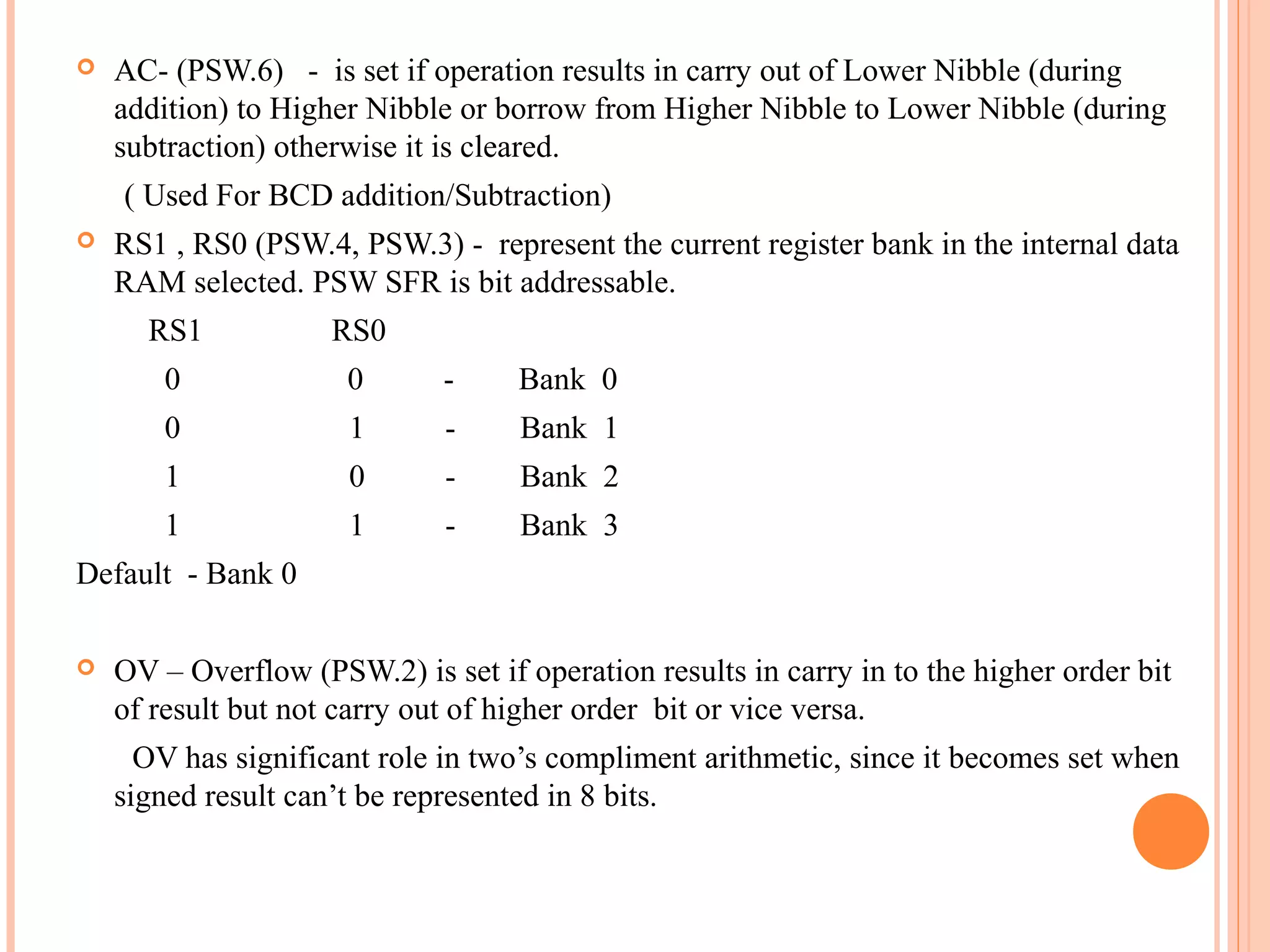
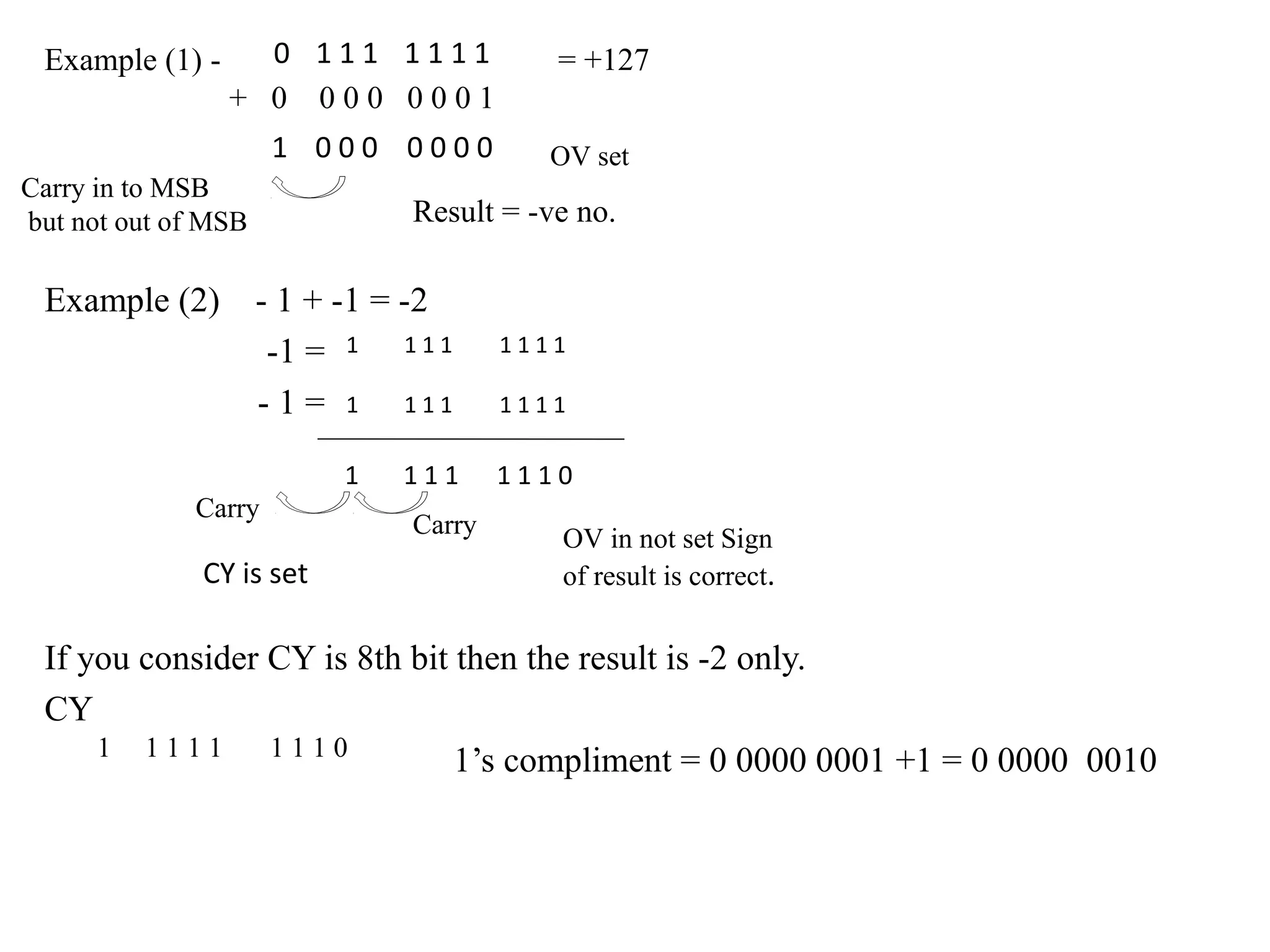
Explanation of PSW bits and their functionalities including carry and overflow flags.
Explanation of PSW bits and their functionalities including carry and overflow flags.
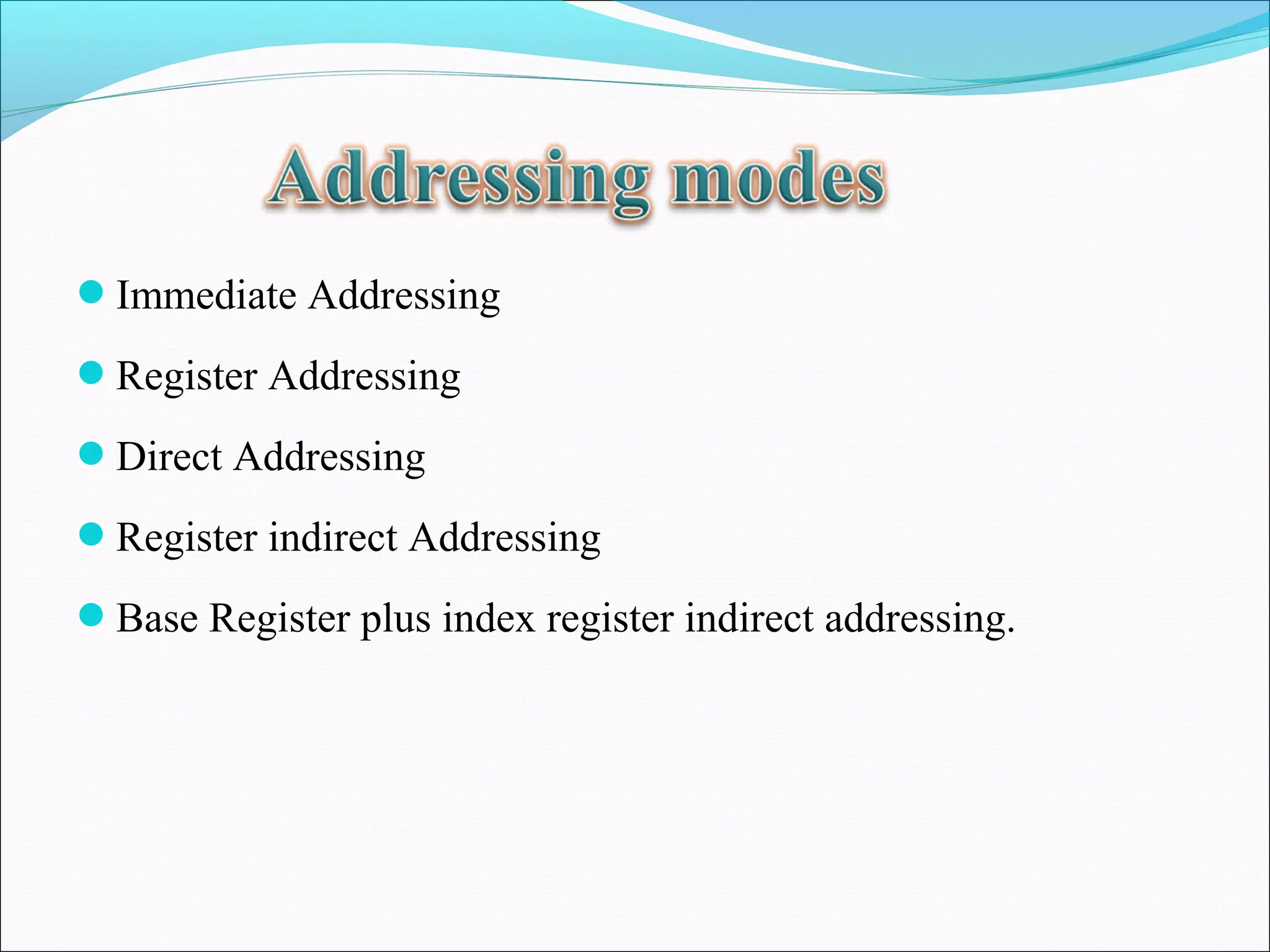
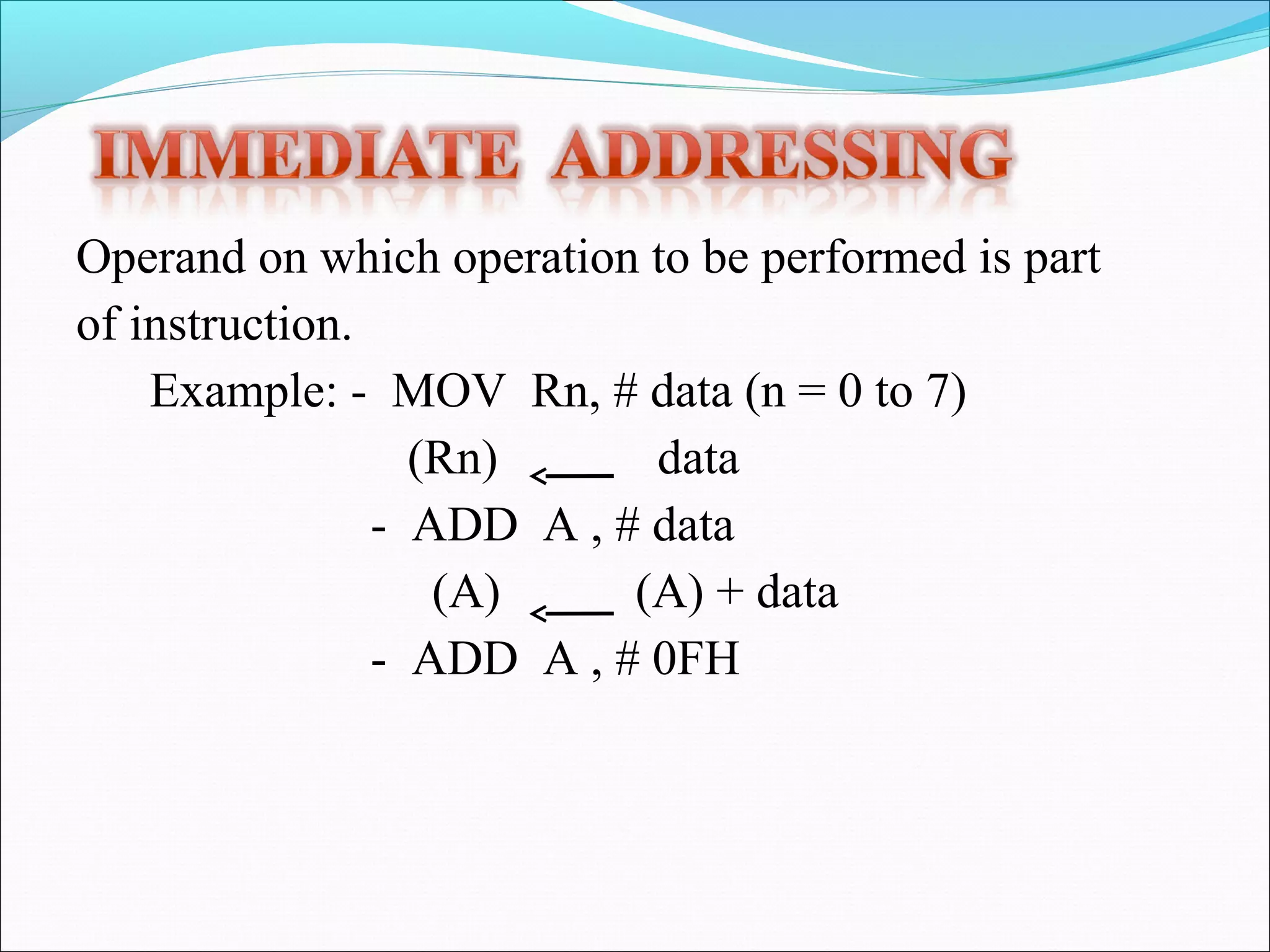
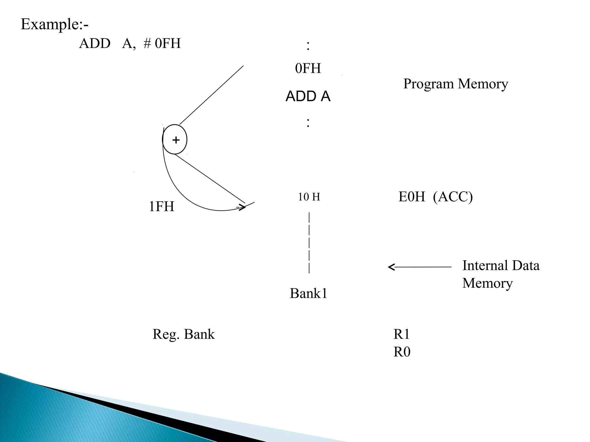
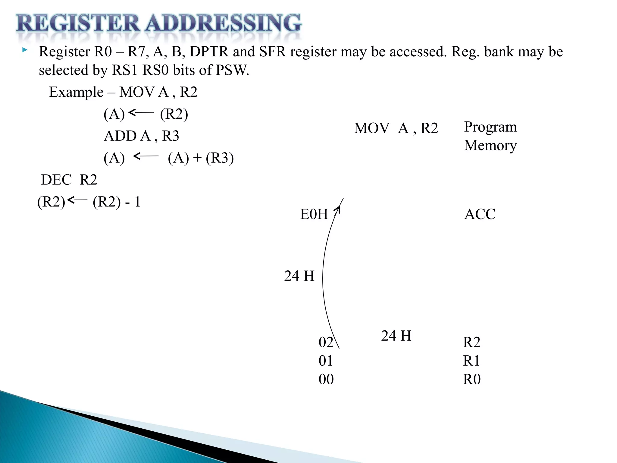
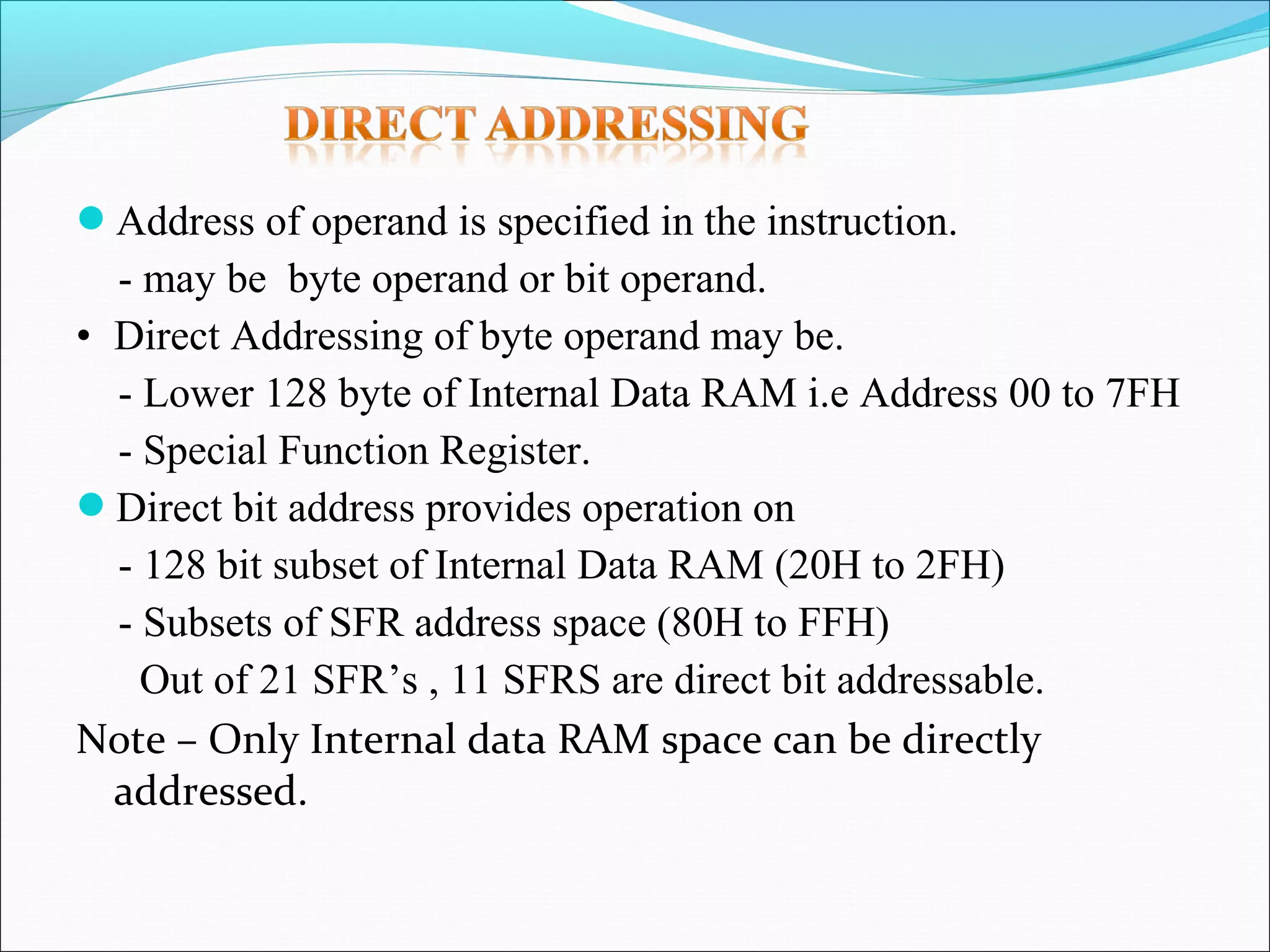
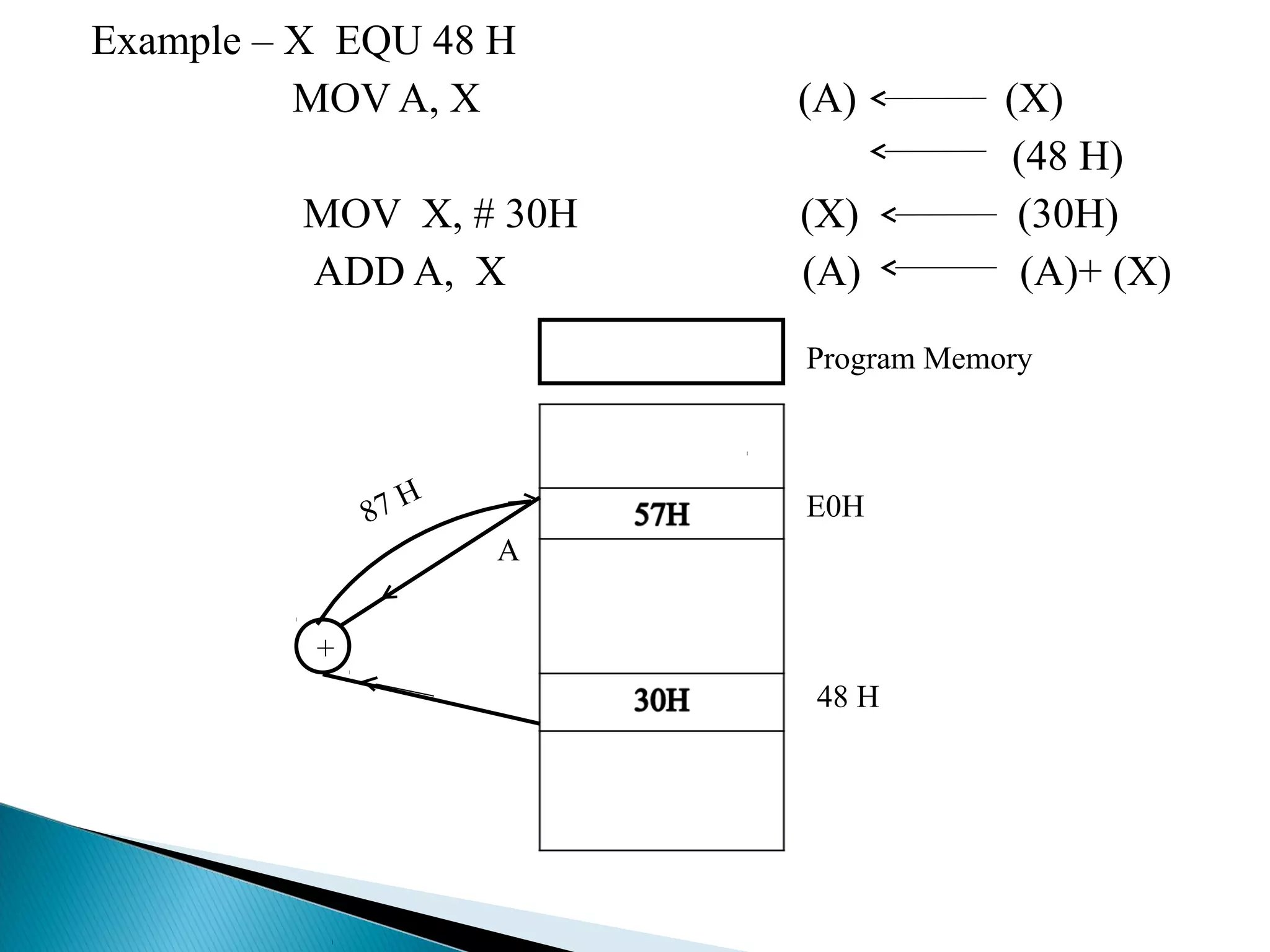
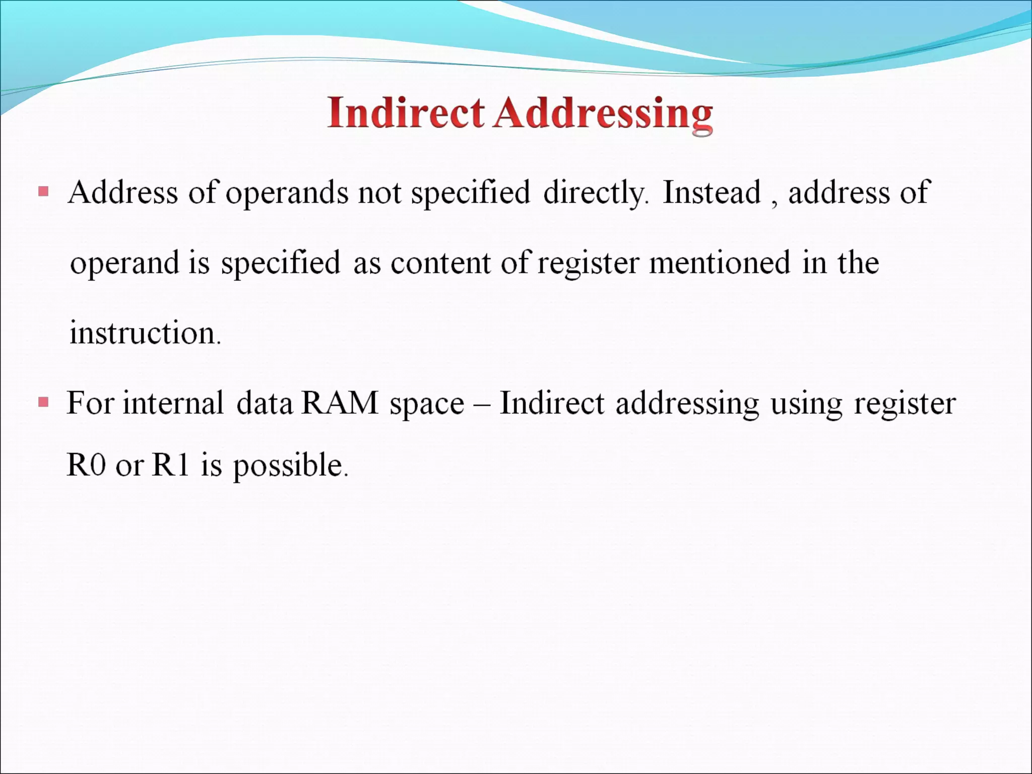
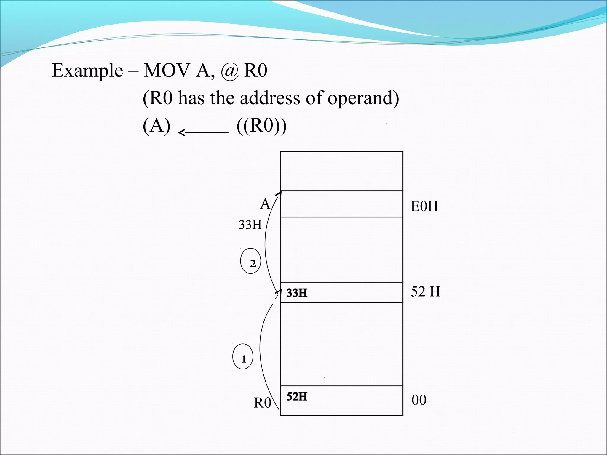
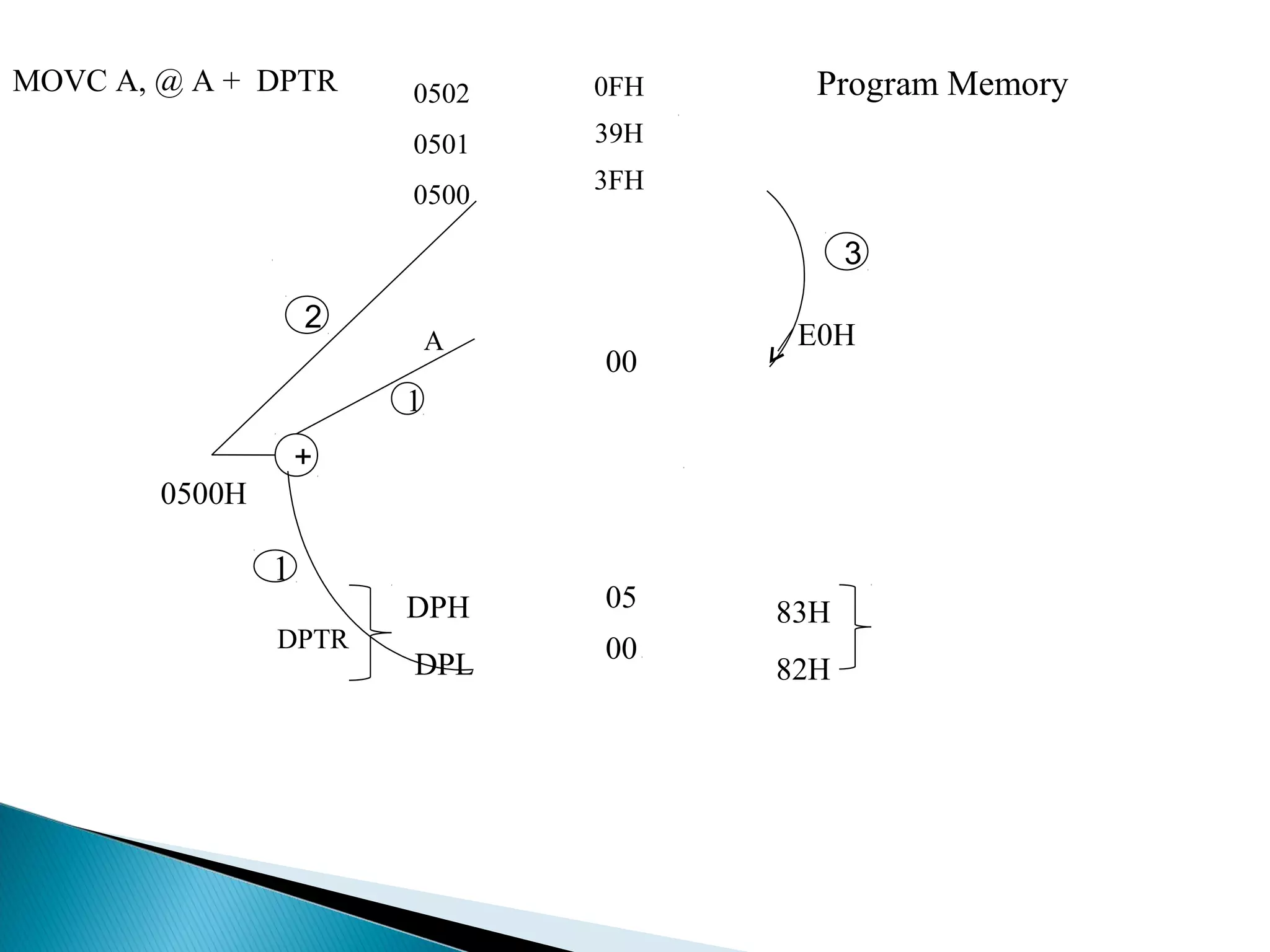
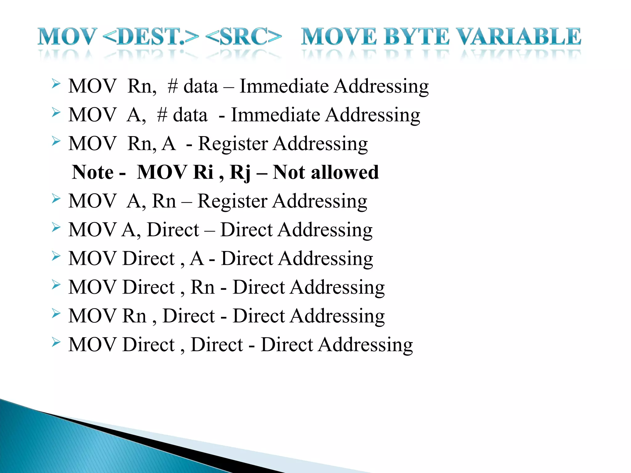
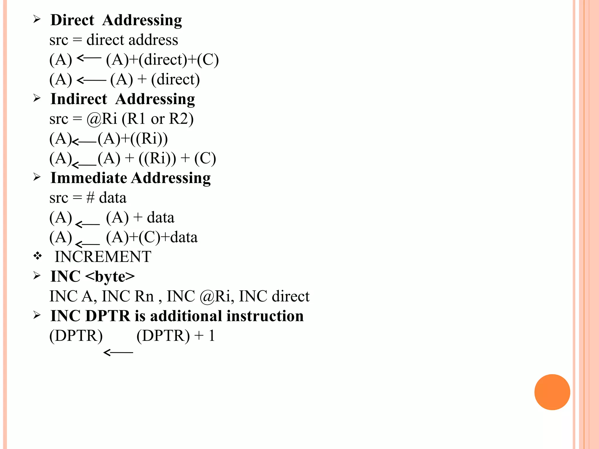
Various addressing modes: immediate, register, direct, and indirect along with examples.
Various addressing modes: immediate, register, direct, and indirect along with examples.
Various addressing modes: immediate, register, direct, and indirect along with examples.
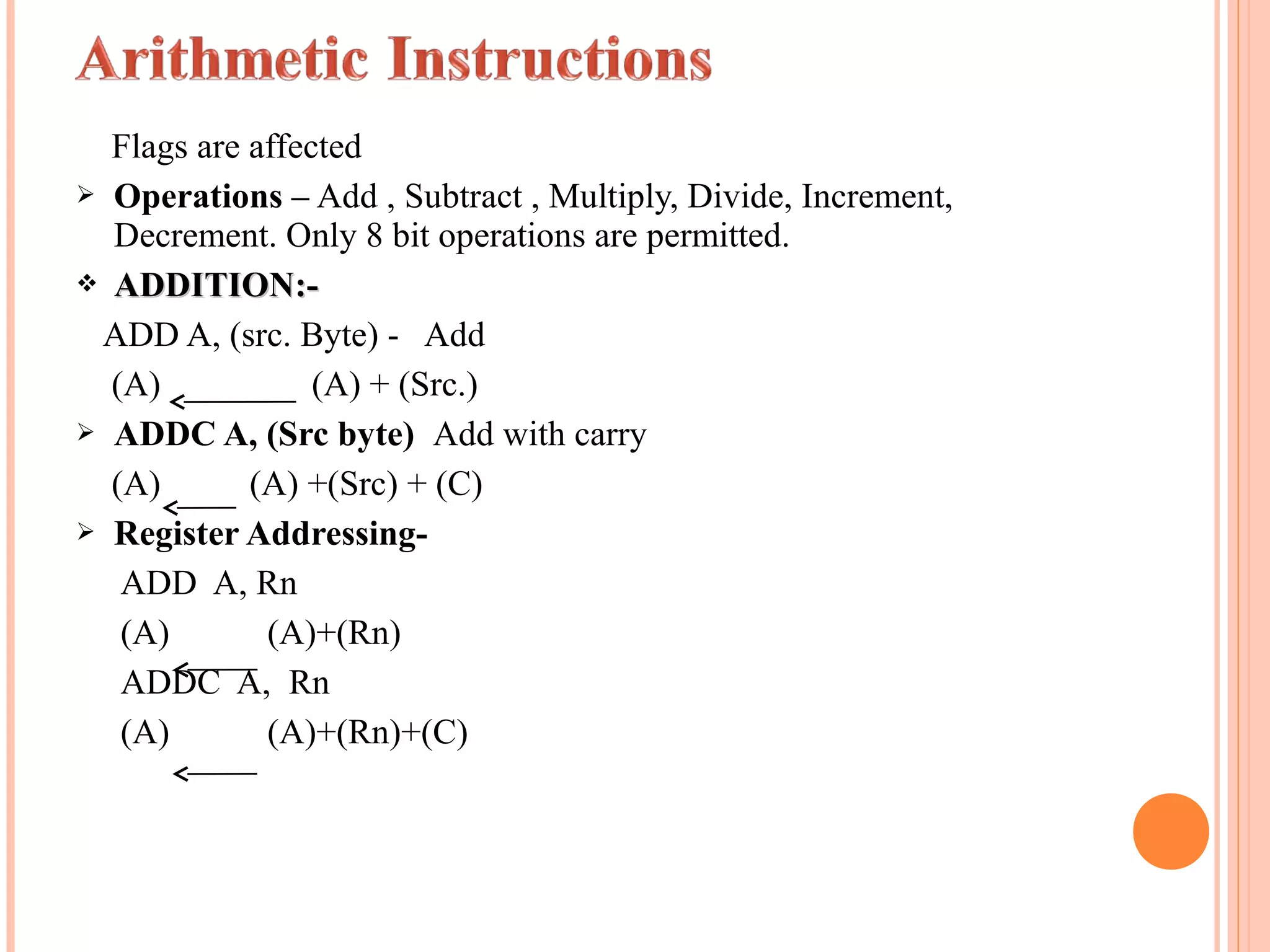
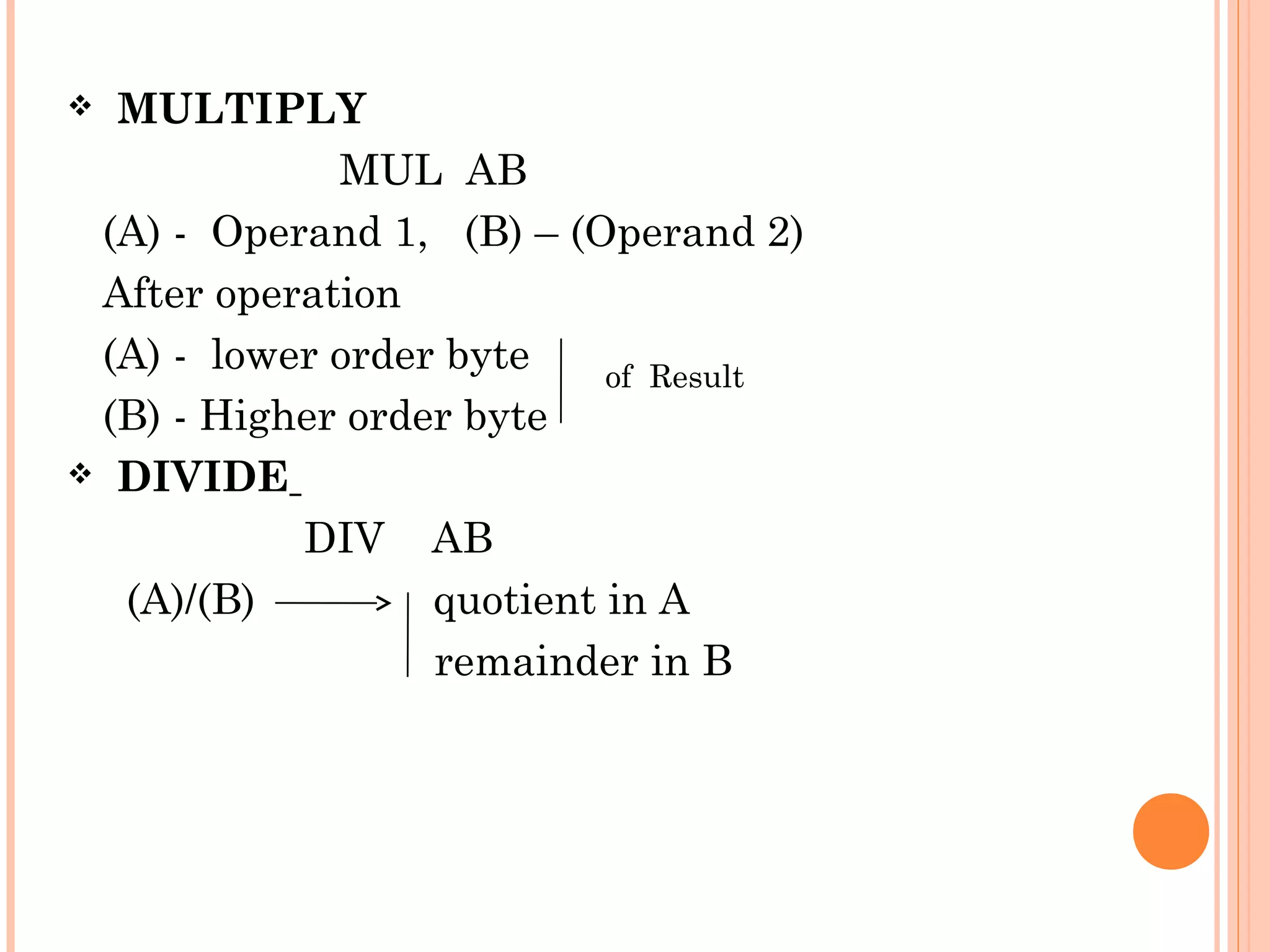
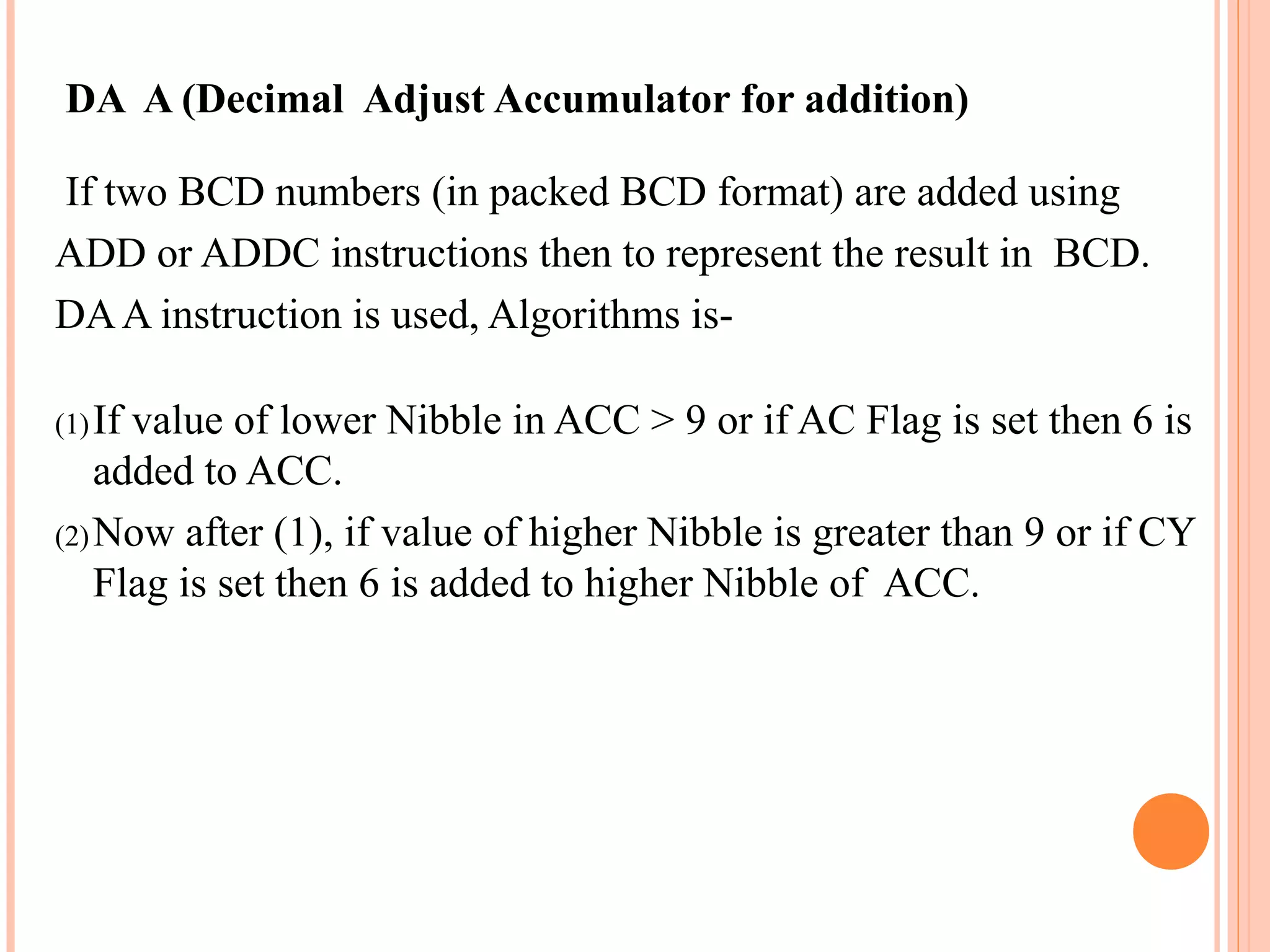
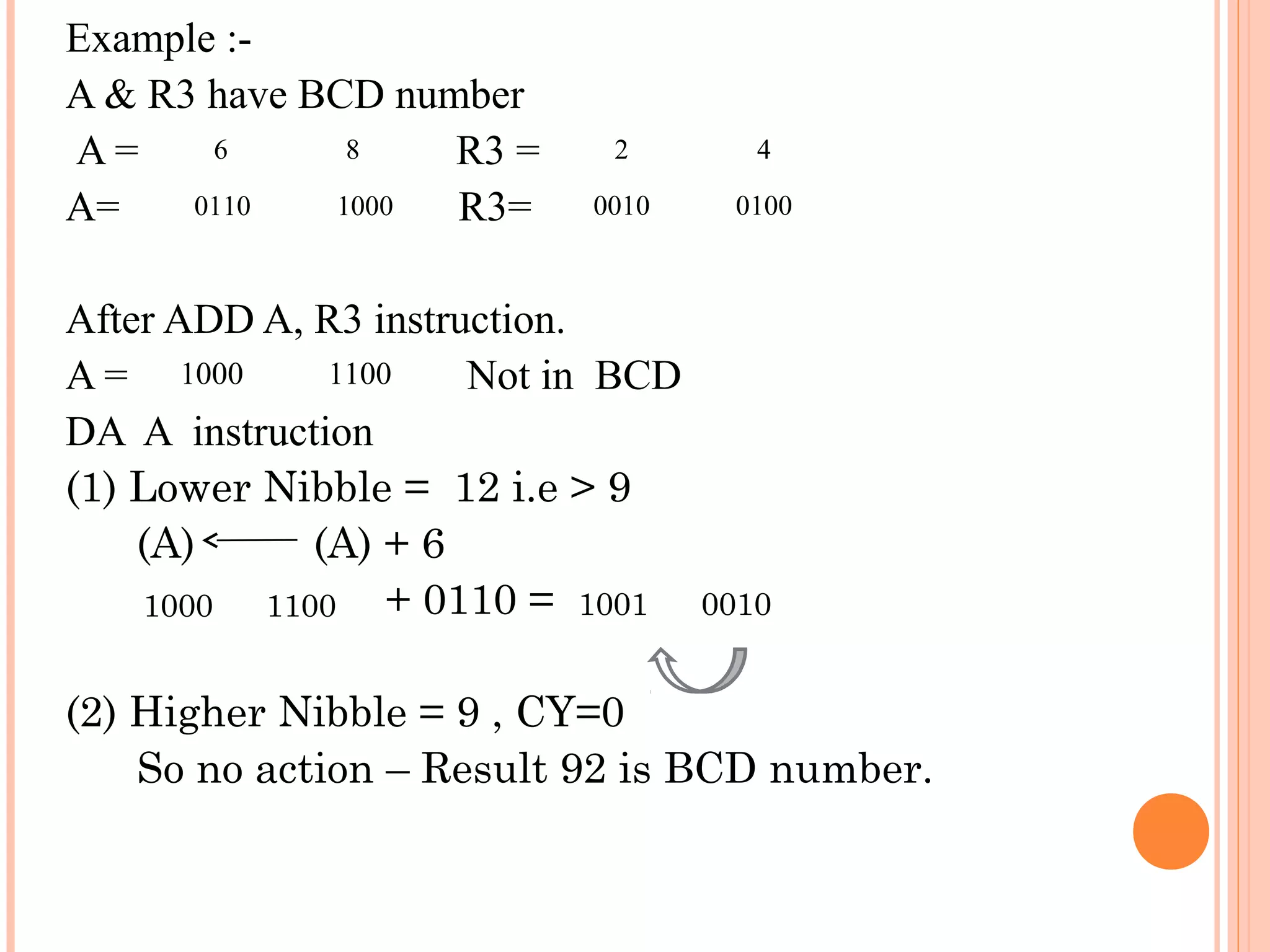
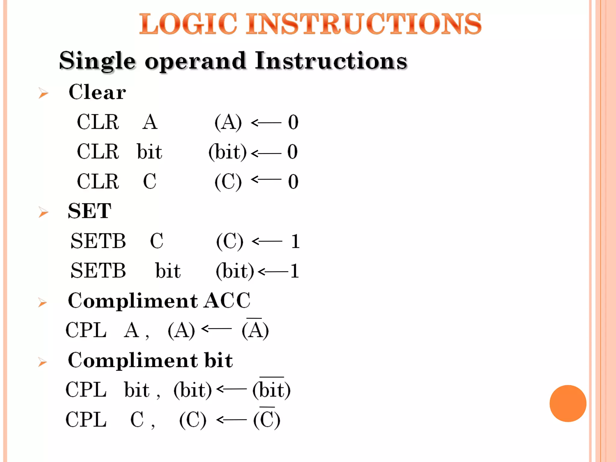
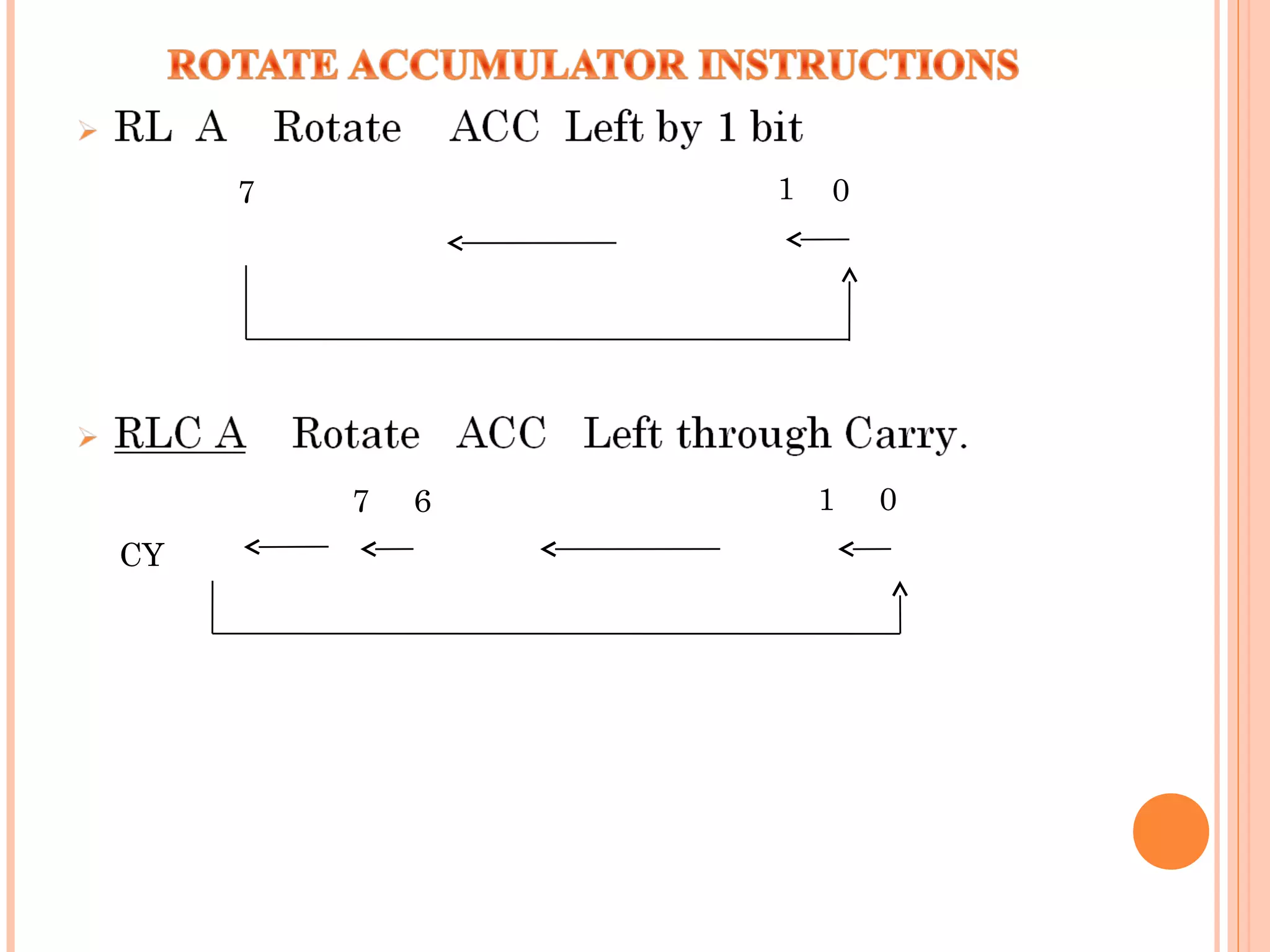
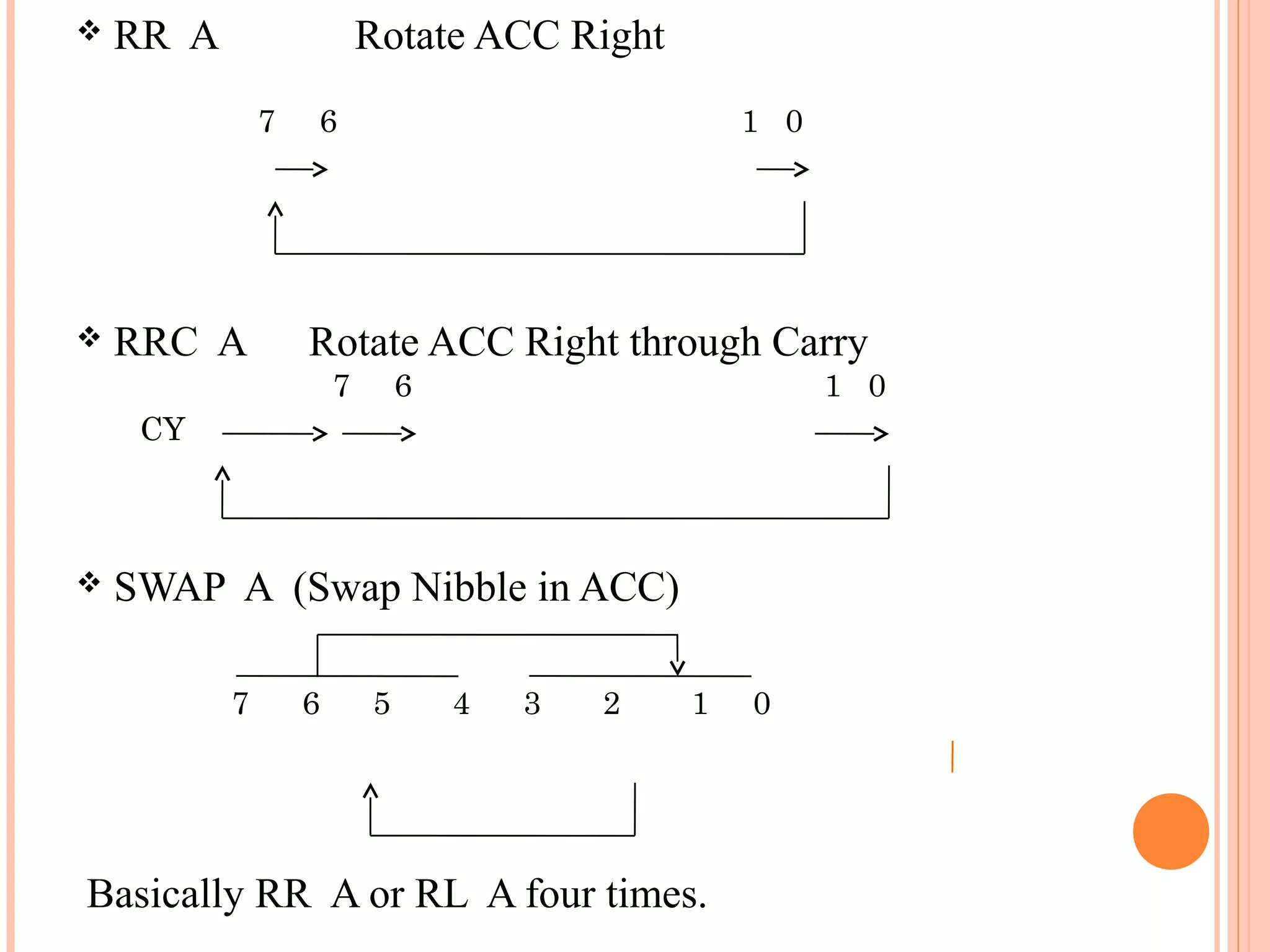
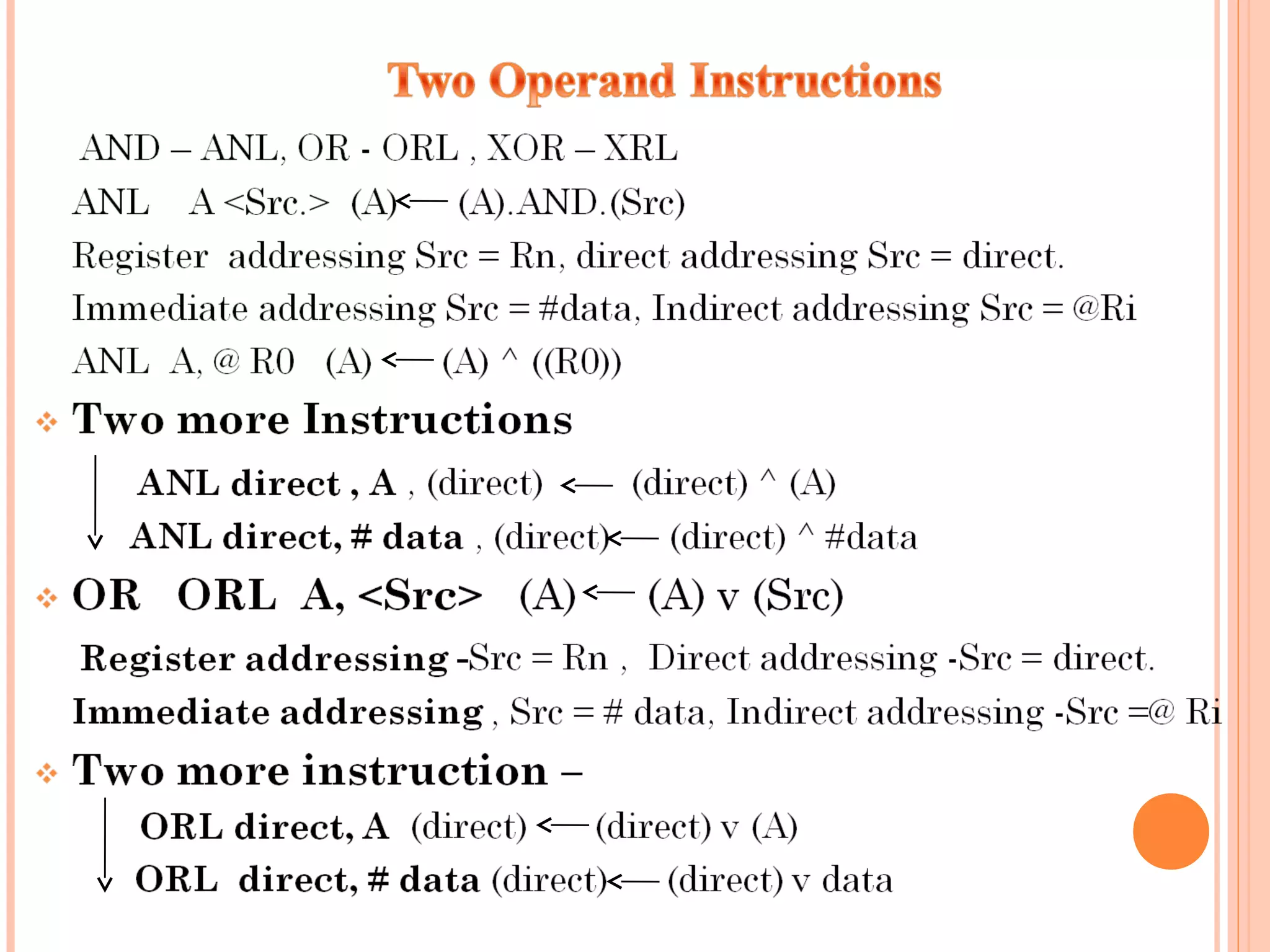
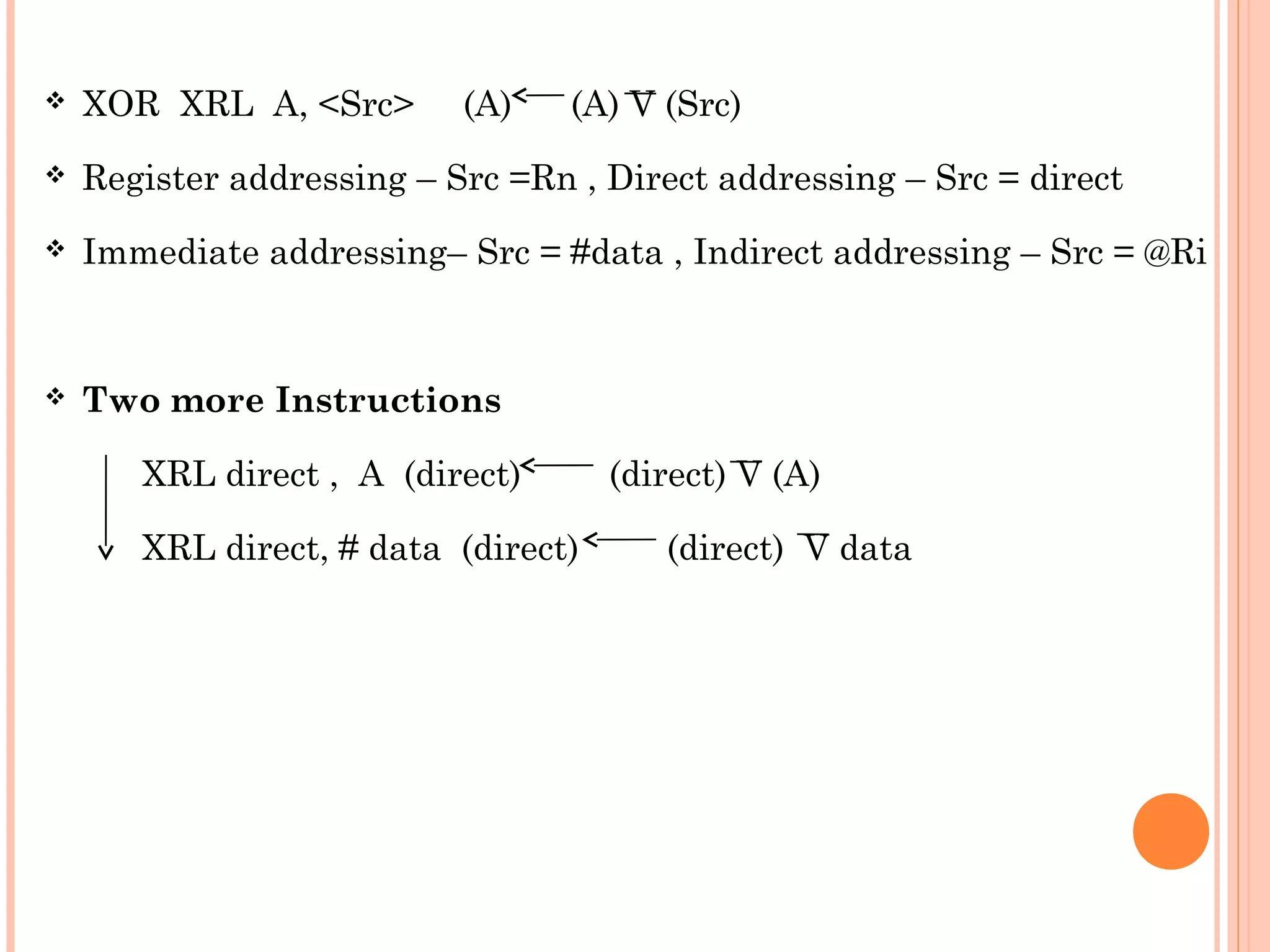
Instructions for data transfer, arithmetic operations, and handling BCD for additions/subtractions.
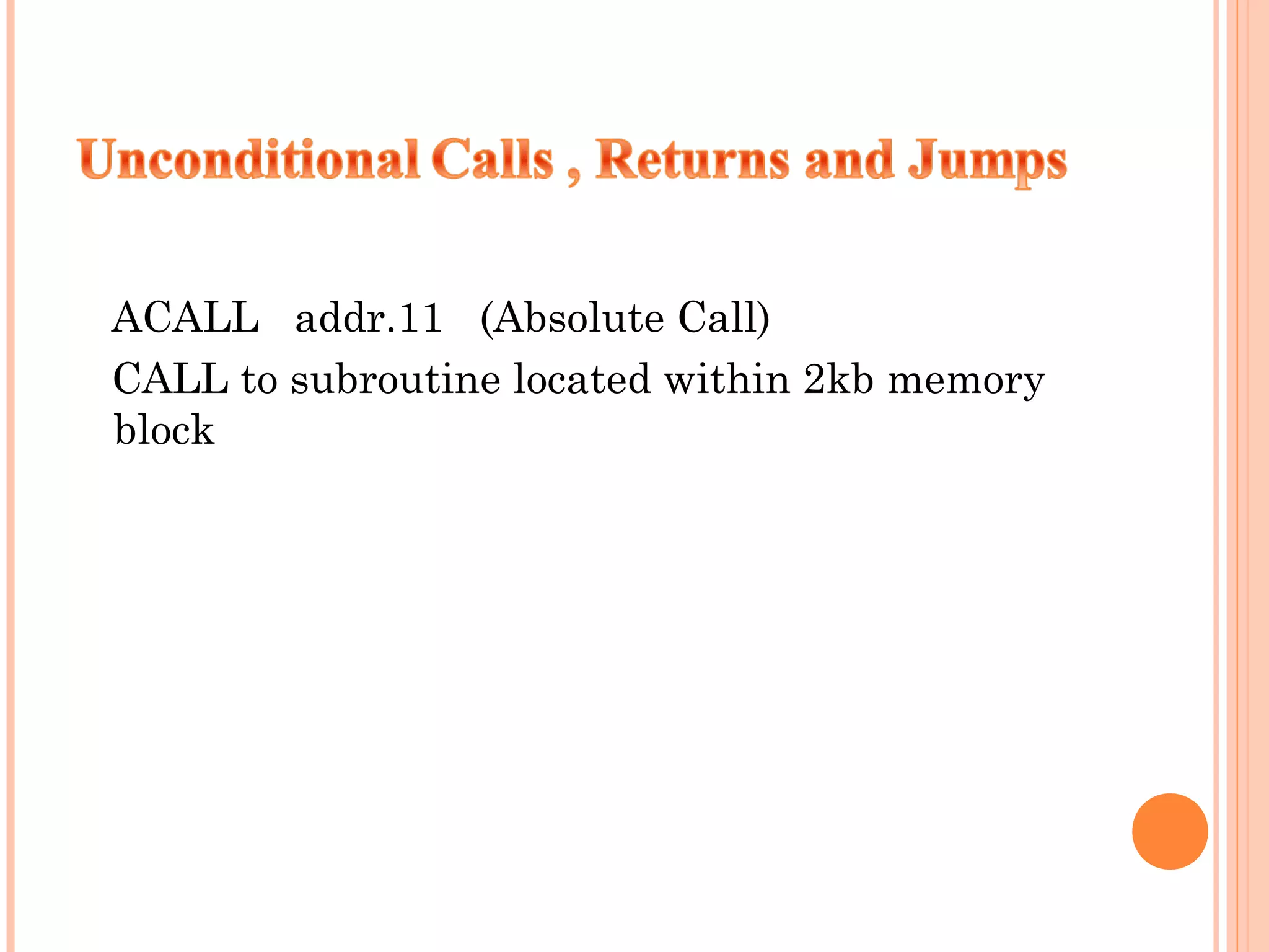
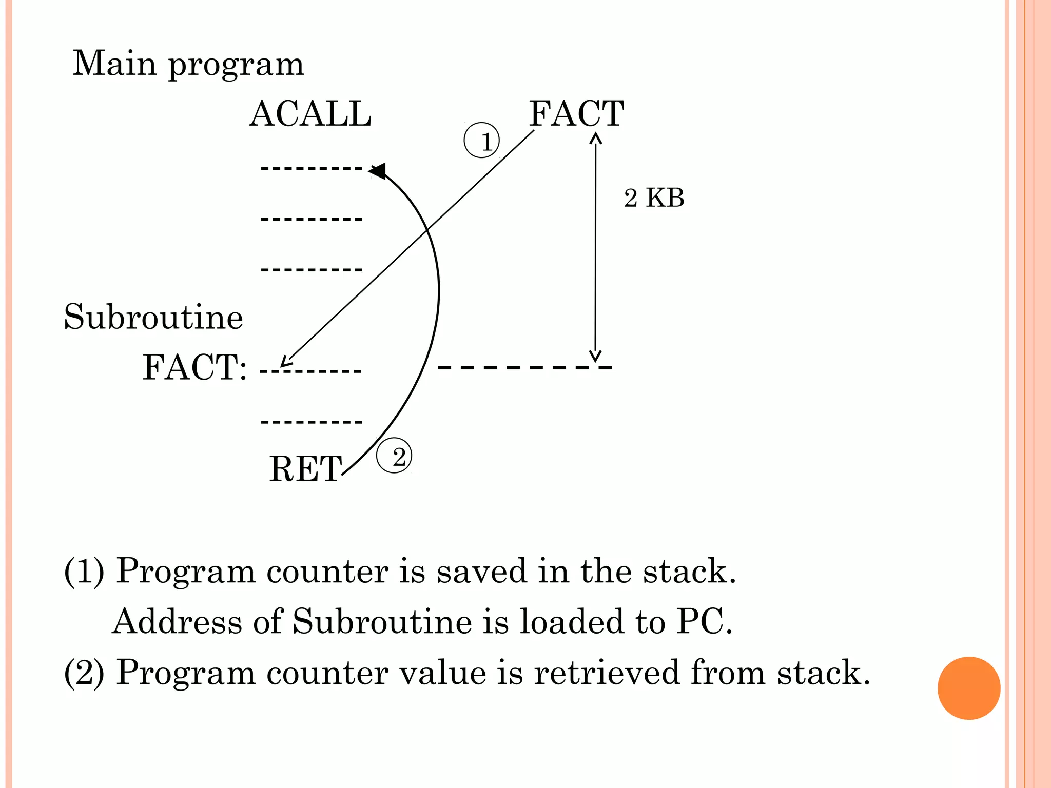
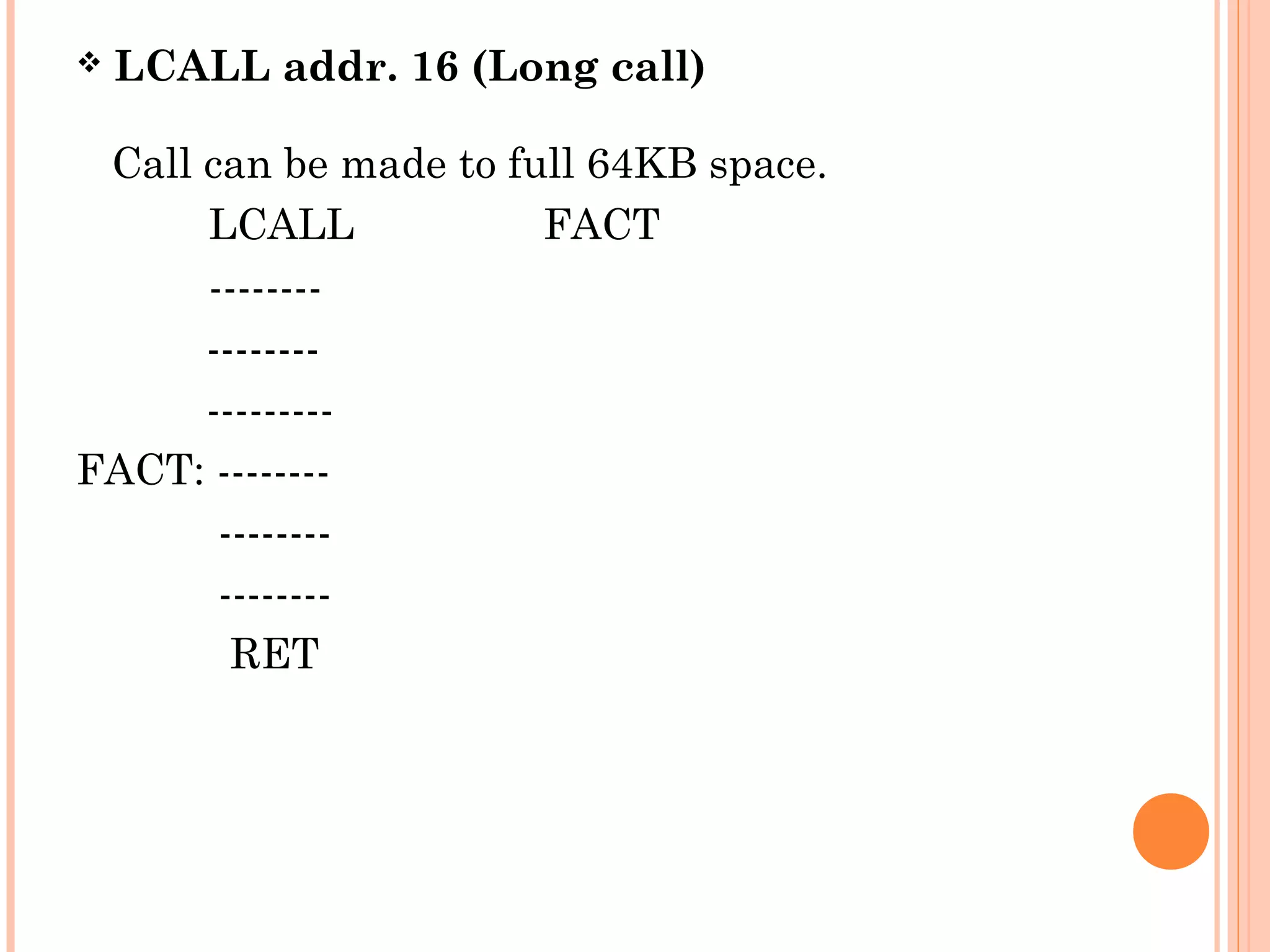
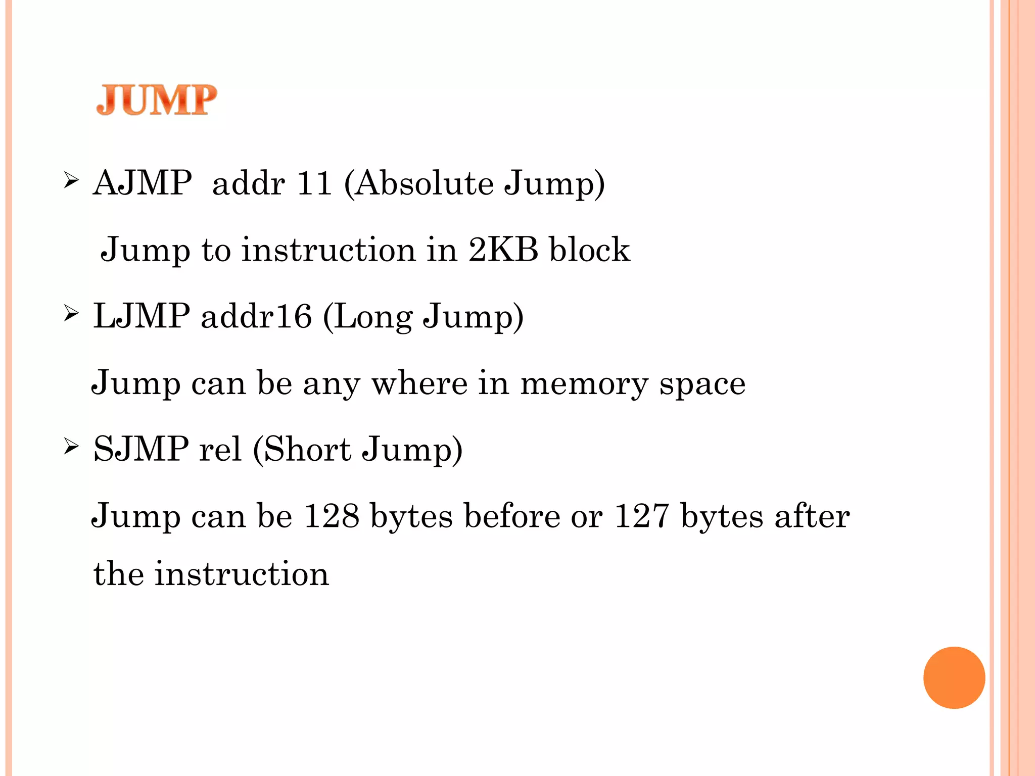
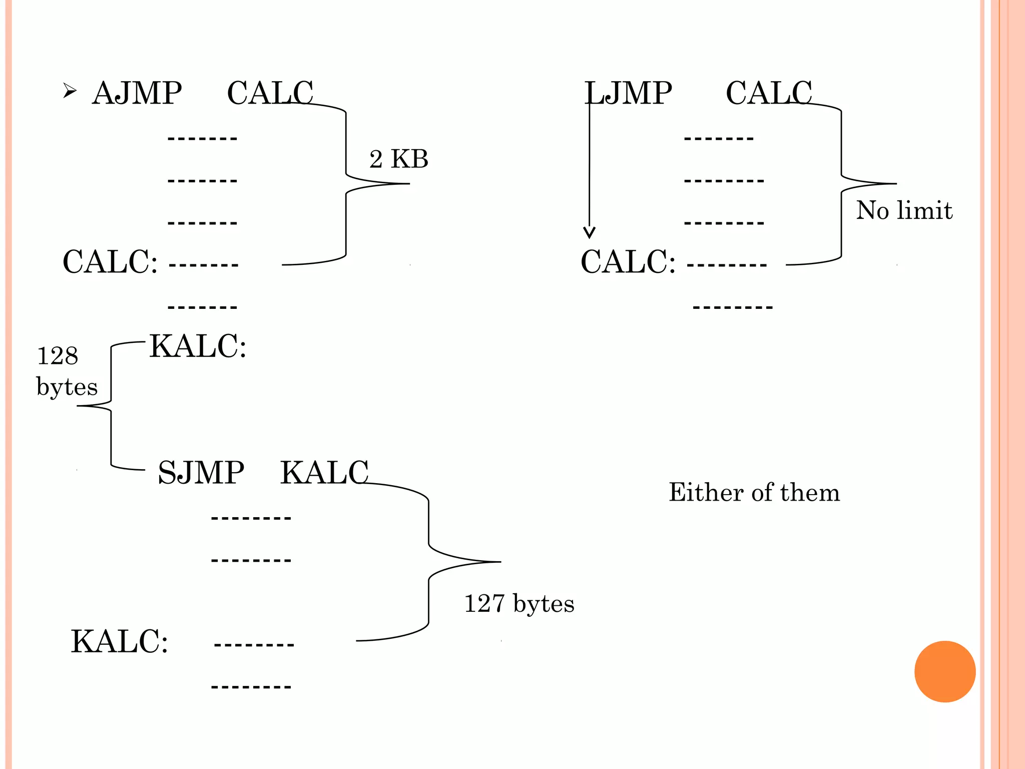
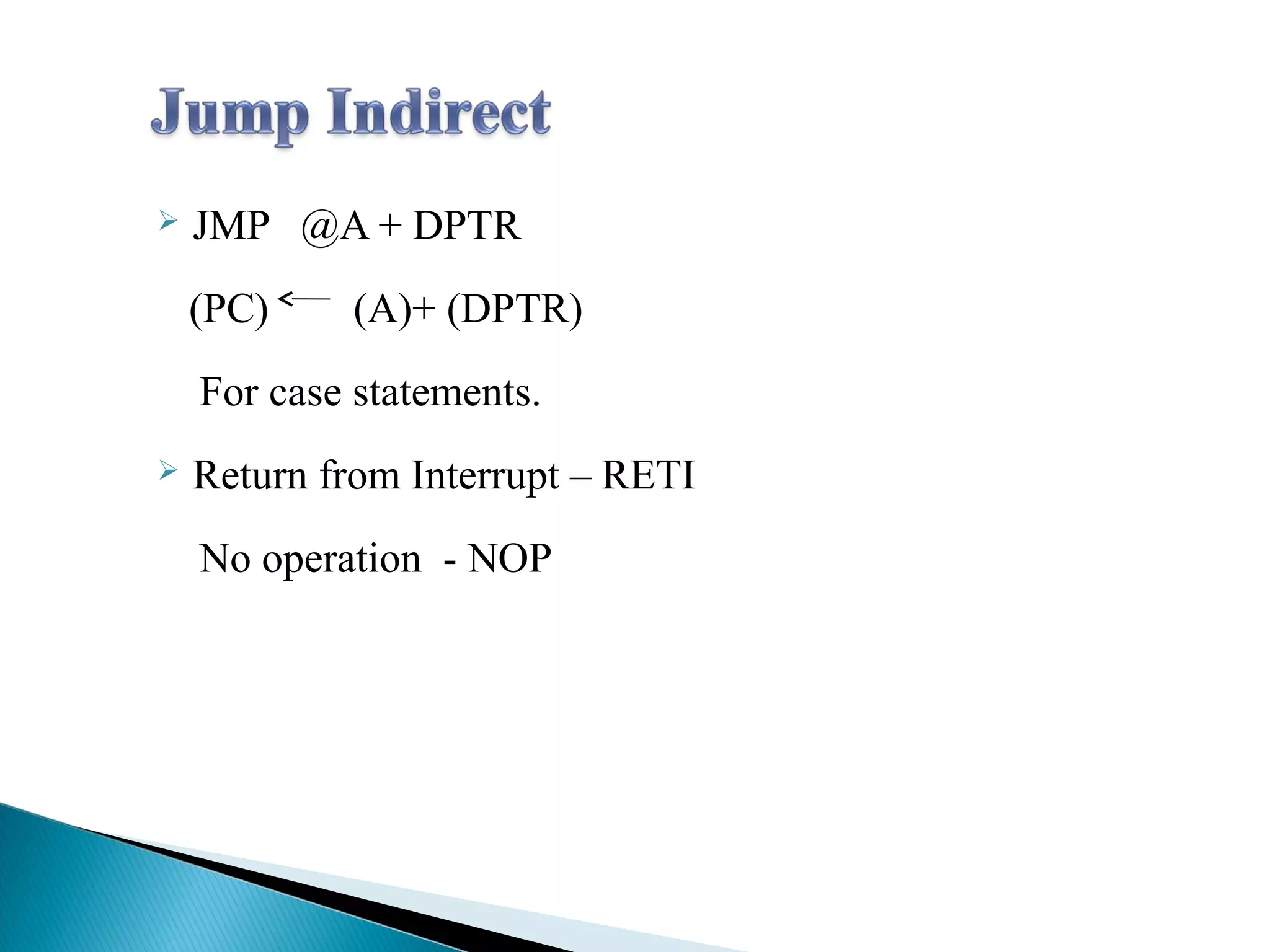
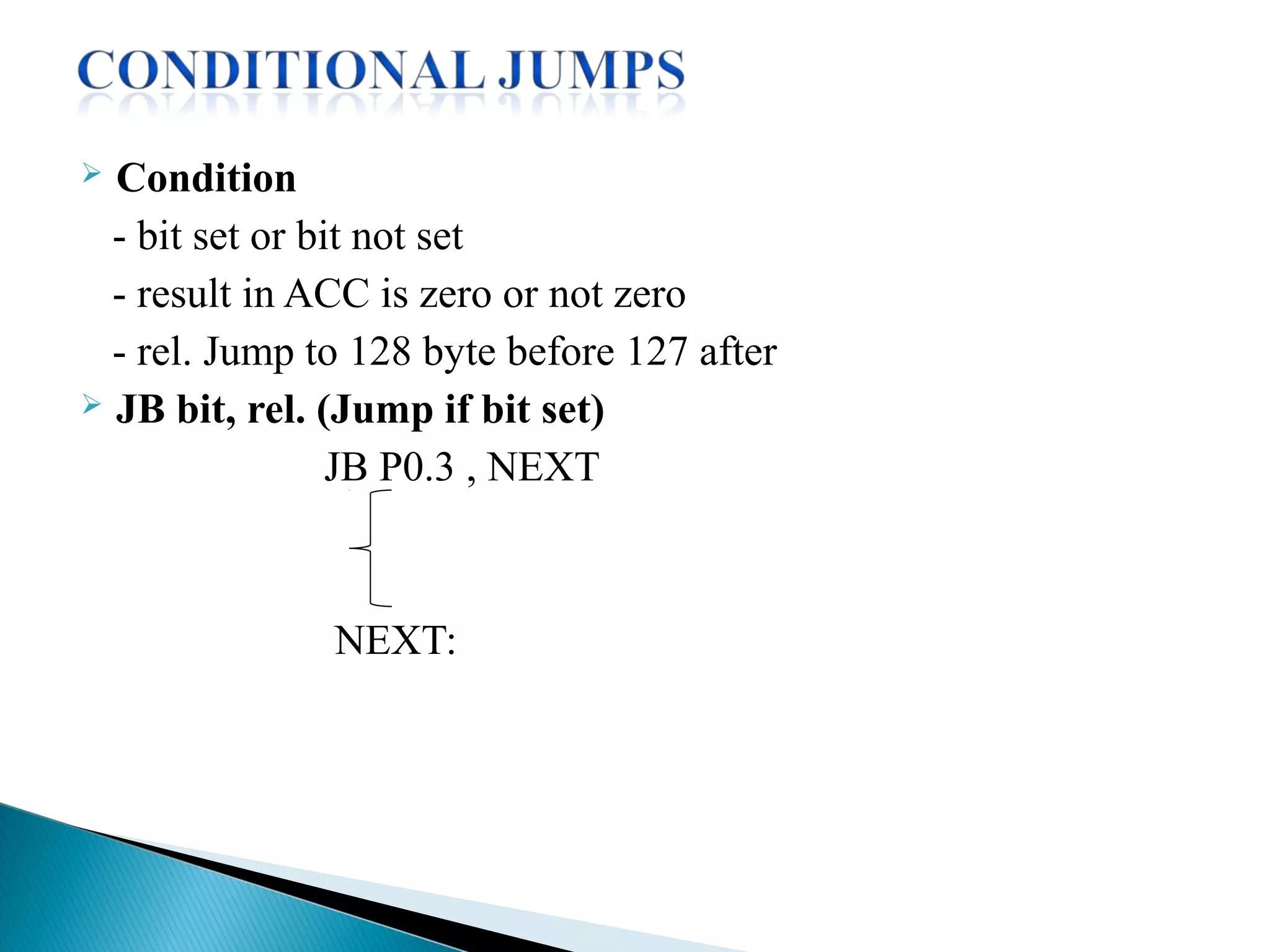
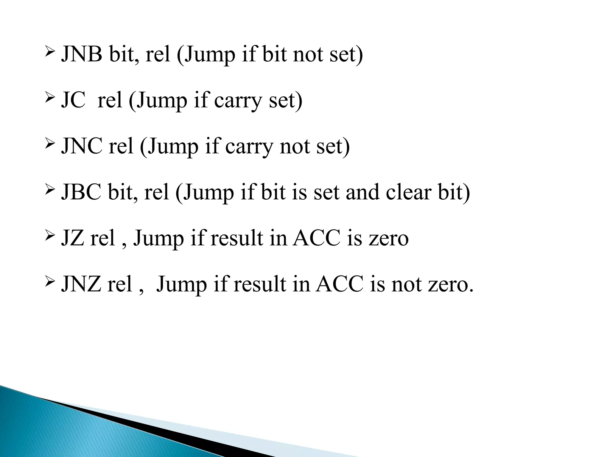
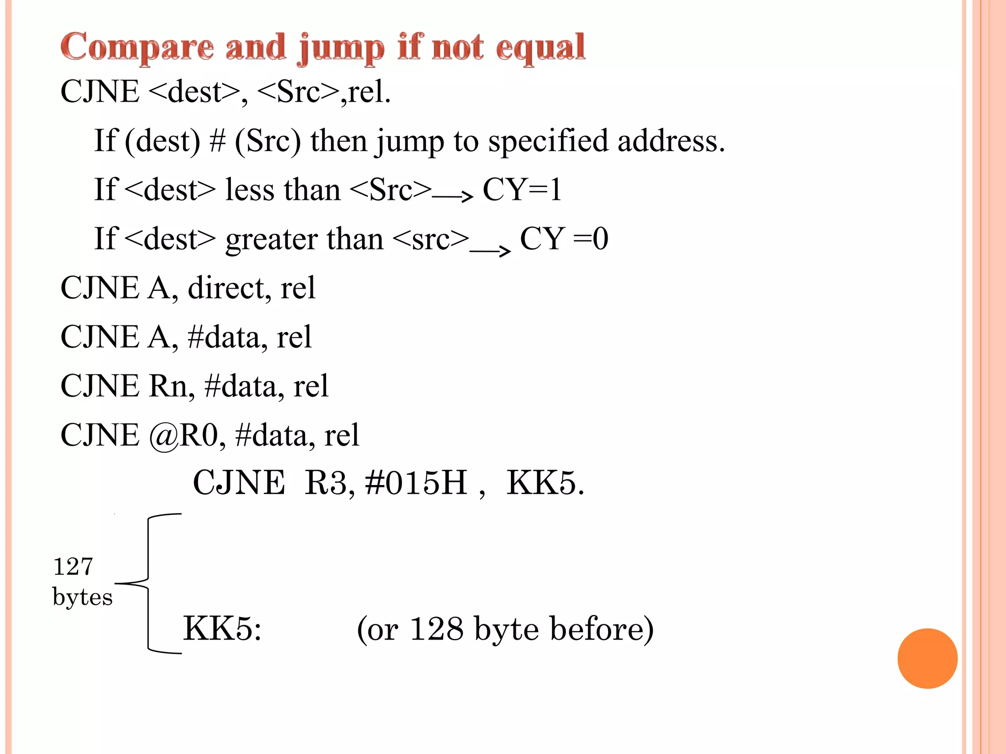
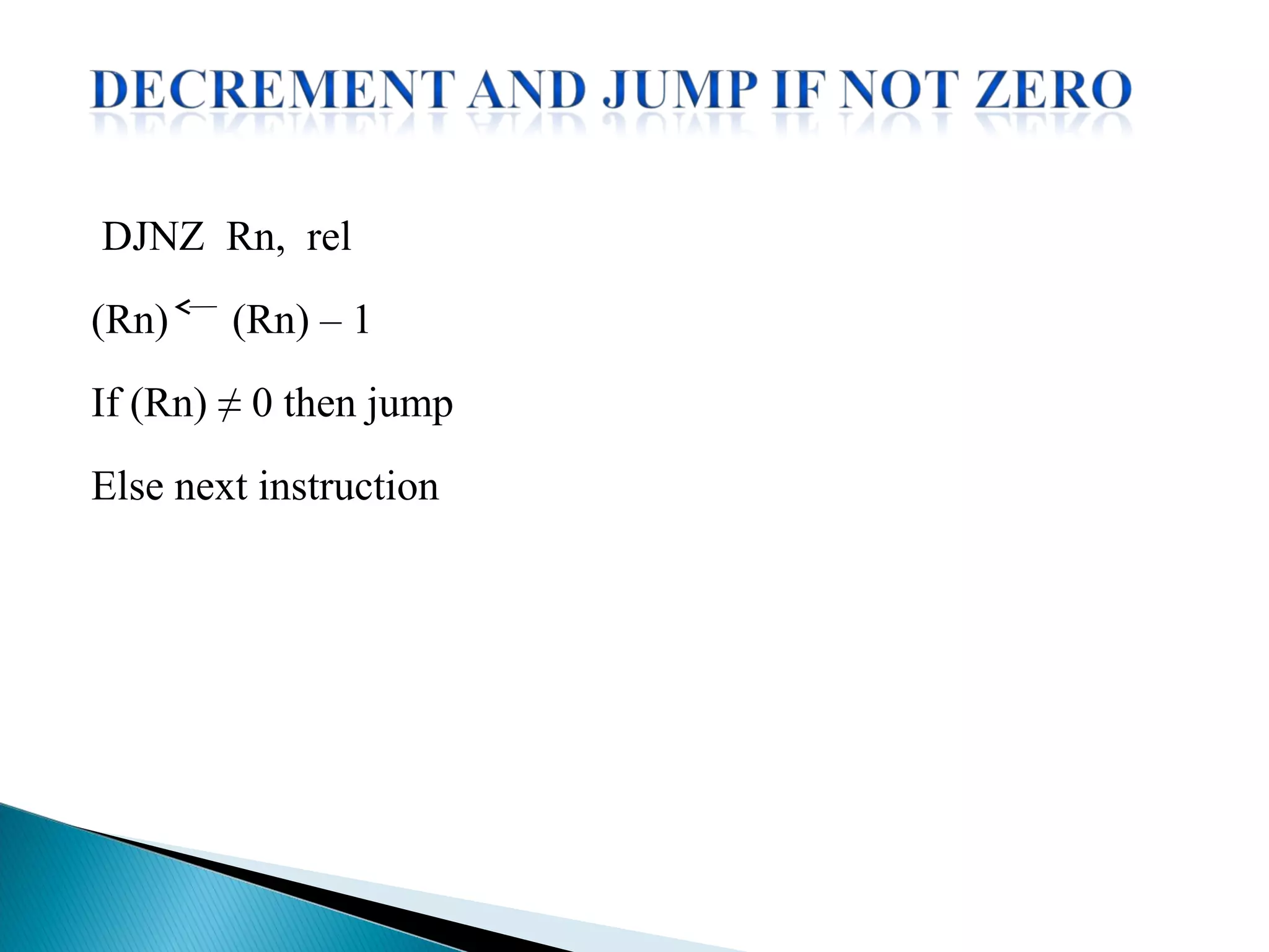
Unconditional and conditional jumps, ACALL, LCALL, and their implications in programming.
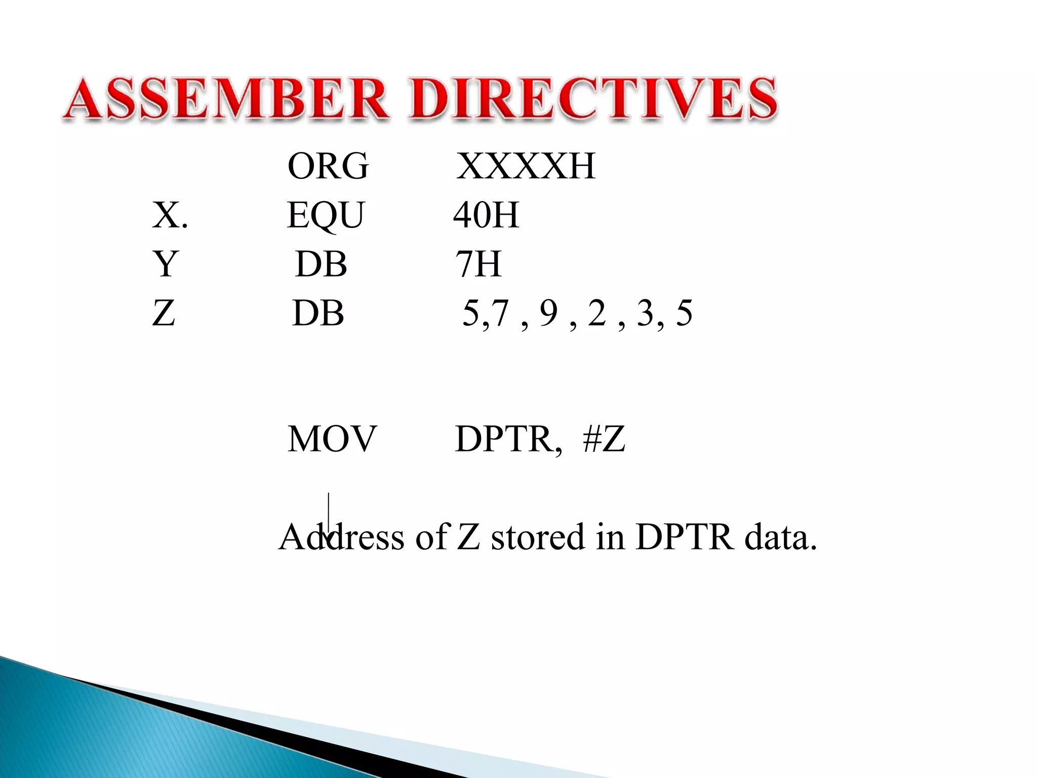
Instructions for organizing code including ORG, EQU, and defining data bytes.