Downloaded 126 times


![DECODERS: IMPLEMENTING FUNCTIONS REVISIT (1/2) Example: Implement the following function using a 3 8 decoder and appropriate logic gate f(Q,X,P) = m(0,1,4,6,7) = M(2,3,5) We may implement the function in several ways: Using a decoder with active-high outputs with an OR gate: f(Q,X,P) = m0 + m1 + m4 + m6 + m7 Using a decoder with active-low outputs with a NAND gate: f(Q,X,P) = (m0' m1' m4' m6' m7' )' Using a decoder with active-high outputs with a NOR gate: f(Q,X,P) = (m2 + m3 + m5 )' [ = M2 M3 M5 ] Using a decoder with active-low outputs with an AND gate: f(Q,X,P) = m2' m3' m5' 22](https://image.slidesharecdn.com/ch5combinattionallogic-140108074229-phpapp02/75/Logic-Design-Chapter-5-Part1-Combinattional-Logic-22-2048.jpg)


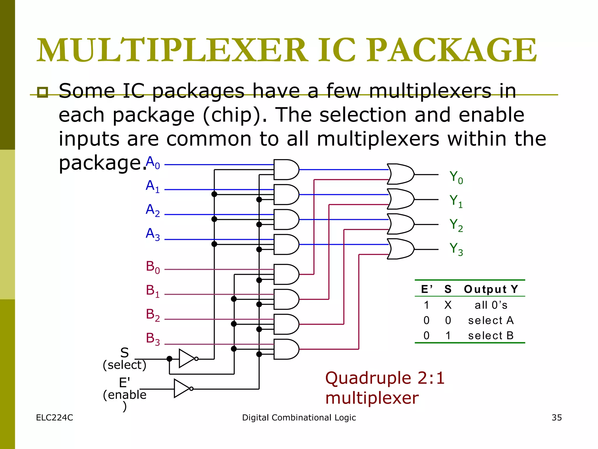


The document discusses common digital logic circuits including decoders, encoders, demultiplexers and multiplexers. It provides an overview of how these circuits work at a block level and then goes into more detail on decoders, describing their functionality, truth tables, and implementations including how to build larger decoders from smaller ones. Standard MSI decoder chips are also presented.