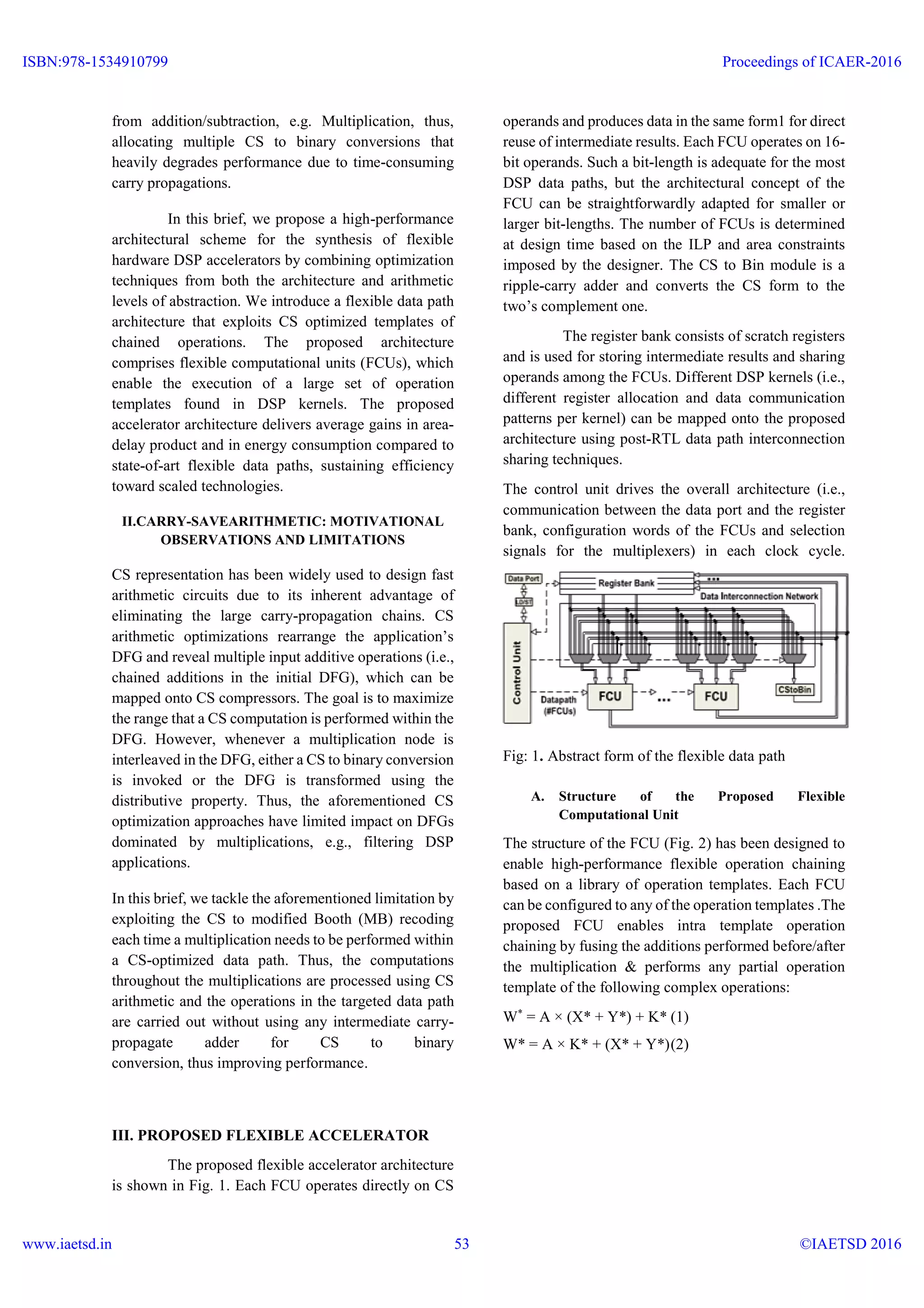
VLSI Architecture for Exploiting Carry-Save Arithmetic Using Verilog HDL Arigila venkata naveen kumar1 yachamaneni Murali2 arigilanaveen@gmail.com1 muraliy85@gmail.com2 1 PG Scholar, Dept of ECE, Audisankara College of Engineering &Technology (Autonomous), Gudur, Nellore, Andhra Pradesh. 2 Assistant professor, Dept of ECE, Audisankara College of Engineering &Technology(Autonomous), Gudur, Nellore, Andhra Pradesh ABSTRACT: Hardware acceleration has been proved an extremely promising implementation strategy for the digital signal processing (DSP) domain. Rather than adopting a monolithic application-specific integrated circuit design approach, in this brief, we present a novel accelerator architecture comprising flexible computational units that support the execution of a large set of operation templates found in DSP kernels. We differentiate from previous works on flexible accelerators by enabling computations to be aggressively performed with carry- save (CS) formatted data. Advanced arithmetic design concepts, i.e., recoding techniques, are utilized enabling CS optimizations to be performed in a larger scope than in previous approaches. Extensive experimental evaluations so what the proposed accelerator architecture delivers average gains of up to 61.91% in area-delay product and 54.43% in energy consumption compared with the state-of-art flexible data paths. Keywords: Arithmetic optimizations, carry-save (CS) form, data path synthesis, flexible accelerator, operation chaining. I. INTRODUCTION Modern embedded systems target high-end application domains requiring efficient implementations of computationally intensive digital signal processing (DSP) functions. The incorporation of heterogeneity through specialized hardware accelerators improves performance and reduces energy consumption [1]. Although application specific integrated circuits (ASICs) form the ideal acceleration solution in terms of performance and power, their inflexibility leads to increased silicon complexity, as multiple instantiated ASICs are needed to accelerate various kernels. Many researchers have proposed the use of domain-specific coarse-grained reconfigurable accelerators in order to increase ASICs’ flexibility without significantly compromising their performance High-performance flexible data paths have been proposed to efficiently map primitive or chained operations found in the initial data- flow graph (DFG) of a kernel. The templates of complex chained operations are either extracted directly from the kernel’s DFG or specified in a predefined behavioral template library. Design decisions on the accelerator’s data path highly impact its efficiency. Existing works on coarse-grained reconfigurable data paths mainly exploit architecture-level optimizations, e.g., increased instruction-level parallelism (ILP). The domain-specific architecture generation algorithms of [5] and [9] vary the type and number of computation units achieving a customized design structure. The flexible architectures were proposed exploiting ILP and operation chaining. Recently aggressive operation chaining is adopted to enable the computation of entire sub expressions using multiple ALUs with heterogeneous arithmetic features. The afore mentioned are configurable architectures exclude arithmetic Optimizations during the architectural synthesis and consider them only at the internal circuit structure of primitive components, e.g., adders, during the logic synthesis. However, research activities have shown that the arithmetic optimizations at higher abstraction levels than the structural circuit one significantly impact on the data path performance. In [10], timing-driven optimizations based on carry- save (CS) arithmetic were performed at the post- Register Transfer Level (RTL) design stage. In [11], common sub expression elimination in CS competitions is used to optimize linear DSP circuits. Verma et al. [12] developed transformation techniques on the application’s DFG to maximize the use of CS arithmetic prior the actual data path synthesis. The aforementioned CS optimization approaches target inflexible data path, i.e., ASIC, implementations. Recently, a flexible architecture combining the ILP and pipelining techniques with the CS-aware operation chaining has been proposed. However, all the aforementioned solutions feature an inherent limitation, i.e., CS optimization is bounded to merging only additions/subtractions. A CS to binary conversion is inserted before each operation that differs ISBN:978-1534910799 www.iaetsd.in Proceedings of ICAER-2016 ©IAETSD 201652
from addition/subtraction, e.g. Multiplication, thus, allocating multiple CS to binary conversions that heavily degrades performance due to time-consuming carry propagations. In this brief, we propose a high-performance architectural scheme for the synthesis of flexible hardware DSP accelerators by combining optimization techniques from both the architecture and arithmetic levels of abstraction. We introduce a flexible data path architecture that exploits CS optimized templates of chained operations. The proposed architecture comprises flexible computational units (FCUs), which enable the execution of a large set of operation templates found in DSP kernels. The proposed accelerator architecture delivers average gains in area- delay product and in energy consumption compared to state-of-art flexible data paths, sustaining efficiency toward scaled technologies. II.CARRY-SAVEARITHMETIC: MOTIVATIONAL OBSERVATIONS AND LIMITATIONS CS representation has been widely used to design fast arithmetic circuits due to its inherent advantage of eliminating the large carry-propagation chains. CS arithmetic optimizations rearrange the application’s DFG and reveal multiple input additive operations (i.e., chained additions in the initial DFG), which can be mapped onto CS compressors. The goal is to maximize the range that a CS computation is performed within the DFG. However, whenever a multiplication node is interleaved in the DFG, either a CS to binary conversion is invoked or the DFG is transformed using the distributive property. Thus, the aforementioned CS optimization approaches have limited impact on DFGs dominated by multiplications, e.g., filtering DSP applications. In this brief, we tackle the aforementioned limitation by exploiting the CS to modified Booth (MB) recoding each time a multiplication needs to be performed within a CS-optimized data path. Thus, the computations throughout the multiplications are processed using CS arithmetic and the operations in the targeted data path are carried out without using any intermediate carry- propagate adder for CS to binary conversion, thus improving performance. III. PROPOSED FLEXIBLE ACCELERATOR The proposed flexible accelerator architecture is shown in Fig. 1. Each FCU operates directly on CS operands and produces data in the same form1 for direct reuse of intermediate results. Each FCU operates on 16- bit operands. Such a bit-length is adequate for the most DSP data paths, but the architectural concept of the FCU can be straightforwardly adapted for smaller or larger bit-lengths. The number of FCUs is determined at design time based on the ILP and area constraints imposed by the designer. The CS to Bin module is a ripple-carry adder and converts the CS form to the two’s complement one. The register bank consists of scratch registers and is used for storing intermediate results and sharing operands among the FCUs. Different DSP kernels (i.e., different register allocation and data communication patterns per kernel) can be mapped onto the proposed architecture using post-RTL data path interconnection sharing techniques. The control unit drives the overall architecture (i.e., communication between the data port and the register bank, configuration words of the FCUs and selection signals for the multiplexers) in each clock cycle. Fig: 1. Abstract form of the flexible data path A. Structure of the Proposed Flexible Computational Unit The structure of the FCU (Fig. 2) has been designed to enable high-performance flexible operation chaining based on a library of operation templates. Each FCU can be configured to any of the operation templates .The proposed FCU enables intra template operation chaining by fusing the additions performed before/after the multiplication & performs any partial operation template of the following complex operations: W* = A × (X* + Y*) + K* (1) W* = A × K* + (X* + Y*)(2) ISBN:978-1534910799 www.iaetsd.in Proceedings of ICAER-2016 ©IAETSD 201653
Fig: 2. FCU The following relation holds for all CS data: X* = { XC , XS } =XC + XS . The operand A is a two’s complement number. The alternative execution paths in each FCU are specified after properly setting the control signals of the multiplexers MUX1 and MUX2 (Fig. 2). The multiplexer MUX0 outputs Y* when CL0 = 0 (i.e., X* + Y* is carried out) or Y* when X* − Y*is required and CL0 = 1. The two’s complement 4:2 CS adder produces the N* = X* + Y* when the input carry equals 0 or the N* = X* − Y*when the input carry equals 1. The MUX1 determines if N* (1) or K* (2) is multiplied with A. The MUX2 specifies if K* (1) or N*(2) is added with the multiplication product. The multiplexer MUX3 accepts the output of MUX2 and its 1’s complement and outputs the former one when an addition with the multiplication product is required (i.e., CL3 = 0) or the later one when a subtraction is carried out (i.e., CL3 = 1). The 1-bit ace for the subtraction is added in the CS adder tree. The multiplier comprises a CS-to-MB module, which adopts a recently proposed technique to recode the 17-bit P*in its respective MB digits with minimal carry propagation. The multiplier’s product consists of 17 bits. The multiplier includes a compensation method for reducing the error imposed at the product’s accuracy by the truncation technique. However, since all the FCU inputs consist of 16 bits and provided that there are no overflows, the 16 most significant bits of the 17- bit W*(i.e., the output of the Carry-Save Adder (CSA) tree, and thus, of the FCU) are inserted in the appropriate FCU when requested. B. DFG Mapping Onto the Proposed FCU-Based Architecture In order to efficiently map DSP kernels onto the proposed FCU-based accelerator, the semiautomatic synthesis methodology has been adapted. At first, a CS- aware transformation is performed onto the original DFG, merging nodes of multiple chained additions/sub- tractions to 4:2 compressors. A pattern generation on the transformed DFG clusters the CS nodes with the multiplication operations to form FCU template operations (Fig. 3). The designer selects the FCU operations covering the DFG for minimized latency. Given that the number of FCUs is fixed, a resource- constrained scheduling is considered with the available FCUs and CS to Bin modules determining the resource constraint set. The clustered DFG is scheduled, so that each FCU operation is assigned to a specific control step. A list-based scheduler has been adopted considering the mobility of FCU operations. The FCU operations are scheduled according to descending mobility. The scheduled FCU operations are bound onto FCU instances and proper configuration bits are generated. After completing register allocation, a FSM is generated in order to implement the control unit of the overall architecture. (A) (B) Fig.3. Typical chaining of addition–multiplication– addition operation (A) CS optimizations with multiplication distribution (B) incorporating the CS-to- MB recoding concept. ISBN:978-1534910799 www.iaetsd.in Proceedings of ICAER-2016 ©IAETSD 201654
IV. SIMULATION RESULTS Fig:4.RTL Fig: 5.Output Waveform V. CONCLUSION In this brief, we introduced a flexible accelerator architecture that exploits the incorporation of CS arithmetic optimizations to enable fast chaining of additive and multiplicative operations. The proposed flexible accelerator architecture is able to operate on both conventional two’s complement and CS-formatted data operands, thus enabling high degrees of computational density to be achieved. Theoretical and experimental analyses have shown that the proposed solution forms an efficient design tradeoff point delivering optimized latency/area and energy implementations. REFERENCES [1] P. Ienne and R. Leupers, Customizable Embedded Processors: Design Technologies and Applications. San Francisco, CA, USA: Morgan Kaufmann, 2007. [2] P. M. Heysters, G. J. M. Smit, and E. Molenkamp, “A flexible and energy-efficient coarse-grained reconfigurable architecture for mobile systems,” J. Super comput., vol. 26, no. 3, pp. 283–308, 2003. [3] B. Mei, S. Vernalde, D. Verkest, H. D. Man, and R. Lauwereins, “ADRES: An architecture with tightly coupled VLIW processor and coarse-grained reconfigurable matrix,” in Proc. 13th Int. Conf. Field Program. Logic Appl., vol. 2778. 2003, pp. 61–70. [4] M. D. Galanis, G. Theodoridis, S. Tragoudas, and C.E.Goutis,“A high-performance data path for synthesizing DSPkernels,”IEEETrans.Comput.-Aided Design Integr. Circuits Syst., vol. 25, no. 6, pp. 1154– 1162, Jun. 2006. [5] K. Compton and S. Hauck, “Automatic design of reconfigurable domain specific flexible cores,” IEEE Trans. Very Large Scale Integr. (VLSI)Syst., vol. 16, no. 5, pp. 493–503, May 2008. [6] S. Xydis, G. Economakos, and K. Pekmestzi, “Designing coarse-grain reconfigurable architectures by in lining flexibility into custom arithmetic data- paths,“Integr., VLSI J., vol. 42, no. 4, pp. 486–503, Sep. 2009. [7] S. Xydis, G. Economakos, D. Soudris, and K. Pekmestzi, “High performance and area efficient flexible DSP data path synthesis,” IEEE Trans.Very Large Scale Integr. (VLSI) Syst., vol. 19, no. 3, pp. 429– 442, Mar. 2011. [8] G. Ansaloni, P. Bonzini, and L. Pozzi, “EGRA: A coarse grained reconfigurable architectural template,” IEEE Trans. Very Large ScaleIntegr. (VLSI) Syst., vol. 19, no. 6, pp. 1062–1074, Jun. 2011. ISBN:978-1534910799 www.iaetsd.in Proceedings of ICAER-2016 ©IAETSD 201655
[9] M. Stojilovic, D. Novo, L. Saranovac, P. Brisk, and P.Ienne,“Selectiveflexibility: Creating domain-specific reconfigurable arrays,”IEEETrans. Comput.-Aided Design Integr. Circuits Syst., vol. 32, no.5, pp.681–694,May 2013. [10] T. Kim and J. Um, “A practical approach to the synthesis of arithmetic circuits using carry-save- adders,” IEEE Trans. Comput.-Aided Design Integr. CircuitsSyst., vol.19, no.5, pp.615–624,May 2000. [11] A. Hosangadi, F. Fallah, and R. Kastner, “Optimizinghighspeedarithmetic circuits using three- terme xtraction,” in Proc. Design,Autom.Test Eur. (DATE), vol. 1. Mar. 2006, pp. 1–6. [12] A. K. Verma, P. Brisk, and P. Ienne, “Data-flow transformations to maximize the use of carry-save representation in arithmetic circuits,” IEEE Trans. Comput.-Aided Design Integr. Circuits Syst., vol. 27, no. 10, pp. 1761–1774, Oct. 2008. BIOGRAPHIES: Arigila venkata naveen Kumar is currently a PG scholar of VLSI in Audisankara College of Engineering and Technology (Autonomous). He received B.TECH degree from JNTU. His current research interest includes Analysis &VLSI System Design Ph.: 9493012315 Yachamaneni Murali Currently working as Assistant Professor Department of Electronics and Communication engineering in Audisankara College of Engineering and technology (Autonomous),Gudur, Nellore, Andhra Pradesh His current research interest includes VLSI design ISBN:978-1534910799 www.iaetsd.in Proceedings of ICAER-2016 ©IAETSD 201656

Iaetsd vlsi architecture for exploiting carry save arithmetic using verilog hdl

  • 1.
    VLSI Architecture forExploiting Carry-Save Arithmetic Using Verilog HDL Arigila venkata naveen kumar1 yachamaneni Murali2 arigilanaveen@gmail.com1 muraliy85@gmail.com2 1 PG Scholar, Dept of ECE, Audisankara College of Engineering &Technology (Autonomous), Gudur, Nellore, Andhra Pradesh. 2 Assistant professor, Dept of ECE, Audisankara College of Engineering &Technology(Autonomous), Gudur, Nellore, Andhra Pradesh ABSTRACT: Hardware acceleration has been proved an extremely promising implementation strategy for the digital signal processing (DSP) domain. Rather than adopting a monolithic application-specific integrated circuit design approach, in this brief, we present a novel accelerator architecture comprising flexible computational units that support the execution of a large set of operation templates found in DSP kernels. We differentiate from previous works on flexible accelerators by enabling computations to be aggressively performed with carry- save (CS) formatted data. Advanced arithmetic design concepts, i.e., recoding techniques, are utilized enabling CS optimizations to be performed in a larger scope than in previous approaches. Extensive experimental evaluations so what the proposed accelerator architecture delivers average gains of up to 61.91% in area-delay product and 54.43% in energy consumption compared with the state-of-art flexible data paths. Keywords: Arithmetic optimizations, carry-save (CS) form, data path synthesis, flexible accelerator, operation chaining. I. INTRODUCTION Modern embedded systems target high-end application domains requiring efficient implementations of computationally intensive digital signal processing (DSP) functions. The incorporation of heterogeneity through specialized hardware accelerators improves performance and reduces energy consumption [1]. Although application specific integrated circuits (ASICs) form the ideal acceleration solution in terms of performance and power, their inflexibility leads to increased silicon complexity, as multiple instantiated ASICs are needed to accelerate various kernels. Many researchers have proposed the use of domain-specific coarse-grained reconfigurable accelerators in order to increase ASICs’ flexibility without significantly compromising their performance High-performance flexible data paths have been proposed to efficiently map primitive or chained operations found in the initial data- flow graph (DFG) of a kernel. The templates of complex chained operations are either extracted directly from the kernel’s DFG or specified in a predefined behavioral template library. Design decisions on the accelerator’s data path highly impact its efficiency. Existing works on coarse-grained reconfigurable data paths mainly exploit architecture-level optimizations, e.g., increased instruction-level parallelism (ILP). The domain-specific architecture generation algorithms of [5] and [9] vary the type and number of computation units achieving a customized design structure. The flexible architectures were proposed exploiting ILP and operation chaining. Recently aggressive operation chaining is adopted to enable the computation of entire sub expressions using multiple ALUs with heterogeneous arithmetic features. The afore mentioned are configurable architectures exclude arithmetic Optimizations during the architectural synthesis and consider them only at the internal circuit structure of primitive components, e.g., adders, during the logic synthesis. However, research activities have shown that the arithmetic optimizations at higher abstraction levels than the structural circuit one significantly impact on the data path performance. In [10], timing-driven optimizations based on carry- save (CS) arithmetic were performed at the post- Register Transfer Level (RTL) design stage. In [11], common sub expression elimination in CS competitions is used to optimize linear DSP circuits. Verma et al. [12] developed transformation techniques on the application’s DFG to maximize the use of CS arithmetic prior the actual data path synthesis. The aforementioned CS optimization approaches target inflexible data path, i.e., ASIC, implementations. Recently, a flexible architecture combining the ILP and pipelining techniques with the CS-aware operation chaining has been proposed. However, all the aforementioned solutions feature an inherent limitation, i.e., CS optimization is bounded to merging only additions/subtractions. A CS to binary conversion is inserted before each operation that differs ISBN:978-1534910799 www.iaetsd.in Proceedings of ICAER-2016 ©IAETSD 201652
  • 2.
    from addition/subtraction, e.g.Multiplication, thus, allocating multiple CS to binary conversions that heavily degrades performance due to time-consuming carry propagations. In this brief, we propose a high-performance architectural scheme for the synthesis of flexible hardware DSP accelerators by combining optimization techniques from both the architecture and arithmetic levels of abstraction. We introduce a flexible data path architecture that exploits CS optimized templates of chained operations. The proposed architecture comprises flexible computational units (FCUs), which enable the execution of a large set of operation templates found in DSP kernels. The proposed accelerator architecture delivers average gains in area- delay product and in energy consumption compared to state-of-art flexible data paths, sustaining efficiency toward scaled technologies. II.CARRY-SAVEARITHMETIC: MOTIVATIONAL OBSERVATIONS AND LIMITATIONS CS representation has been widely used to design fast arithmetic circuits due to its inherent advantage of eliminating the large carry-propagation chains. CS arithmetic optimizations rearrange the application’s DFG and reveal multiple input additive operations (i.e., chained additions in the initial DFG), which can be mapped onto CS compressors. The goal is to maximize the range that a CS computation is performed within the DFG. However, whenever a multiplication node is interleaved in the DFG, either a CS to binary conversion is invoked or the DFG is transformed using the distributive property. Thus, the aforementioned CS optimization approaches have limited impact on DFGs dominated by multiplications, e.g., filtering DSP applications. In this brief, we tackle the aforementioned limitation by exploiting the CS to modified Booth (MB) recoding each time a multiplication needs to be performed within a CS-optimized data path. Thus, the computations throughout the multiplications are processed using CS arithmetic and the operations in the targeted data path are carried out without using any intermediate carry- propagate adder for CS to binary conversion, thus improving performance. III. PROPOSED FLEXIBLE ACCELERATOR The proposed flexible accelerator architecture is shown in Fig. 1. Each FCU operates directly on CS operands and produces data in the same form1 for direct reuse of intermediate results. Each FCU operates on 16- bit operands. Such a bit-length is adequate for the most DSP data paths, but the architectural concept of the FCU can be straightforwardly adapted for smaller or larger bit-lengths. The number of FCUs is determined at design time based on the ILP and area constraints imposed by the designer. The CS to Bin module is a ripple-carry adder and converts the CS form to the two’s complement one. The register bank consists of scratch registers and is used for storing intermediate results and sharing operands among the FCUs. Different DSP kernels (i.e., different register allocation and data communication patterns per kernel) can be mapped onto the proposed architecture using post-RTL data path interconnection sharing techniques. The control unit drives the overall architecture (i.e., communication between the data port and the register bank, configuration words of the FCUs and selection signals for the multiplexers) in each clock cycle. Fig: 1. Abstract form of the flexible data path A. Structure of the Proposed Flexible Computational Unit The structure of the FCU (Fig. 2) has been designed to enable high-performance flexible operation chaining based on a library of operation templates. Each FCU can be configured to any of the operation templates .The proposed FCU enables intra template operation chaining by fusing the additions performed before/after the multiplication & performs any partial operation template of the following complex operations: W* = A × (X* + Y*) + K* (1) W* = A × K* + (X* + Y*)(2) ISBN:978-1534910799 www.iaetsd.in Proceedings of ICAER-2016 ©IAETSD 201653
  • 3.
    Fig: 2. FCU Thefollowing relation holds for all CS data: X* = { XC , XS } =XC + XS . The operand A is a two’s complement number. The alternative execution paths in each FCU are specified after properly setting the control signals of the multiplexers MUX1 and MUX2 (Fig. 2). The multiplexer MUX0 outputs Y* when CL0 = 0 (i.e., X* + Y* is carried out) or Y* when X* − Y*is required and CL0 = 1. The two’s complement 4:2 CS adder produces the N* = X* + Y* when the input carry equals 0 or the N* = X* − Y*when the input carry equals 1. The MUX1 determines if N* (1) or K* (2) is multiplied with A. The MUX2 specifies if K* (1) or N*(2) is added with the multiplication product. The multiplexer MUX3 accepts the output of MUX2 and its 1’s complement and outputs the former one when an addition with the multiplication product is required (i.e., CL3 = 0) or the later one when a subtraction is carried out (i.e., CL3 = 1). The 1-bit ace for the subtraction is added in the CS adder tree. The multiplier comprises a CS-to-MB module, which adopts a recently proposed technique to recode the 17-bit P*in its respective MB digits with minimal carry propagation. The multiplier’s product consists of 17 bits. The multiplier includes a compensation method for reducing the error imposed at the product’s accuracy by the truncation technique. However, since all the FCU inputs consist of 16 bits and provided that there are no overflows, the 16 most significant bits of the 17- bit W*(i.e., the output of the Carry-Save Adder (CSA) tree, and thus, of the FCU) are inserted in the appropriate FCU when requested. B. DFG Mapping Onto the Proposed FCU-Based Architecture In order to efficiently map DSP kernels onto the proposed FCU-based accelerator, the semiautomatic synthesis methodology has been adapted. At first, a CS- aware transformation is performed onto the original DFG, merging nodes of multiple chained additions/sub- tractions to 4:2 compressors. A pattern generation on the transformed DFG clusters the CS nodes with the multiplication operations to form FCU template operations (Fig. 3). The designer selects the FCU operations covering the DFG for minimized latency. Given that the number of FCUs is fixed, a resource- constrained scheduling is considered with the available FCUs and CS to Bin modules determining the resource constraint set. The clustered DFG is scheduled, so that each FCU operation is assigned to a specific control step. A list-based scheduler has been adopted considering the mobility of FCU operations. The FCU operations are scheduled according to descending mobility. The scheduled FCU operations are bound onto FCU instances and proper configuration bits are generated. After completing register allocation, a FSM is generated in order to implement the control unit of the overall architecture. (A) (B) Fig.3. Typical chaining of addition–multiplication– addition operation (A) CS optimizations with multiplication distribution (B) incorporating the CS-to- MB recoding concept. ISBN:978-1534910799 www.iaetsd.in Proceedings of ICAER-2016 ©IAETSD 201654
  • 4.
    IV. SIMULATION RESULTS Fig:4.RTL Fig:5.Output Waveform V. CONCLUSION In this brief, we introduced a flexible accelerator architecture that exploits the incorporation of CS arithmetic optimizations to enable fast chaining of additive and multiplicative operations. The proposed flexible accelerator architecture is able to operate on both conventional two’s complement and CS-formatted data operands, thus enabling high degrees of computational density to be achieved. Theoretical and experimental analyses have shown that the proposed solution forms an efficient design tradeoff point delivering optimized latency/area and energy implementations. REFERENCES [1] P. Ienne and R. Leupers, Customizable Embedded Processors: Design Technologies and Applications. San Francisco, CA, USA: Morgan Kaufmann, 2007. [2] P. M. Heysters, G. J. M. Smit, and E. Molenkamp, “A flexible and energy-efficient coarse-grained reconfigurable architecture for mobile systems,” J. Super comput., vol. 26, no. 3, pp. 283–308, 2003. [3] B. Mei, S. Vernalde, D. Verkest, H. D. Man, and R. Lauwereins, “ADRES: An architecture with tightly coupled VLIW processor and coarse-grained reconfigurable matrix,” in Proc. 13th Int. Conf. Field Program. Logic Appl., vol. 2778. 2003, pp. 61–70. [4] M. D. Galanis, G. Theodoridis, S. Tragoudas, and C.E.Goutis,“A high-performance data path for synthesizing DSPkernels,”IEEETrans.Comput.-Aided Design Integr. Circuits Syst., vol. 25, no. 6, pp. 1154– 1162, Jun. 2006. [5] K. Compton and S. Hauck, “Automatic design of reconfigurable domain specific flexible cores,” IEEE Trans. Very Large Scale Integr. (VLSI)Syst., vol. 16, no. 5, pp. 493–503, May 2008. [6] S. Xydis, G. Economakos, and K. Pekmestzi, “Designing coarse-grain reconfigurable architectures by in lining flexibility into custom arithmetic data- paths,“Integr., VLSI J., vol. 42, no. 4, pp. 486–503, Sep. 2009. [7] S. Xydis, G. Economakos, D. Soudris, and K. Pekmestzi, “High performance and area efficient flexible DSP data path synthesis,” IEEE Trans.Very Large Scale Integr. (VLSI) Syst., vol. 19, no. 3, pp. 429– 442, Mar. 2011. [8] G. Ansaloni, P. Bonzini, and L. Pozzi, “EGRA: A coarse grained reconfigurable architectural template,” IEEE Trans. Very Large ScaleIntegr. (VLSI) Syst., vol. 19, no. 6, pp. 1062–1074, Jun. 2011. ISBN:978-1534910799 www.iaetsd.in Proceedings of ICAER-2016 ©IAETSD 201655
  • 5.
    [9] M. Stojilovic,D. Novo, L. Saranovac, P. Brisk, and P.Ienne,“Selectiveflexibility: Creating domain-specific reconfigurable arrays,”IEEETrans. Comput.-Aided Design Integr. Circuits Syst., vol. 32, no.5, pp.681–694,May 2013. [10] T. Kim and J. Um, “A practical approach to the synthesis of arithmetic circuits using carry-save- adders,” IEEE Trans. Comput.-Aided Design Integr. CircuitsSyst., vol.19, no.5, pp.615–624,May 2000. [11] A. Hosangadi, F. Fallah, and R. Kastner, “Optimizinghighspeedarithmetic circuits using three- terme xtraction,” in Proc. Design,Autom.Test Eur. (DATE), vol. 1. Mar. 2006, pp. 1–6. [12] A. K. Verma, P. Brisk, and P. Ienne, “Data-flow transformations to maximize the use of carry-save representation in arithmetic circuits,” IEEE Trans. Comput.-Aided Design Integr. Circuits Syst., vol. 27, no. 10, pp. 1761–1774, Oct. 2008. BIOGRAPHIES: Arigila venkata naveen Kumar is currently a PG scholar of VLSI in Audisankara College of Engineering and Technology (Autonomous). He received B.TECH degree from JNTU. His current research interest includes Analysis &VLSI System Design Ph.: 9493012315 Yachamaneni Murali Currently working as Assistant Professor Department of Electronics and Communication engineering in Audisankara College of Engineering and technology (Autonomous),Gudur, Nellore, Andhra Pradesh His current research interest includes VLSI design ISBN:978-1534910799 www.iaetsd.in Proceedings of ICAER-2016 ©IAETSD 201656