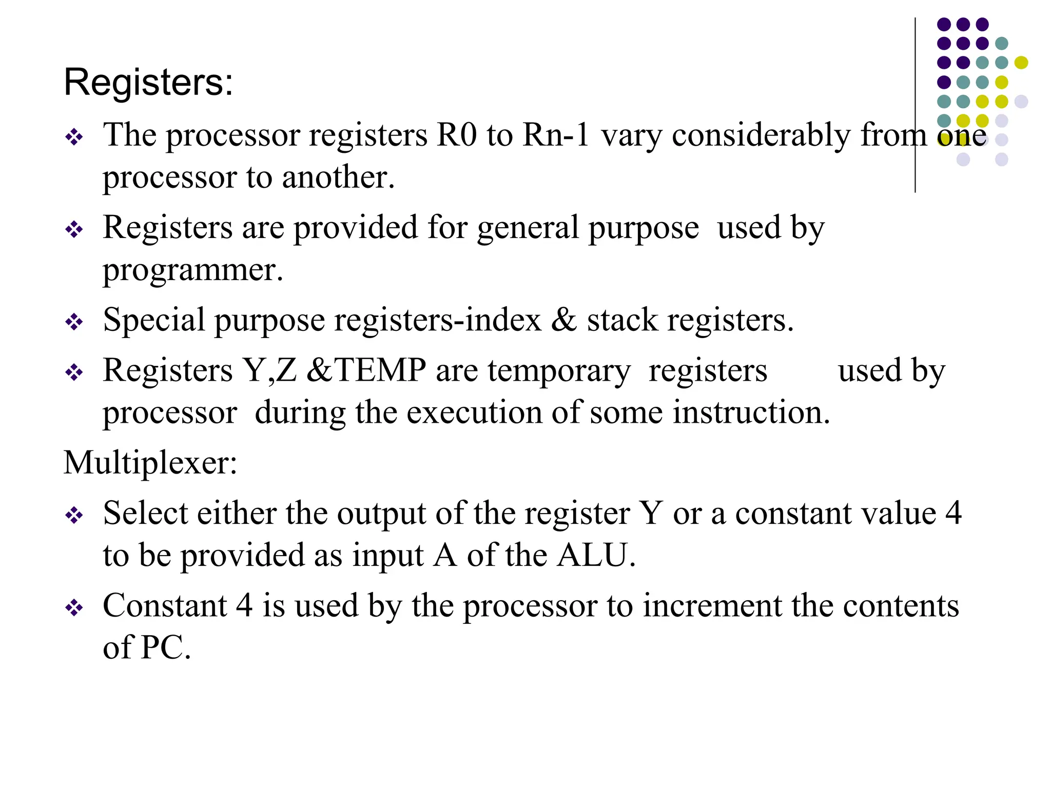
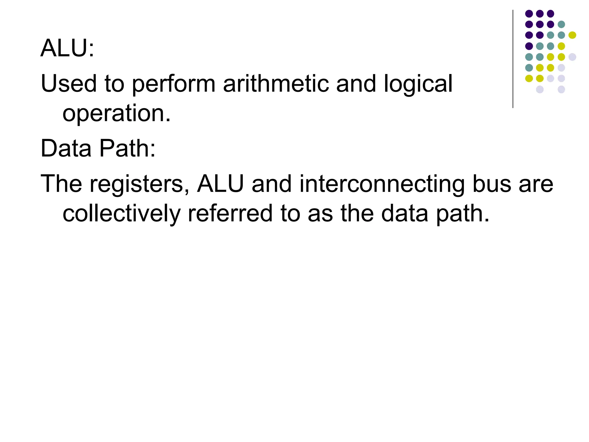
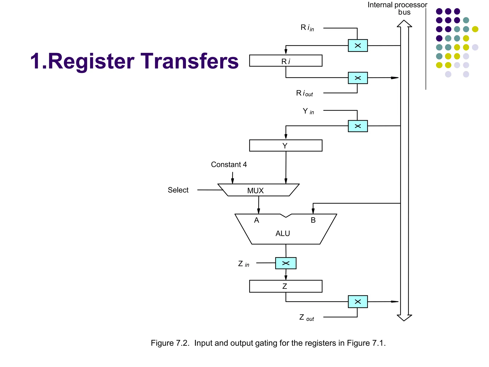
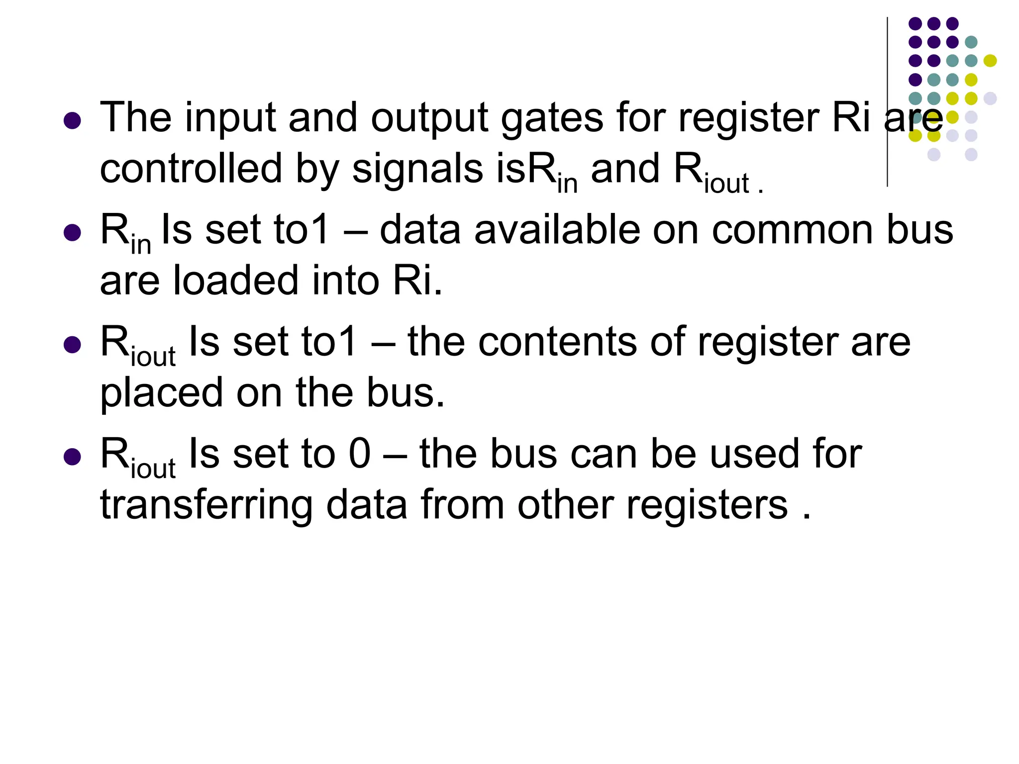
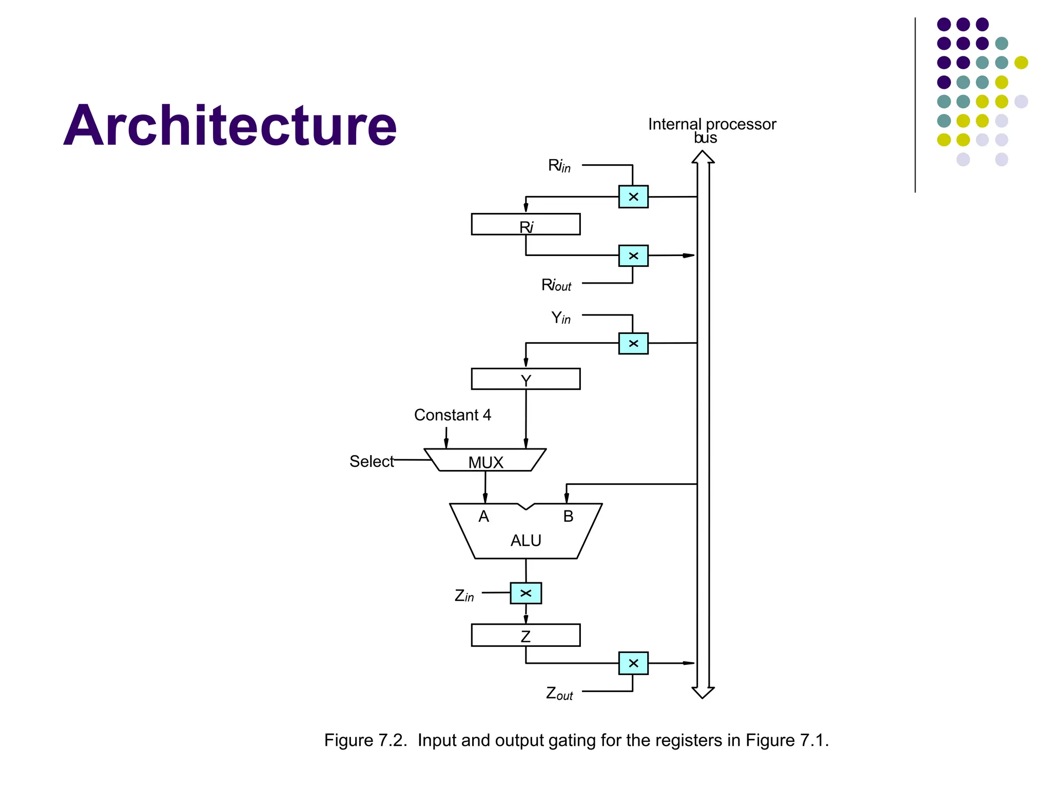
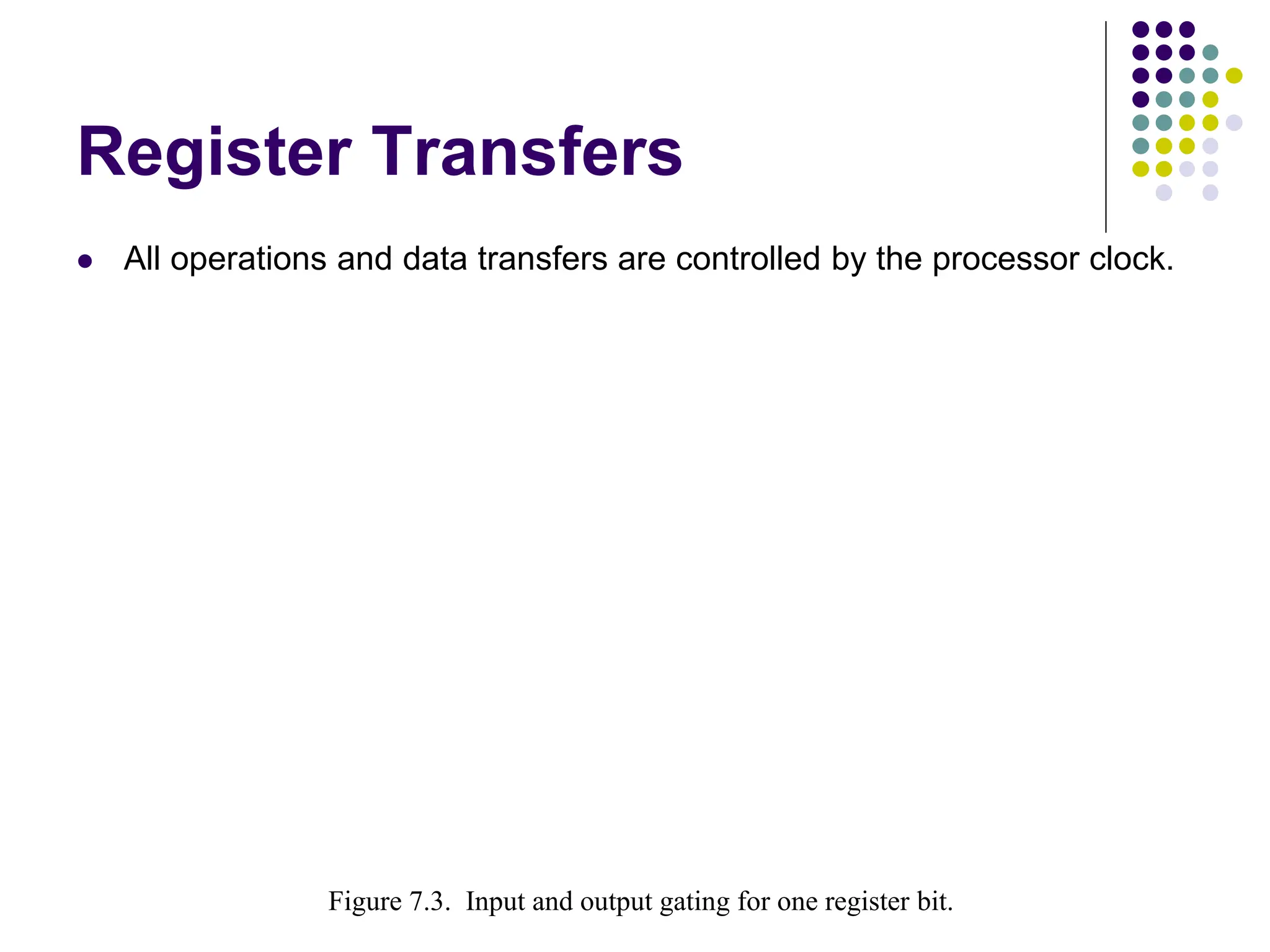
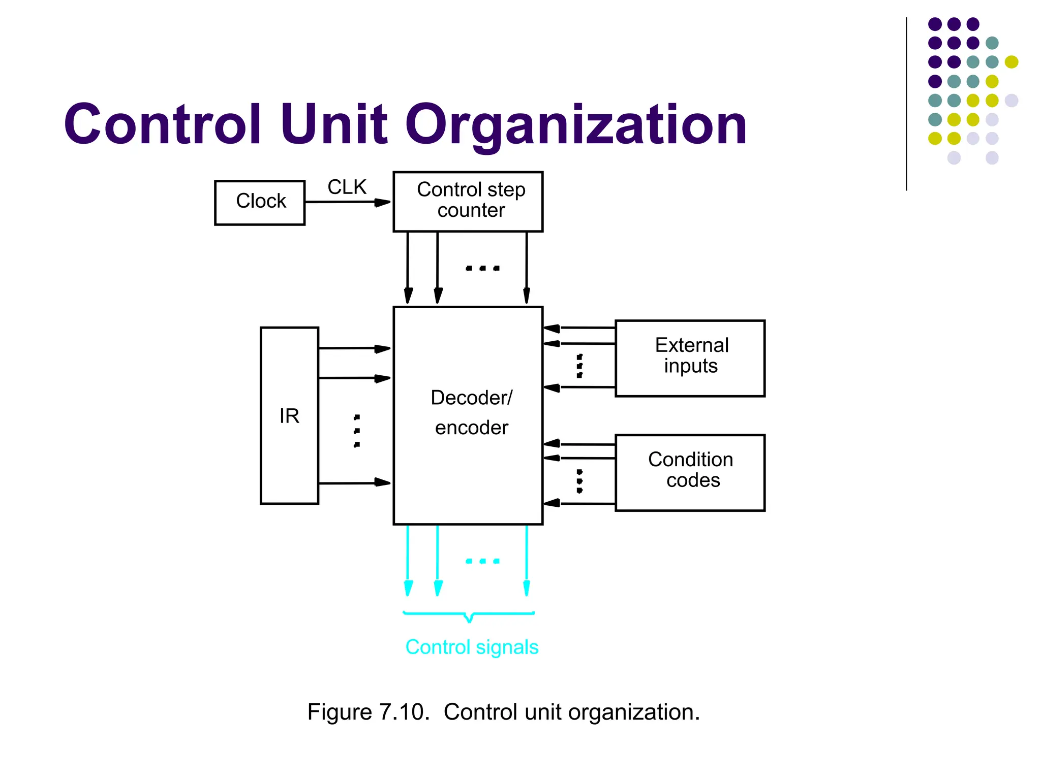
The document discusses the basic components and organization of an instruction set processor (ISP). It describes: 1. The fundamental components of an ISP including the program counter (PC), instruction register (IR), memory, registers, arithmetic logic unit (ALU), and their interconnections via a bus. 2. How an instruction is executed through fetching from memory, decoding, executing arithmetic/logical operations, and storing results. 3. The role of control signals in coordinating data movement between components and executing instructions in sequential steps. Control is implemented through hardwired digital logic circuits.

![Executing an Instruction Fetch the contents of the memory location pointed to by the PC. The contents of this location are loaded into the IR (fetch phase). IR ← [[PC]] Assuming that the memory is byte addressable, increment the contents of the PC by 4 (fetch phase). PC ← [PC] + 4 Carry out the actions specified by the instruction in the IR (execution phase).](https://image.slidesharecdn.com/unit6-basic-processing-unit-240210094253-a07f9ab0/75/basic-processing-unit-computer-organ-ppt-5-2048.jpg)

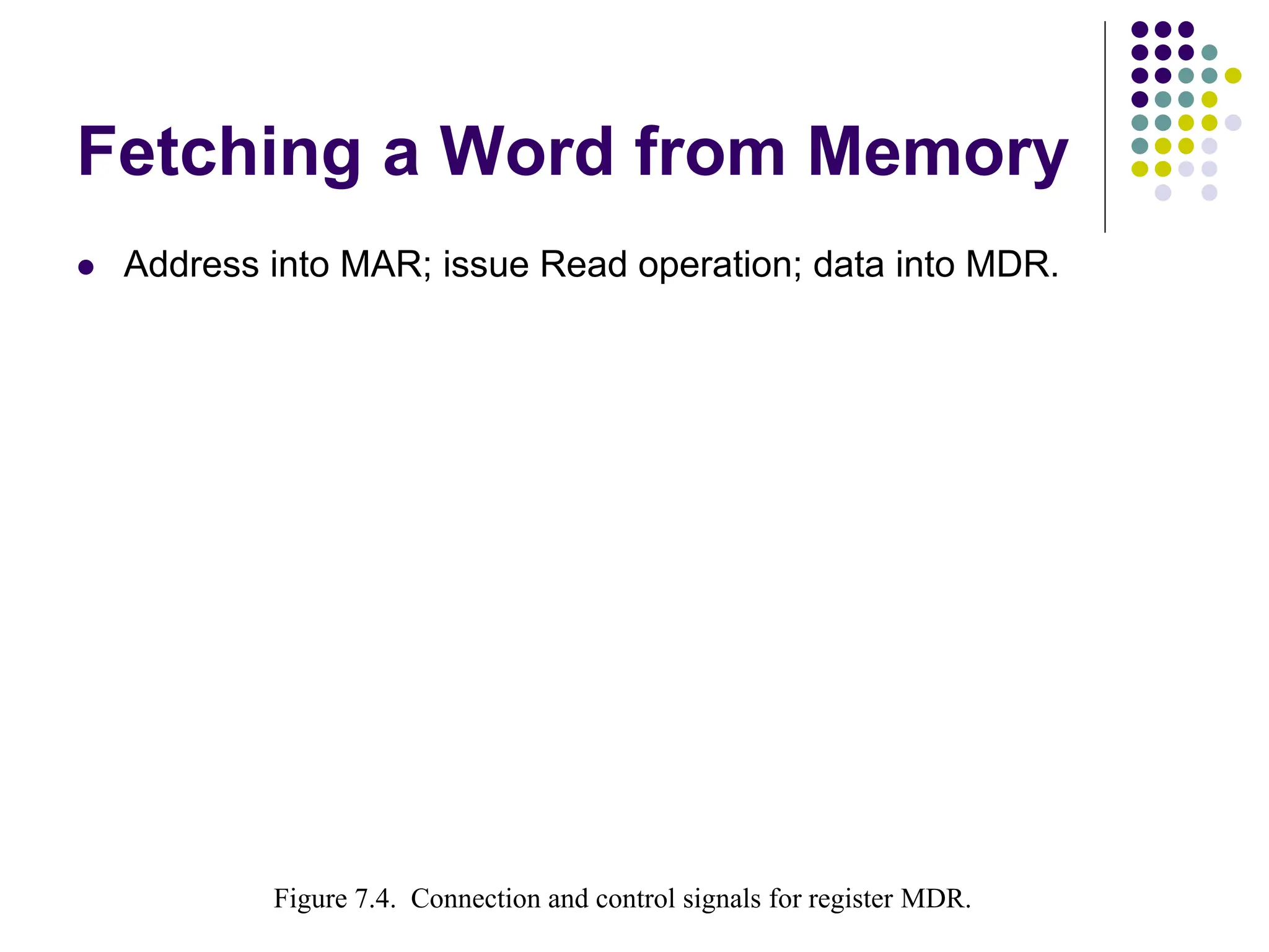
![3.Fetching a Word from Memory The response time of each memory access varies (cache miss, memory-mapped I/O,…). To accommodate this, the processor waits until it receives an indication that the requested operation has been completed (Memory-Function-Completed, MFC). Move (R1), R2 MAR ← [R1] Start a Read operation on the memory bus Wait for the MFC response from the memory Load MDR from the memory bus R2 ← [MDR]](https://image.slidesharecdn.com/unit6-basic-processing-unit-240210094253-a07f9ab0/75/basic-processing-unit-computer-organ-ppt-19-2048.jpg)


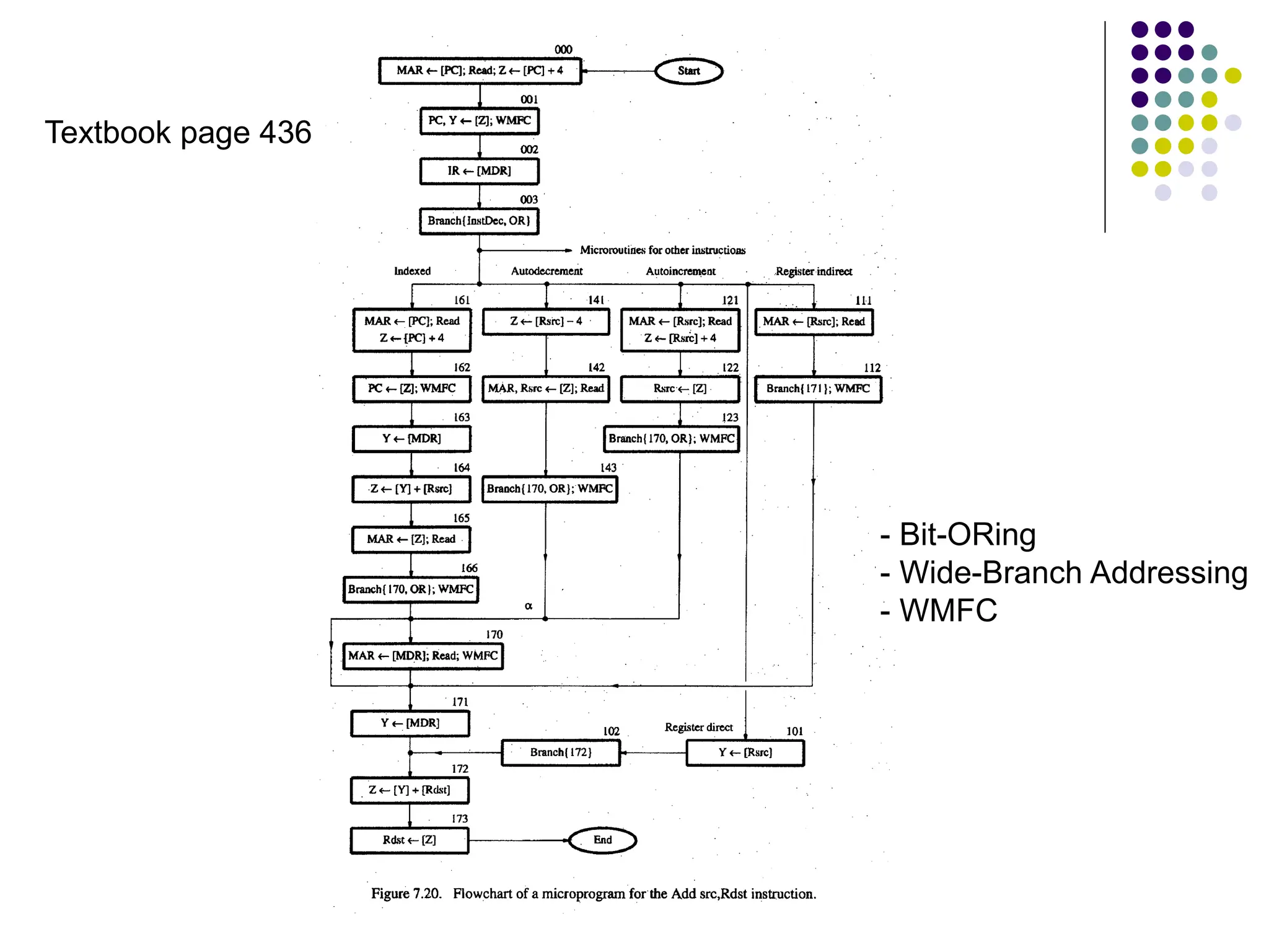
![OP code 0 1 0 Rsrc Rdst Mode Contents of IR 0 3 4 7 8 10 11 Figure 7.21. Microinstruction for Add (Rsrc)+,Rdst. Note:Microinstruction at location 170 is not executed for this addressing mode. Address Microinstruction (octal) 000 PC out, MARin, Read, Select 4, Add, Zin 001 Zout, PC in, Yin, WMFC 002 MDRout, IRin 003 Branch { PC 101 (from Instruction decoder); PC 5,4 [IR10,9 ]; PC 3 121 Rsrc out, MARin, Read, Select4, Add, Z in 122 Zout, Rsrc in 123 170 MDRout, MARin, Read, WMFC 171 MDRout, Yin 172 Rdst out, SelectY , Add, Zin 173 Zout, Rdst in, End [IR10] [IR9] [IR8]} Branch { PC 170;PC 0 [IR8]}, WMFC Textbook page 439](https://image.slidesharecdn.com/unit6-basic-processing-unit-240210094253-a07f9ab0/75/basic-processing-unit-computer-organ-ppt-50-2048.jpg)