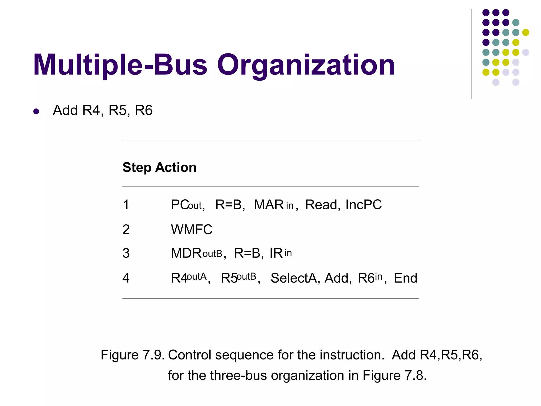
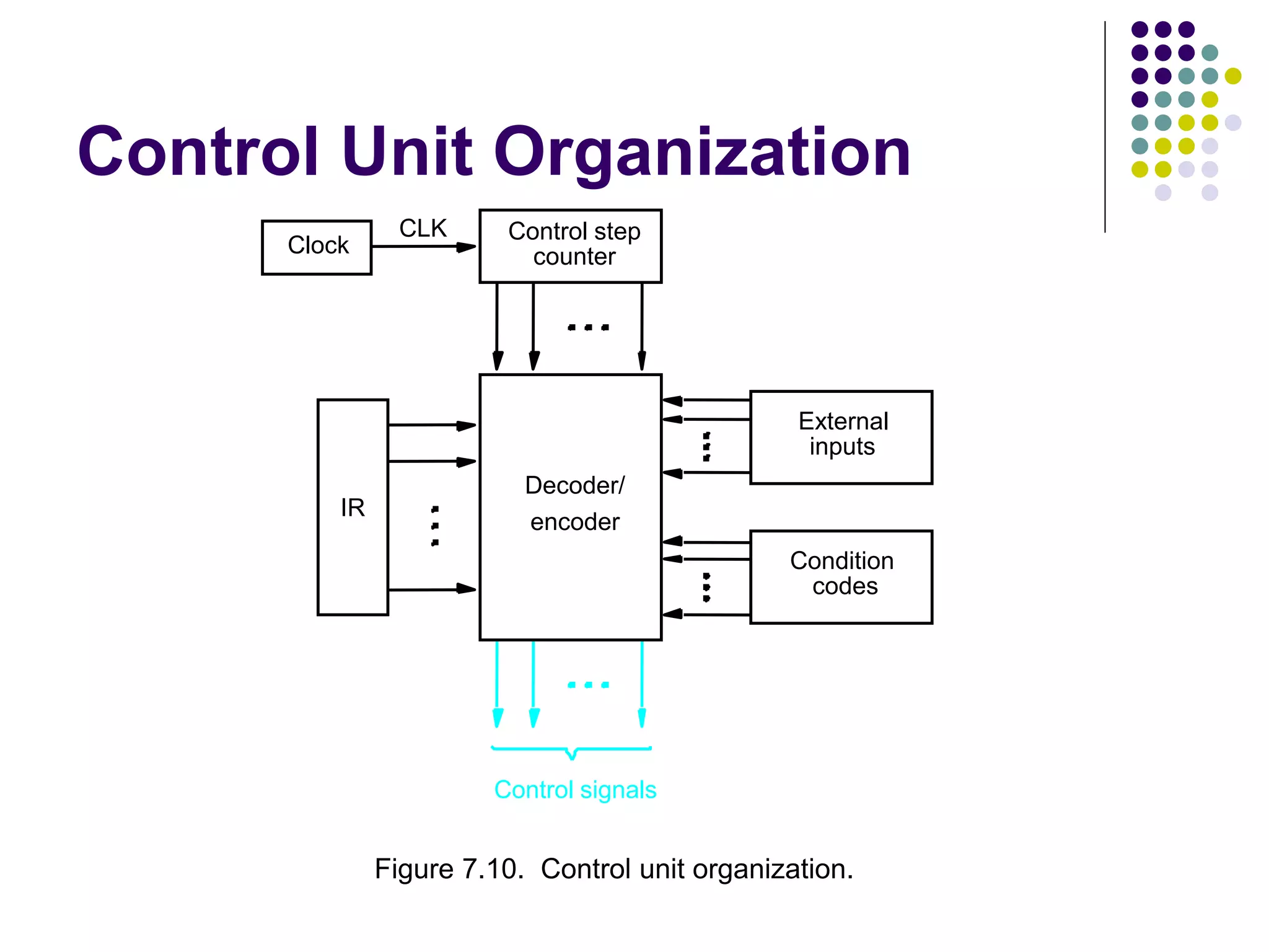
The document describes the basic processing unit of a computer. It discusses how a processor fetches and executes instructions through a series of steps. It explains the components involved, such as the program counter, instruction register, and arithmetic logic unit. It also covers different organizations for controlling instruction execution, including hardwired control and microprogrammed control using microinstructions and a control store.

![Executing an Instruction Fetch the contents of the memory location pointed to by the PC. The contents of this location are loaded into the IR (fetch phase). IR ← [[PC]] Assuming that the memory is byte addressable, increment the contents of the PC by 4 (fetch phase). PC ← [PC] + 4 Carry out the actions specified by the instruction in the IR (execution phase).](https://image.slidesharecdn.com/chapter3-basicprocessingunit-230401033245-413b61f8/75/chapter3-Basic-Processing-Unit-ppt-5-2048.jpg)
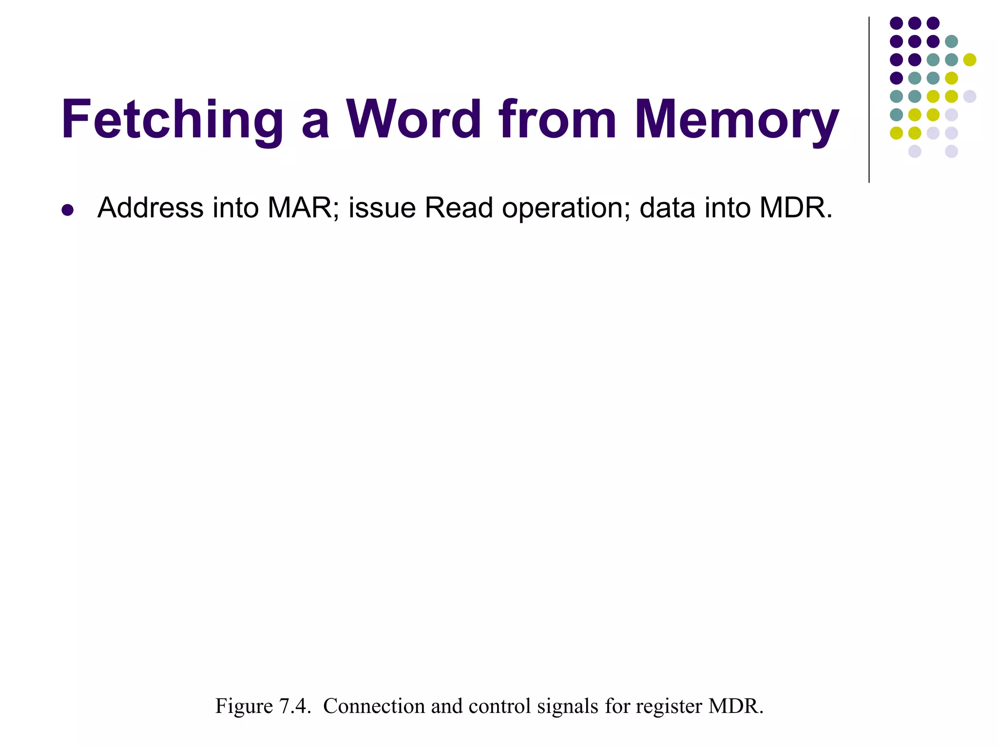
![Fetching a Word from Memory The response time of each memory access varies (cache miss, memory-mapped I/O,…). To accommodate this, the processor waits until it receives an indication that the requested operation has been completed (Memory-Function-Completed, MFC). Move (R1), R2 MAR ← [R1] Start a Read operation on the memory bus Wait for the MFC response from the memory Load MDR from the memory bus R2 ← [MDR]](https://image.slidesharecdn.com/chapter3-basicprocessingunit-230401033245-413b61f8/75/chapter3-Basic-Processing-Unit-ppt-12-2048.jpg)
![Timing Figure 7.5. Timing of a memory Read operation. MFC MDRout Assume MAR is always available on the address lines of the memory bus. R2 ← [MDR] MAR ← [R1] Start a Read operation on the memory bus Wait for the MFC response from the memory Load MDR from the memory bus](https://image.slidesharecdn.com/chapter3-basicprocessingunit-230401033245-413b61f8/75/chapter3-Basic-Processing-Unit-ppt-13-2048.jpg)


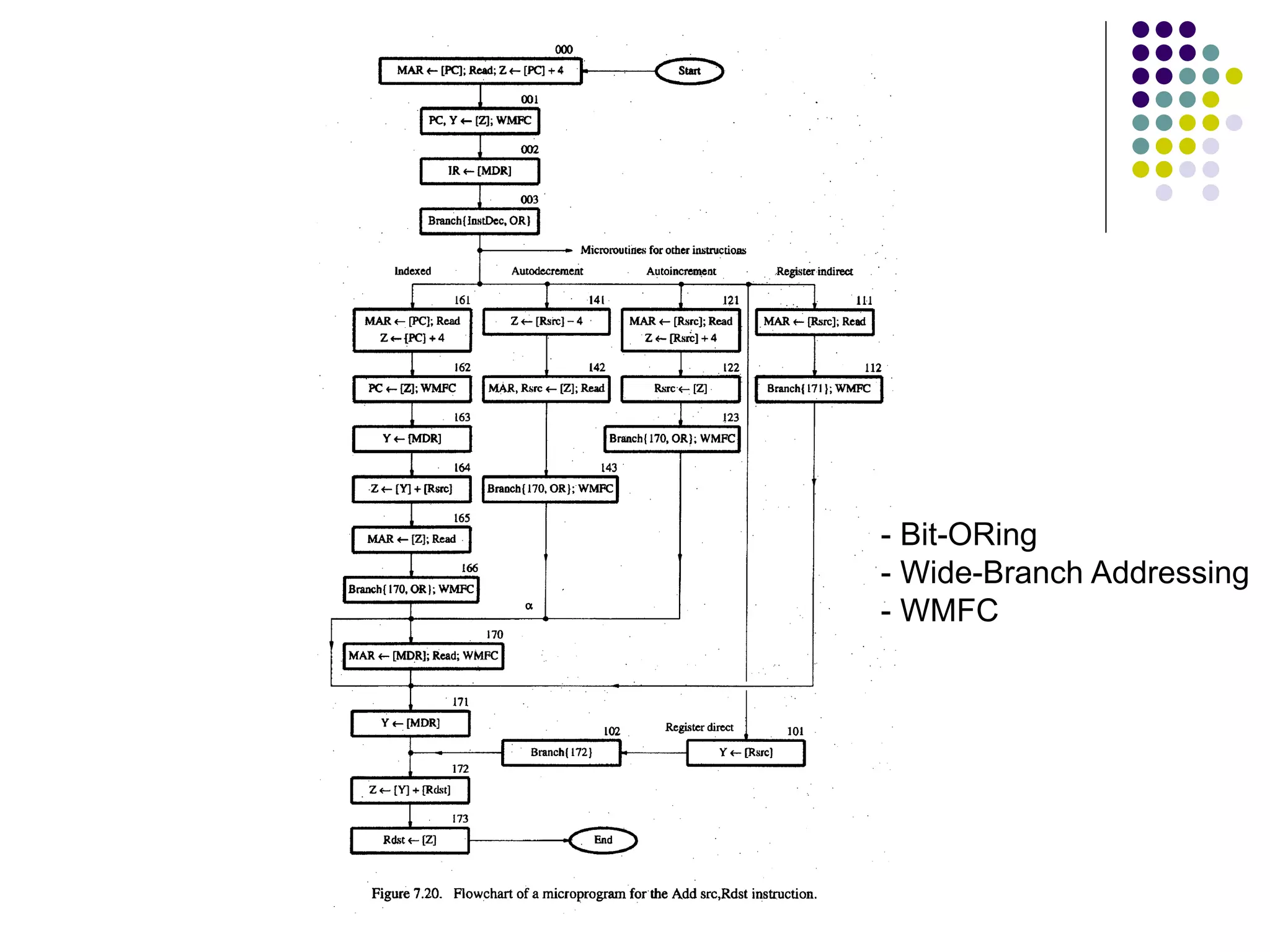
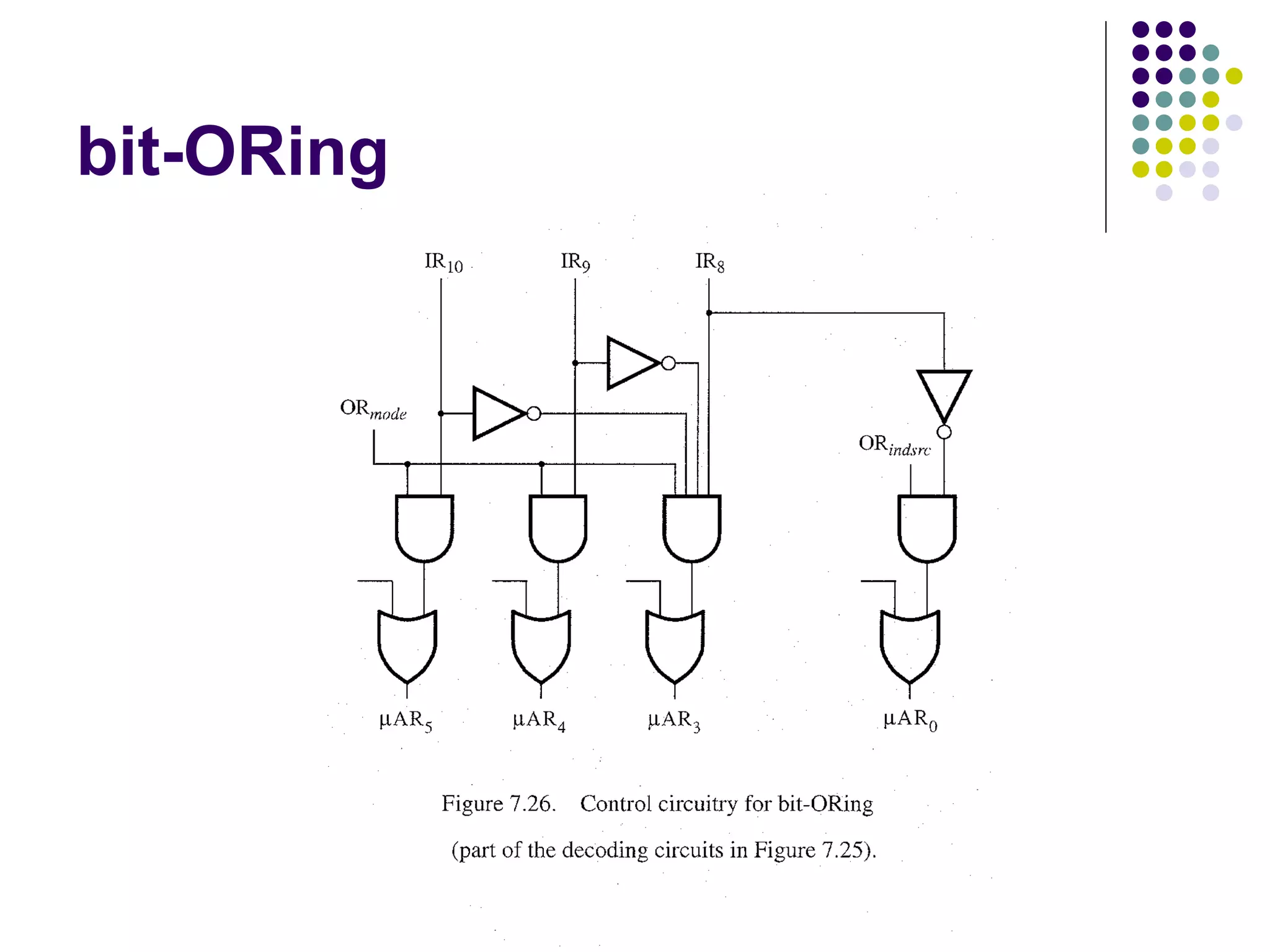
![OP code 0 1 0 Rsrc Rdst Mode Contents of IR 0 3 4 7 8 10 11 Figure 7.21. Microinstruction for Add (Rsrc)+,Rdst. Note:Microinstruction at location 170 is not executed for this addressing mode. Address Microinstruction (octal) 000 PC out, MARin, Read, Select 4, Add, Zin 001 Zout, PC in, Yin, WMFC 002 MDRout, IRin 003 Branch { PC 101 (from Instruction decoder); PC 5,4 [IR10,9 ]; PC 3 121 Rsrc out, MARin, Read, Select4, Add, Z in 122 Zout, Rsrc in 123 170 MDRout, MARin, Read, WMFC 171 MDRout, Yin 172 Rdst out, SelectY , Add, Zin 173 Zout, Rdst in, End [IR10] [IR9] [IR8]} Branch { PC 170;PC 0 [IR8]}, WMFC](https://image.slidesharecdn.com/chapter3-basicprocessingunit-230401033245-413b61f8/75/chapter3-Basic-Processing-Unit-ppt-41-2048.jpg)