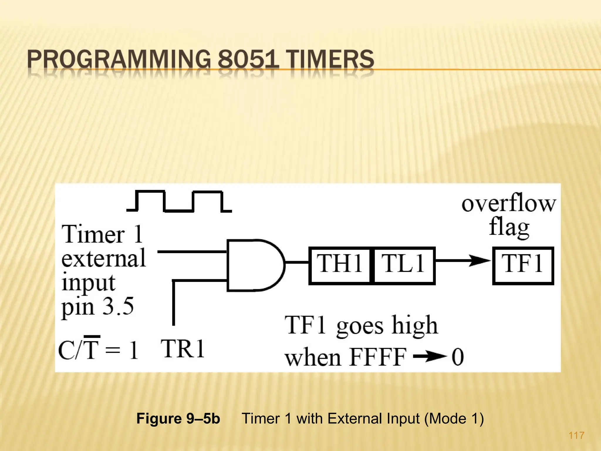
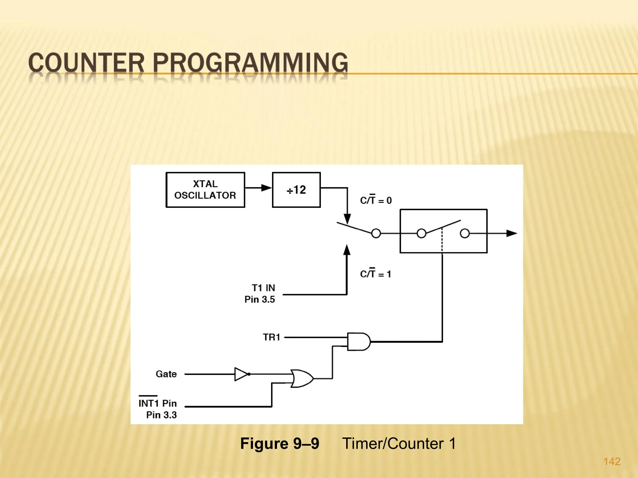
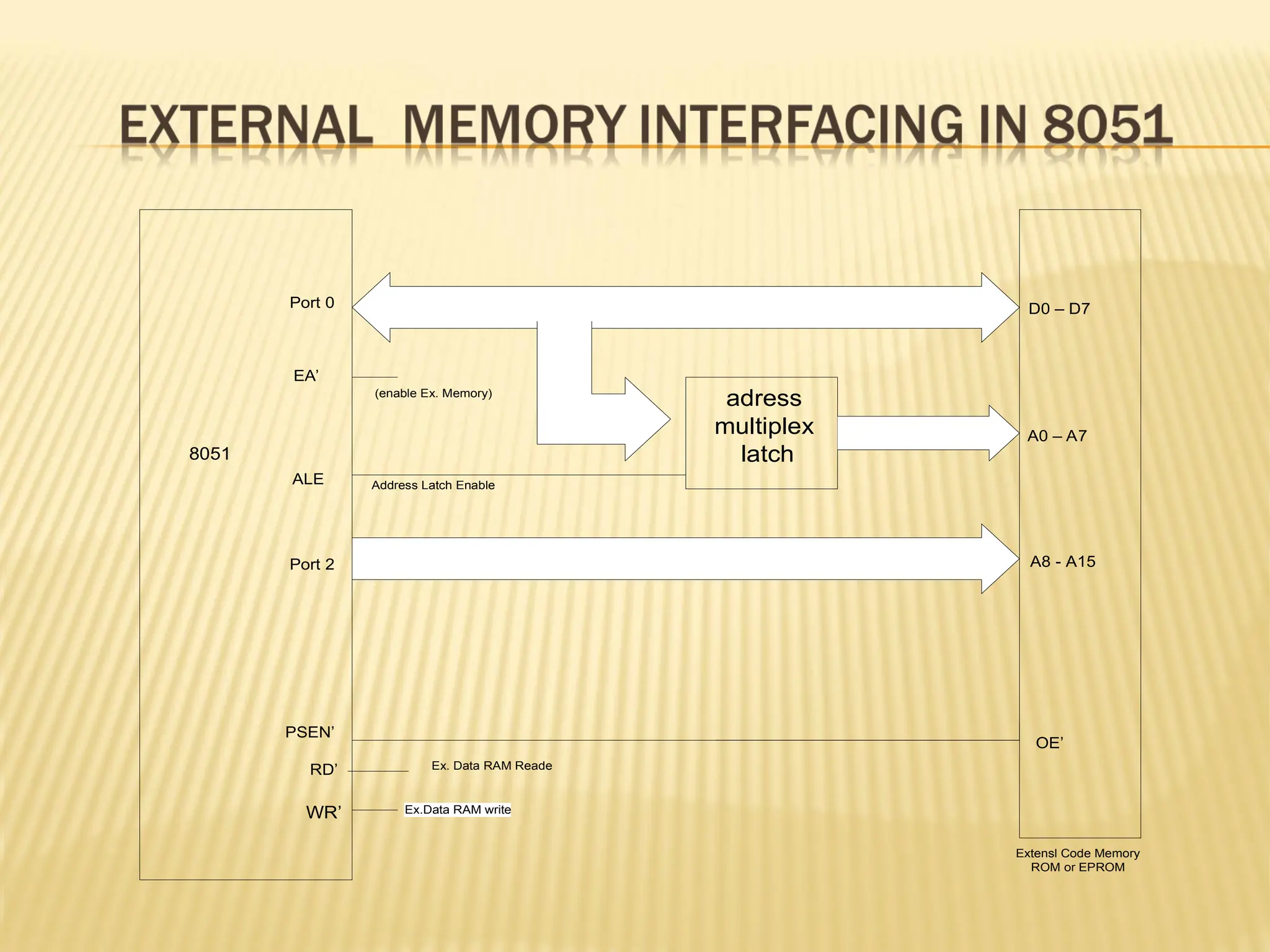
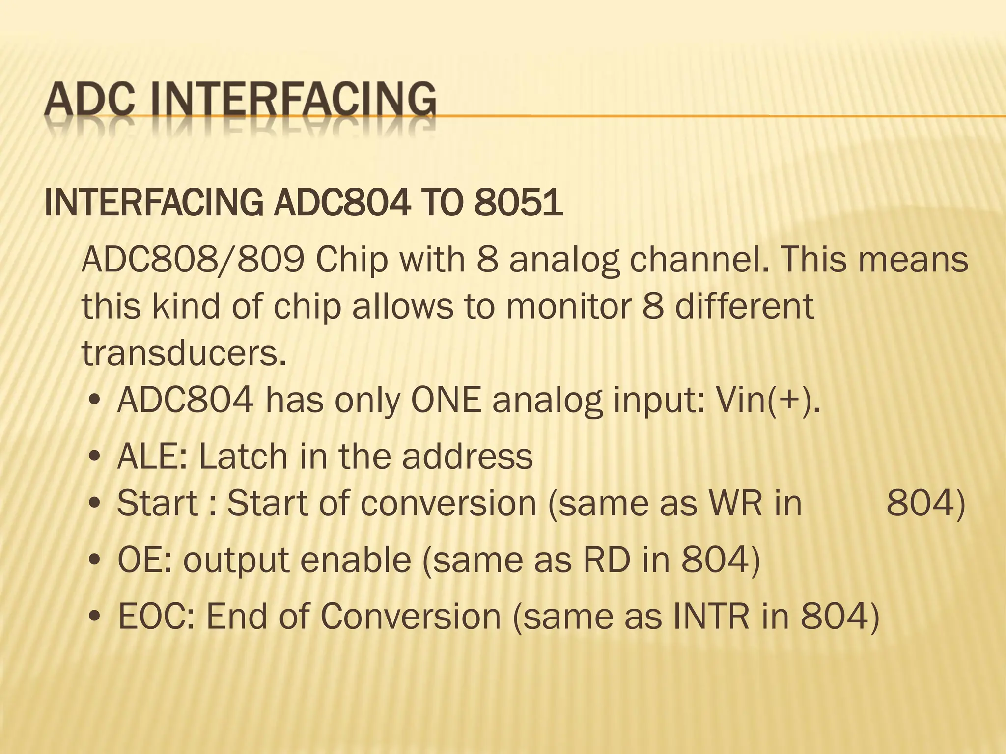
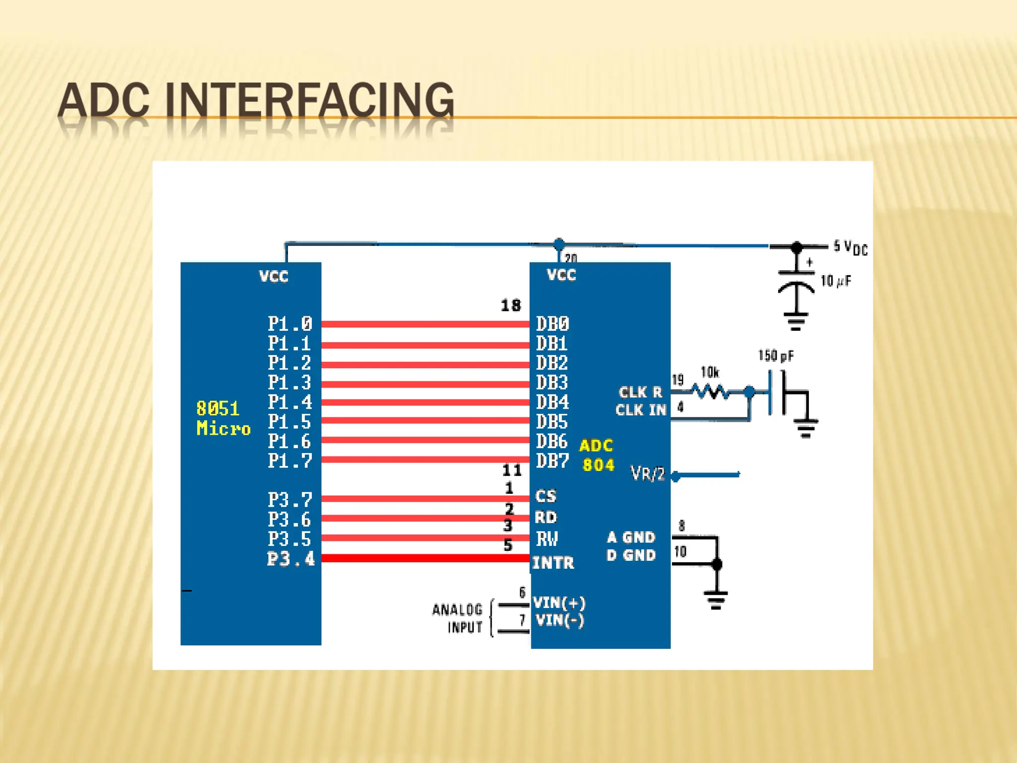
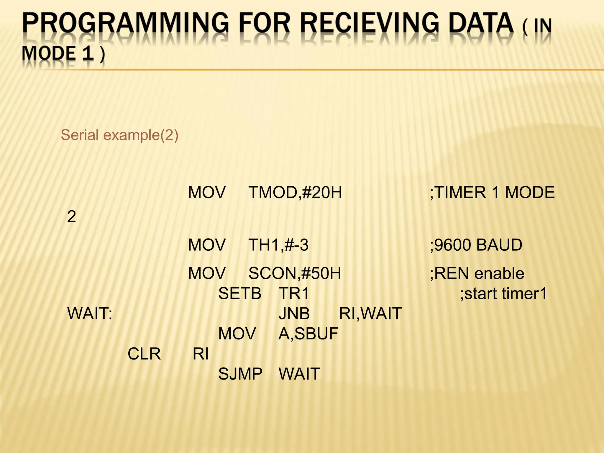
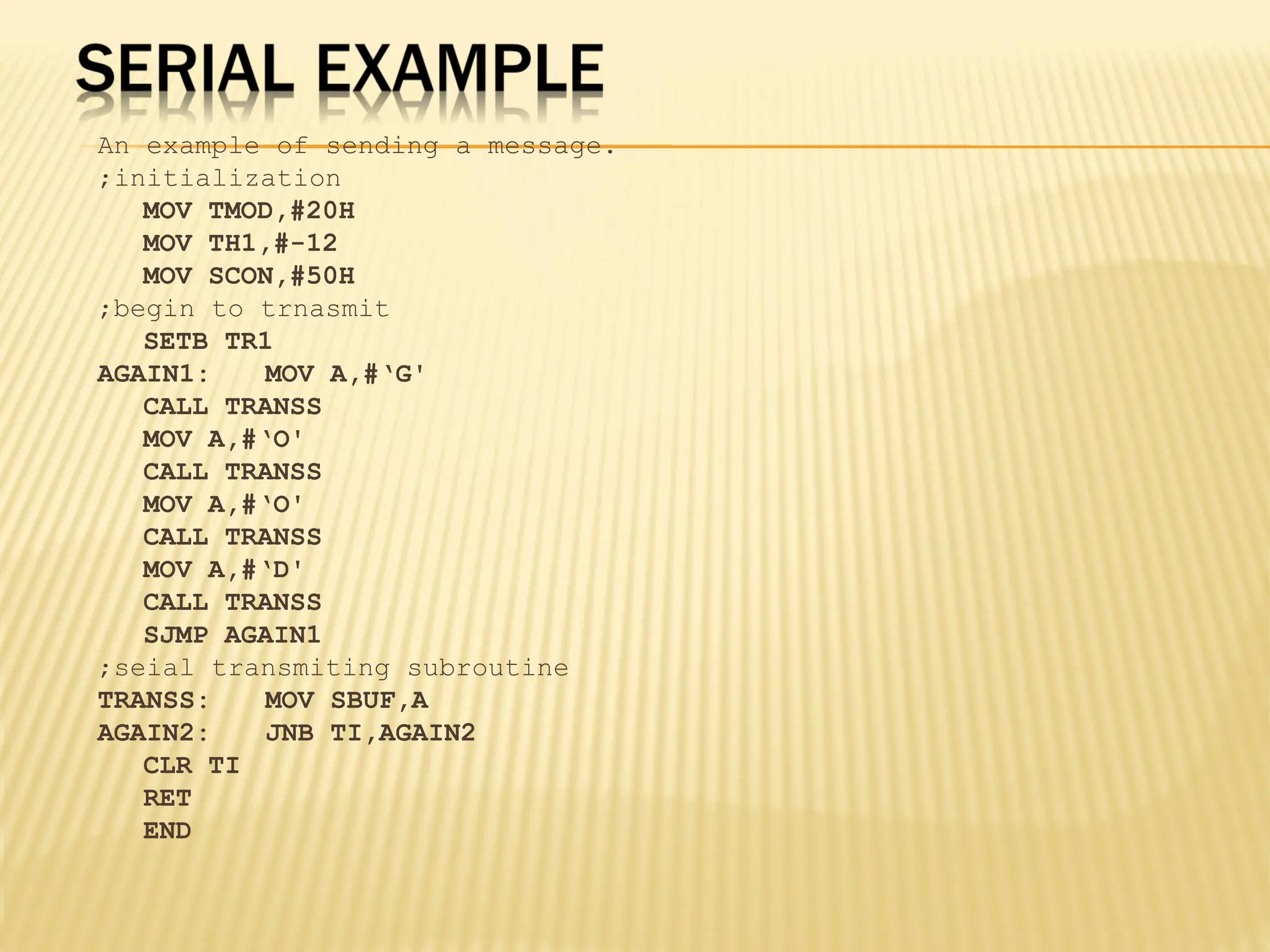
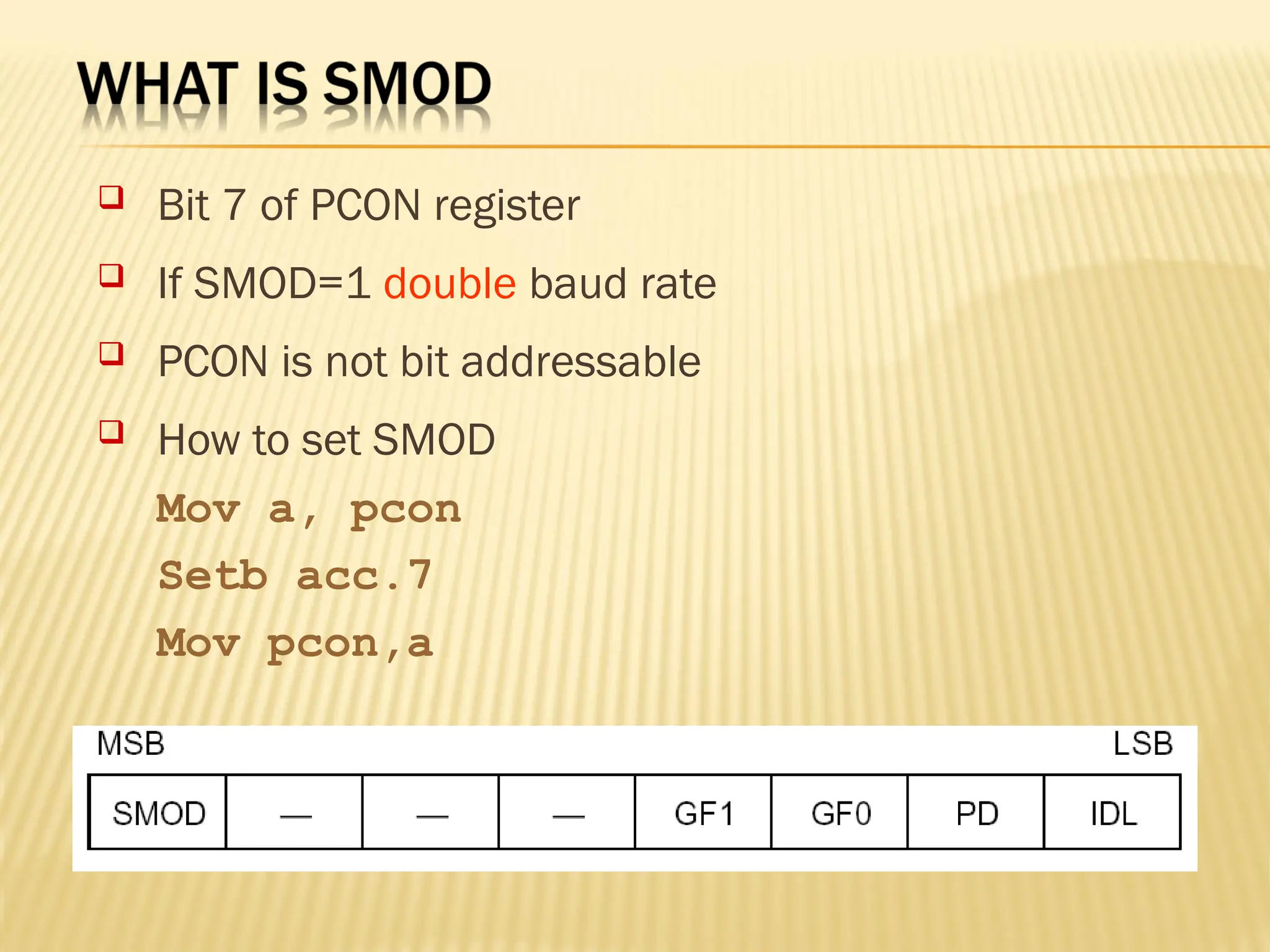
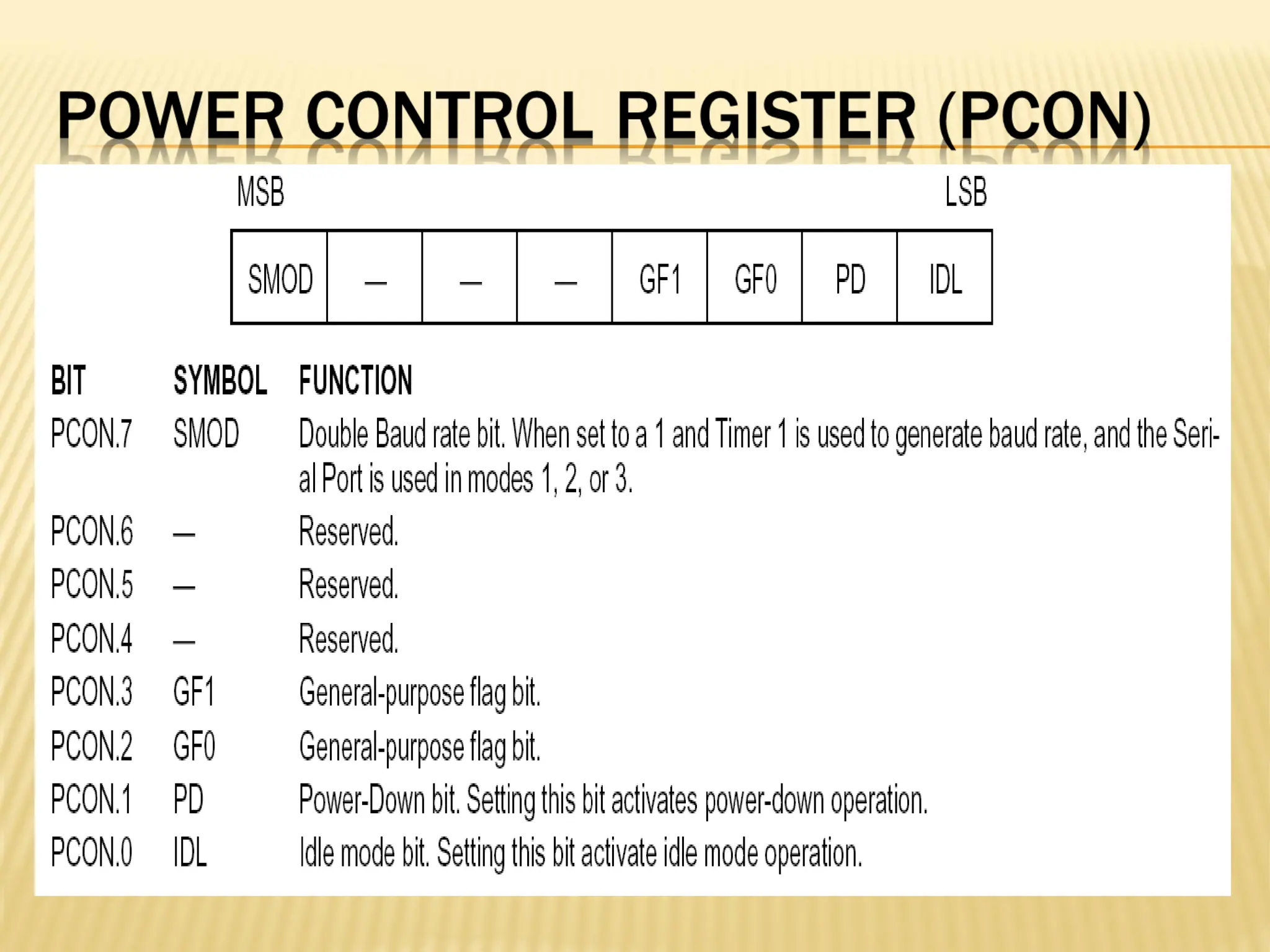
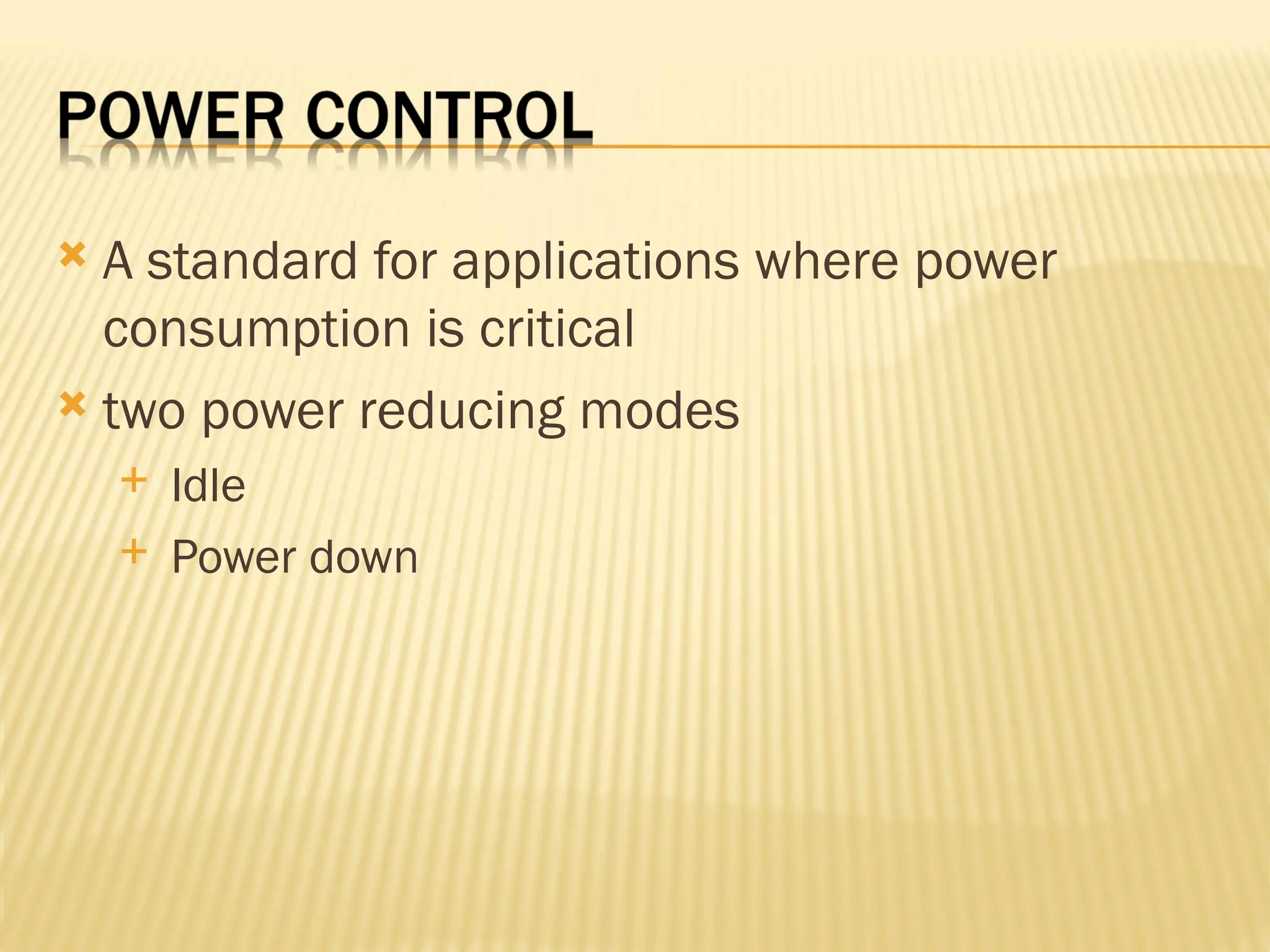
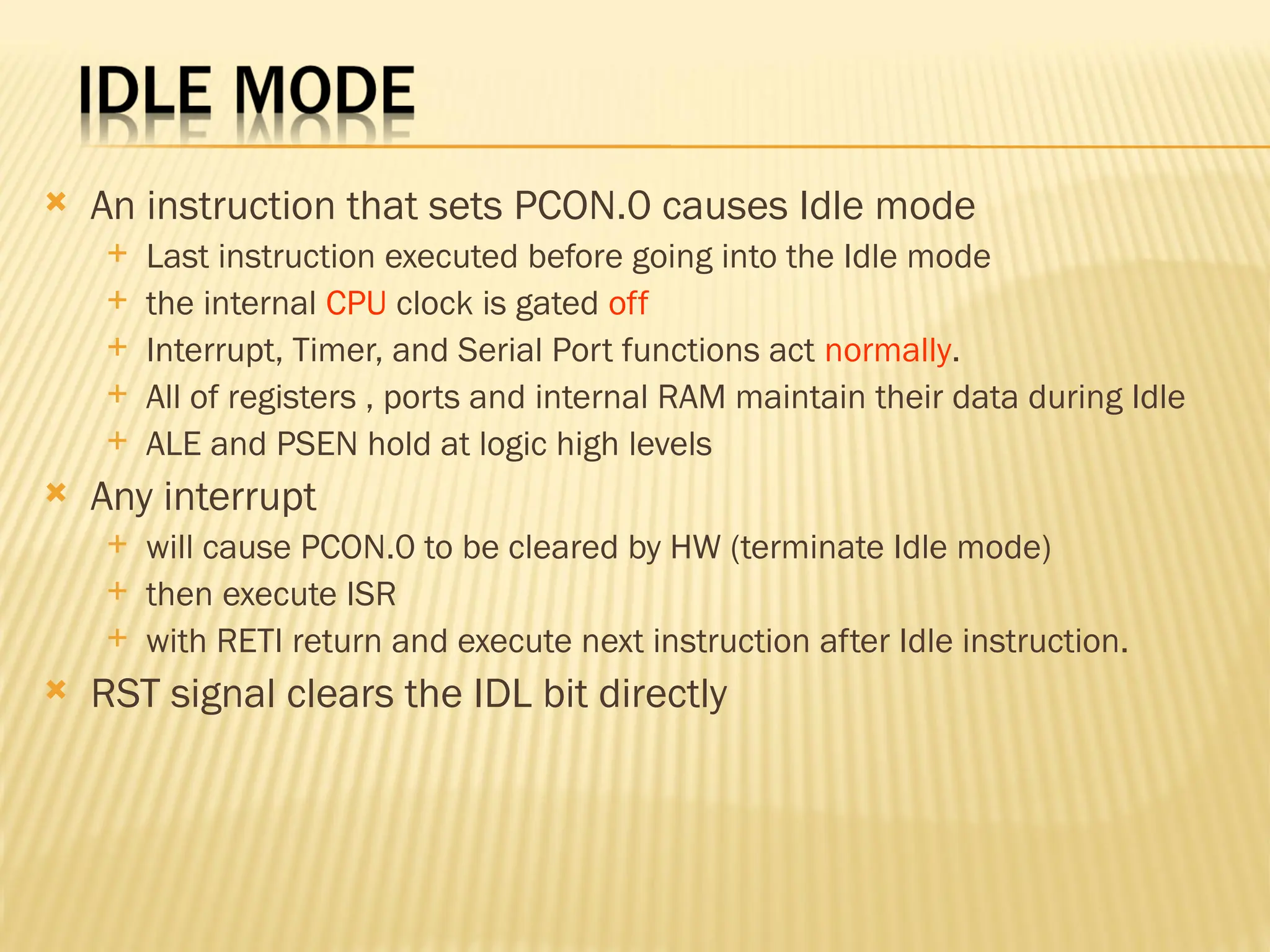
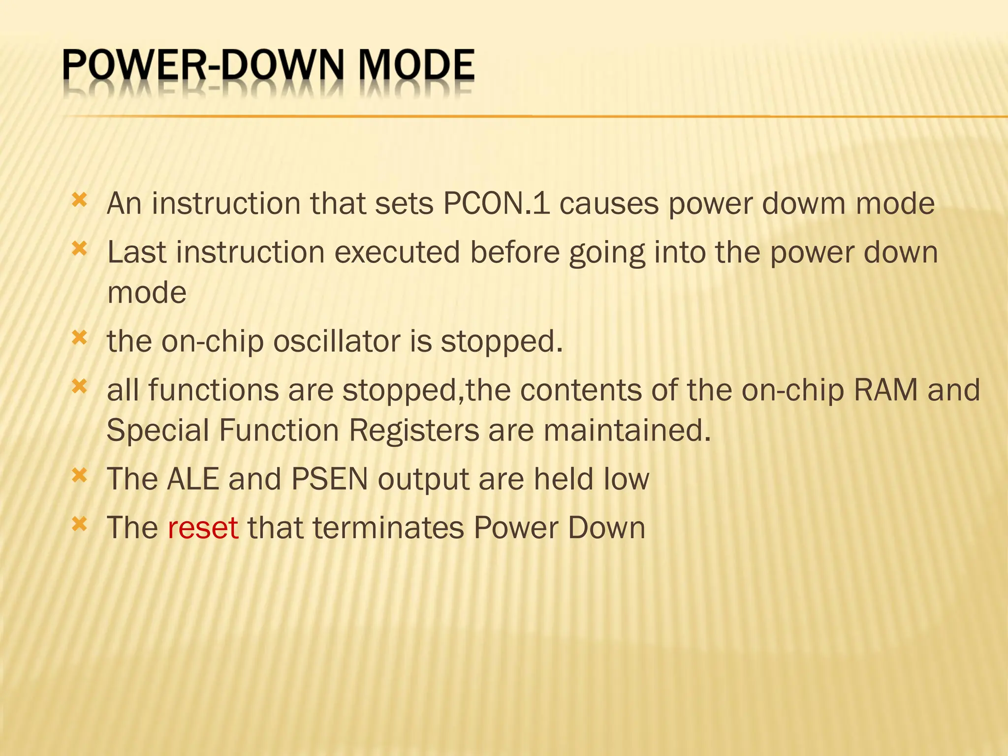
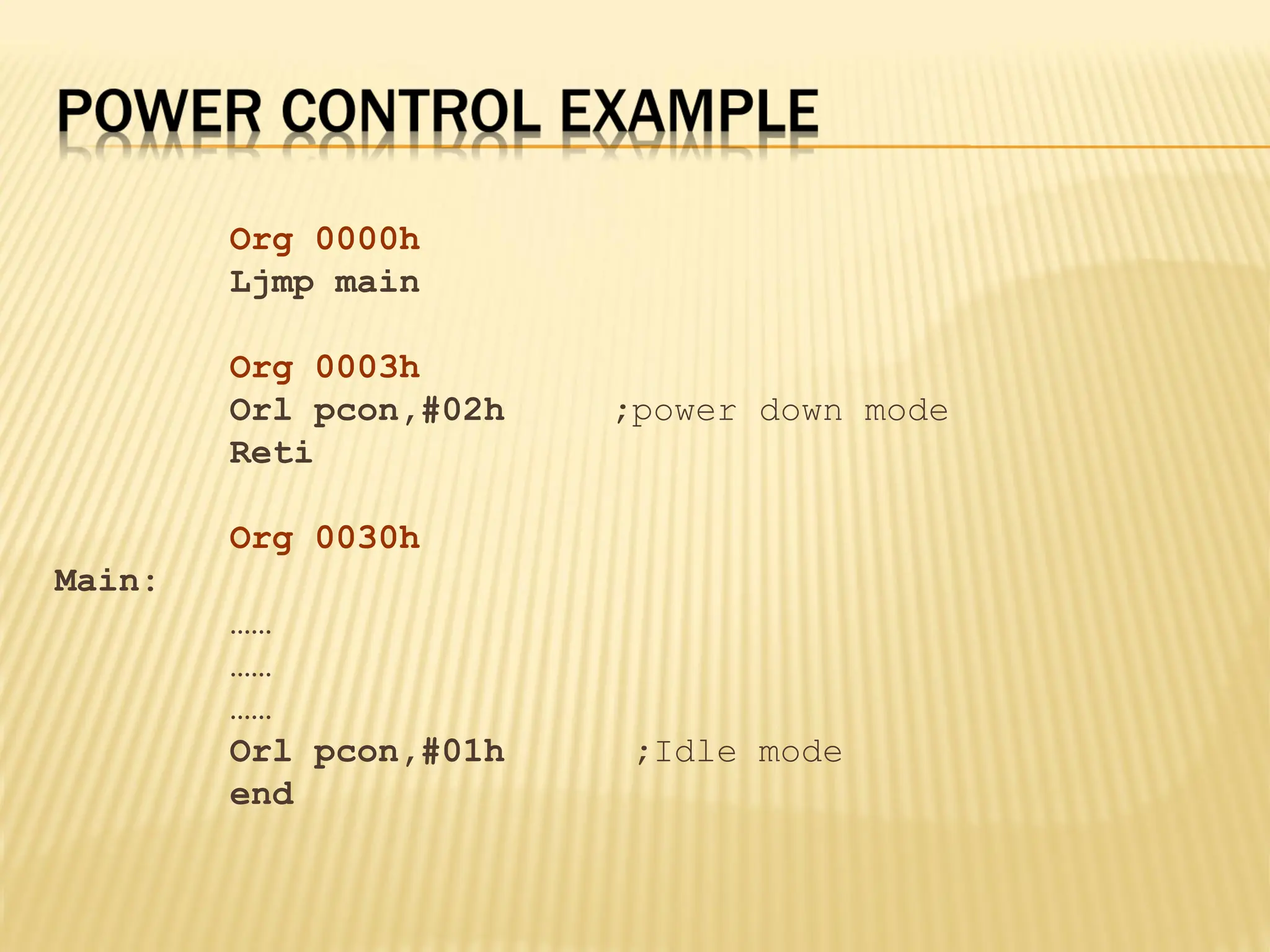
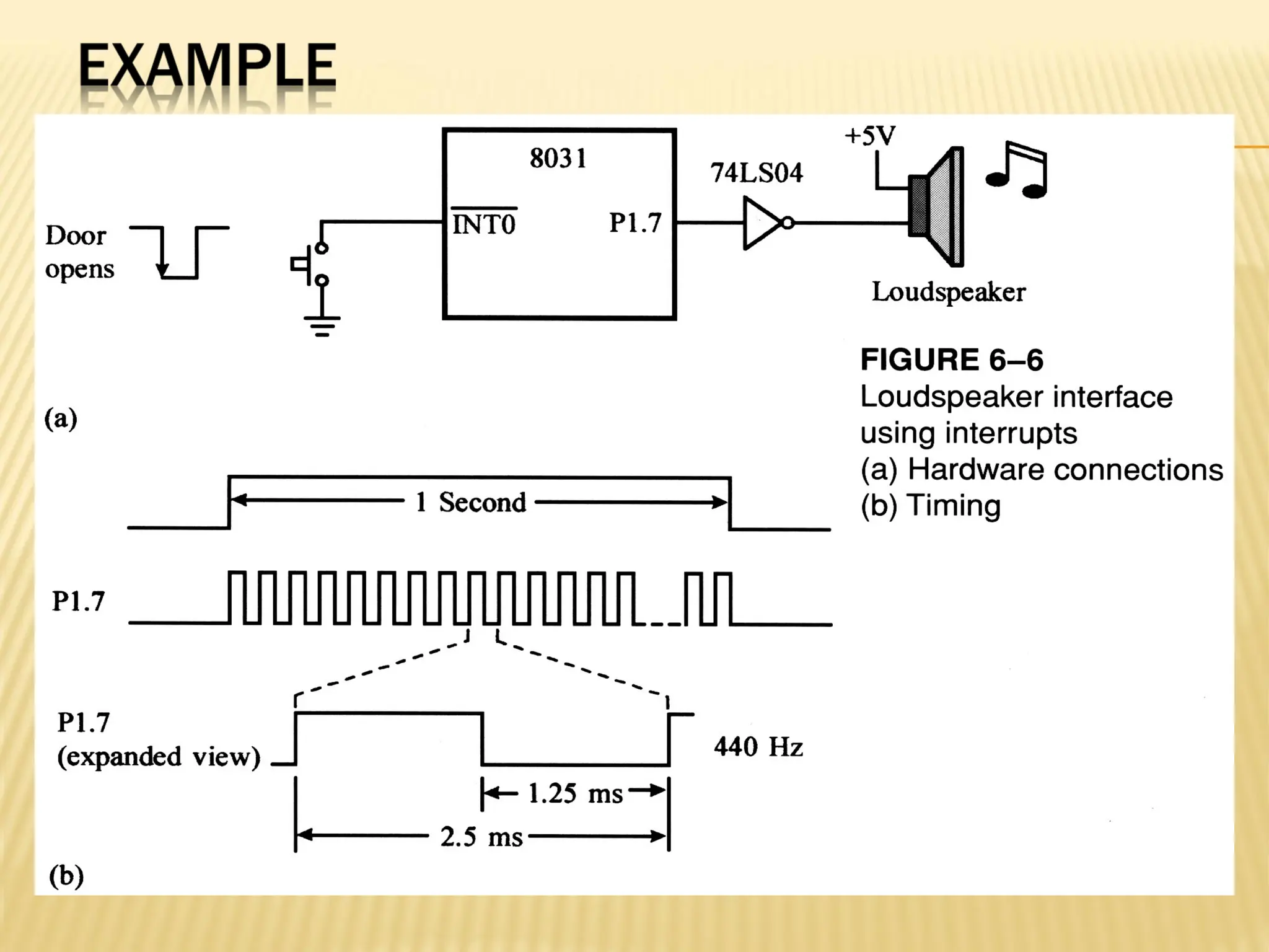
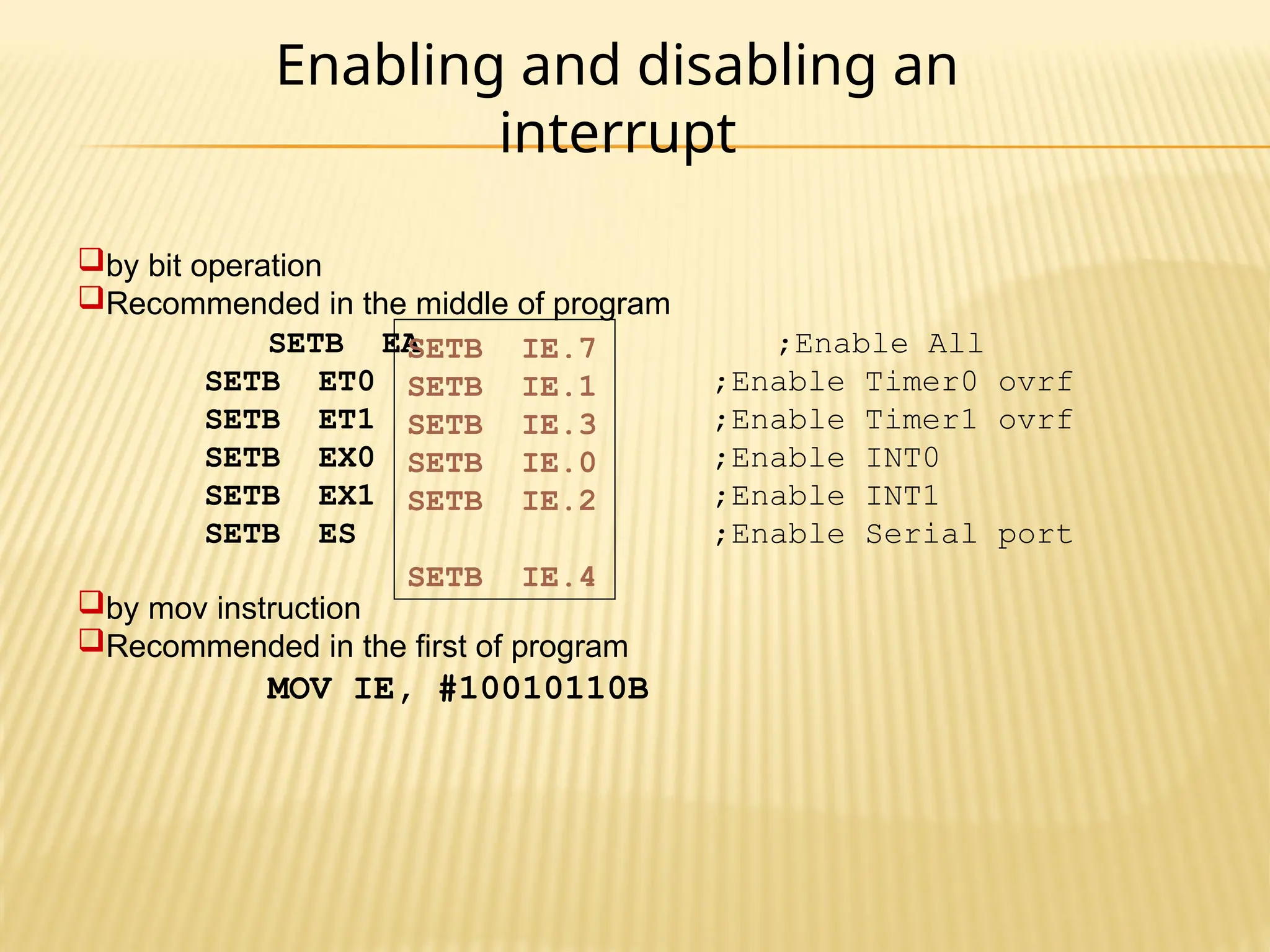
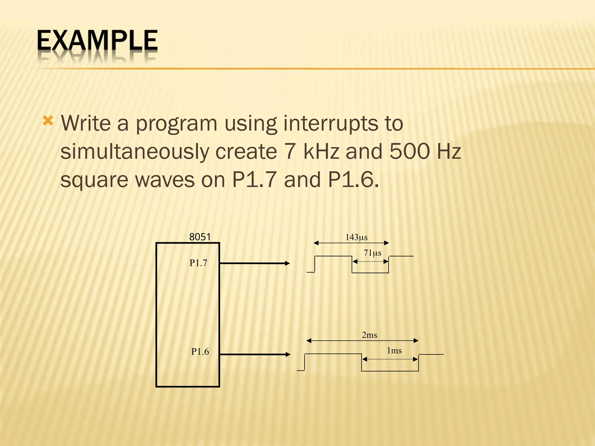
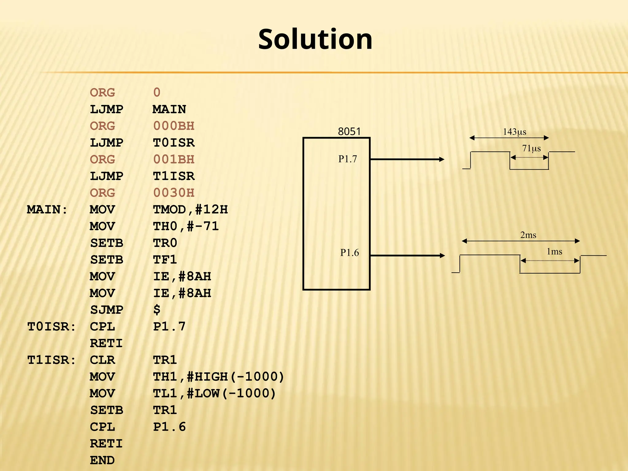
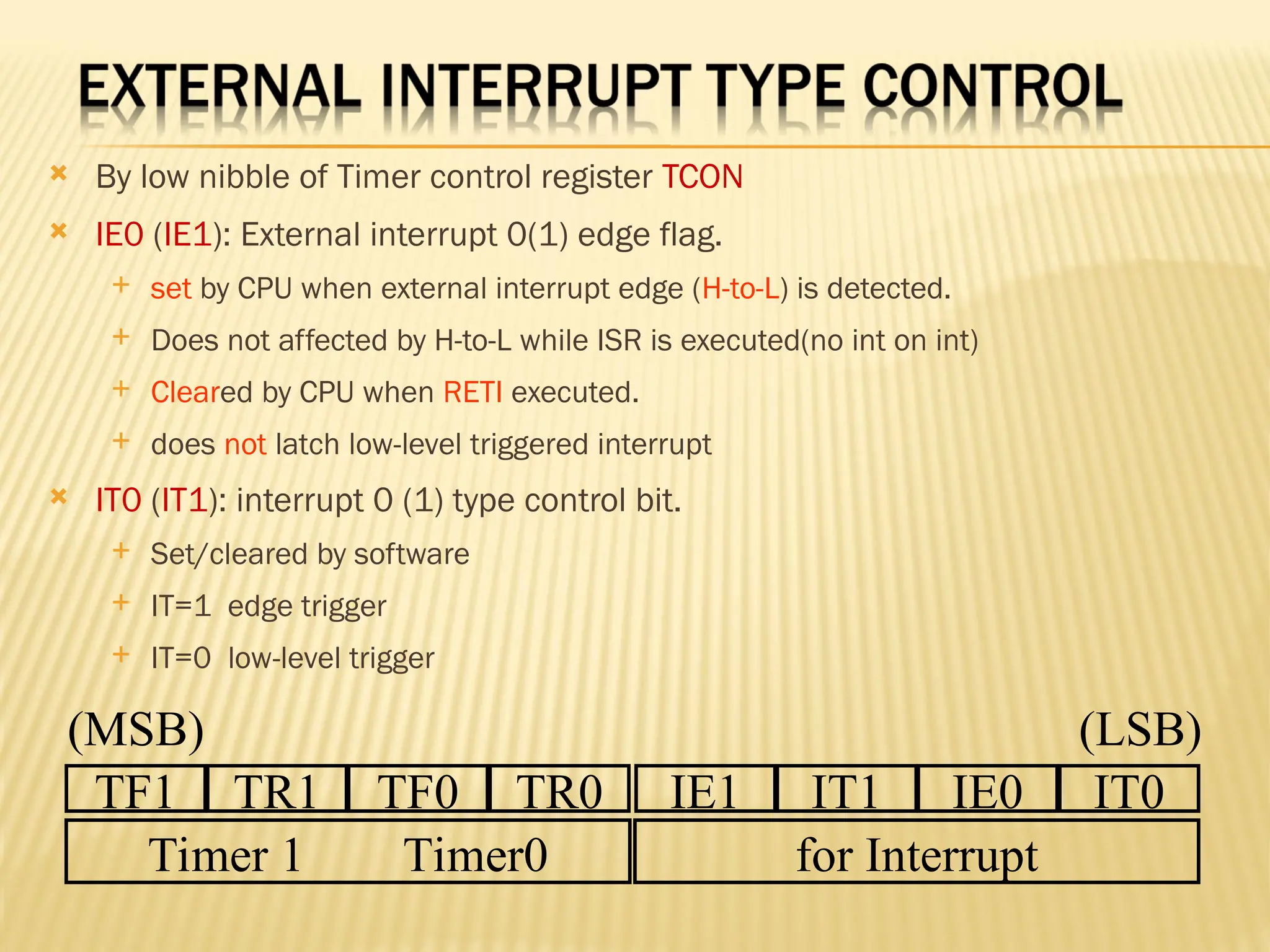
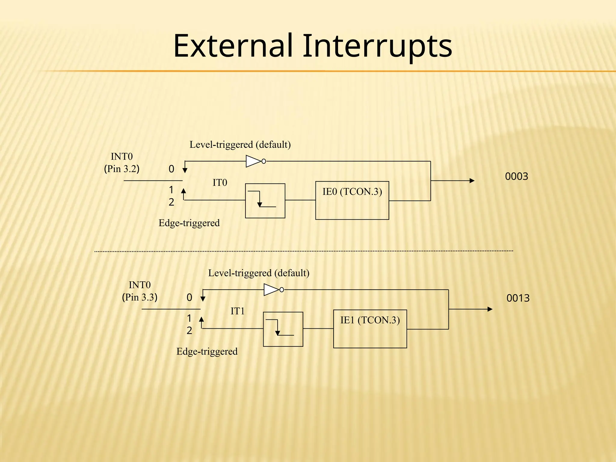
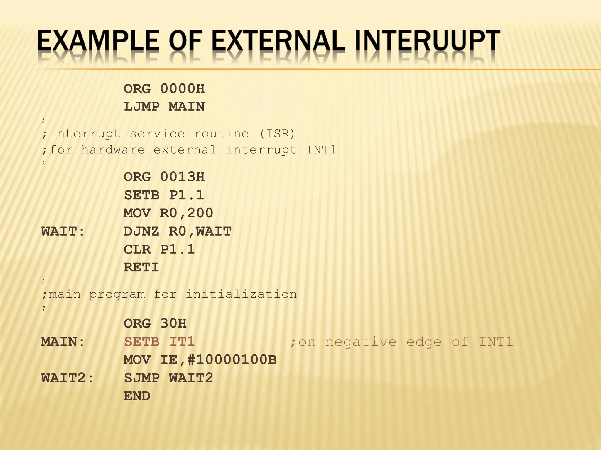
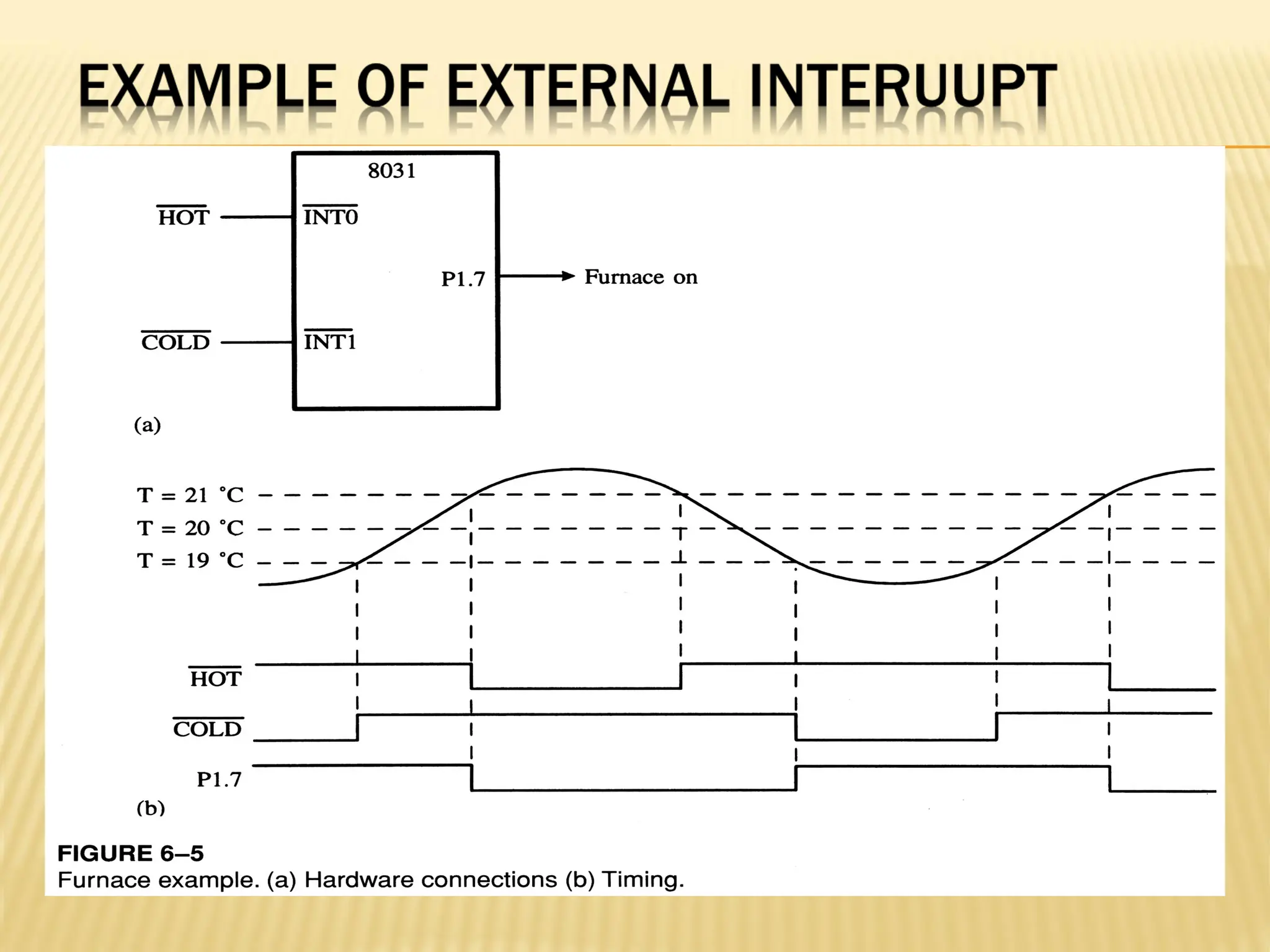
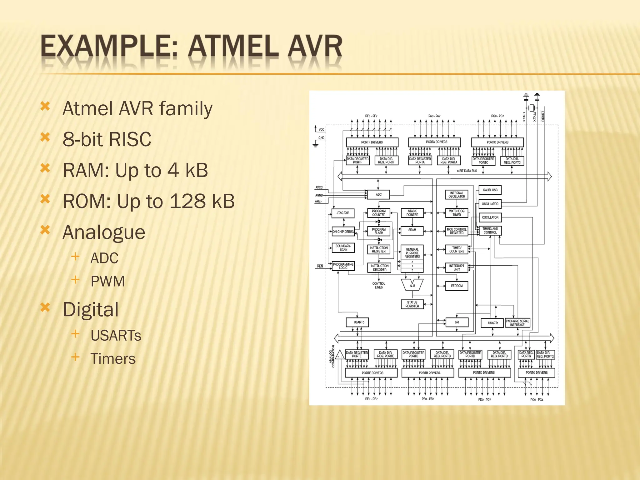
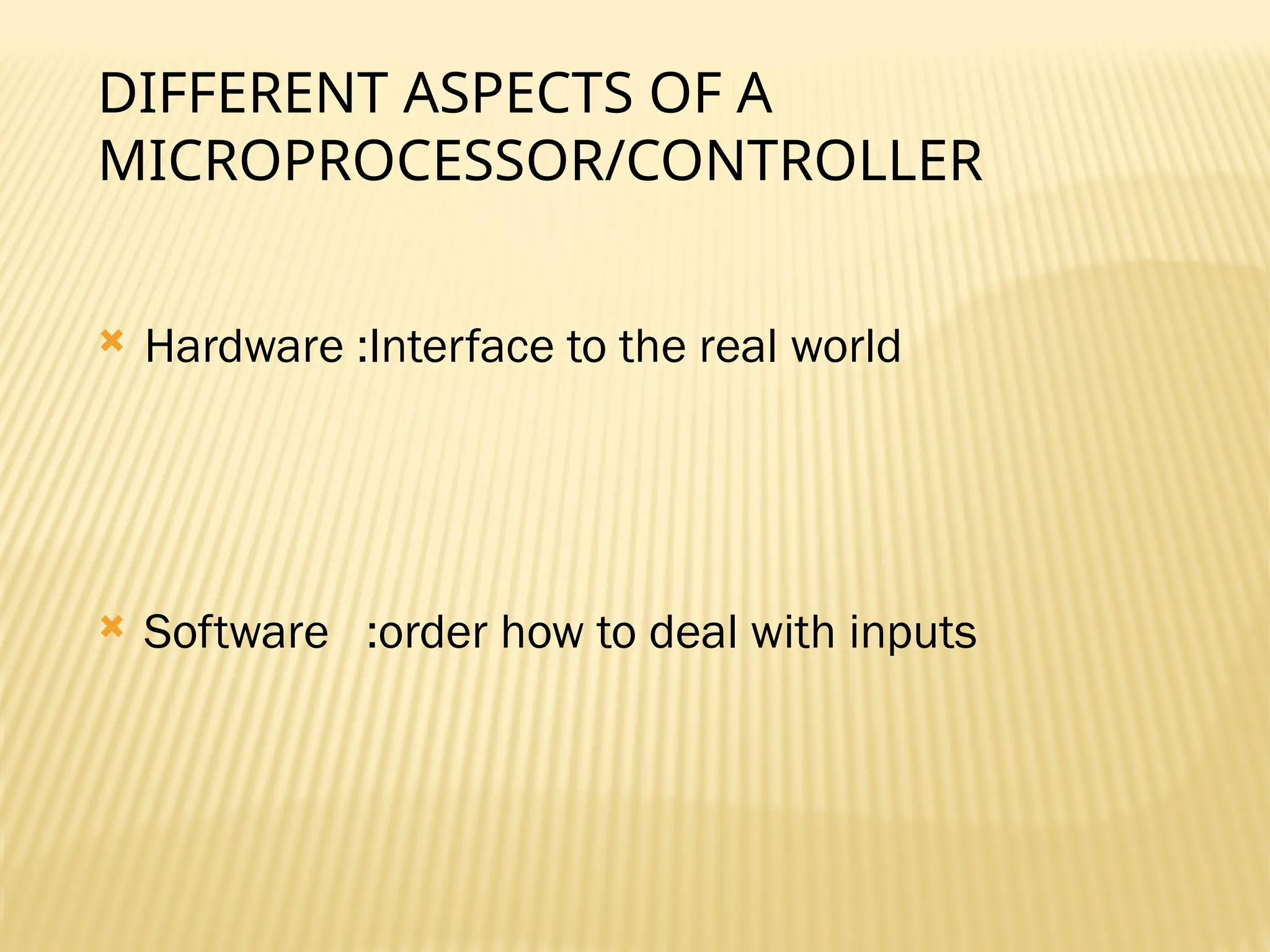
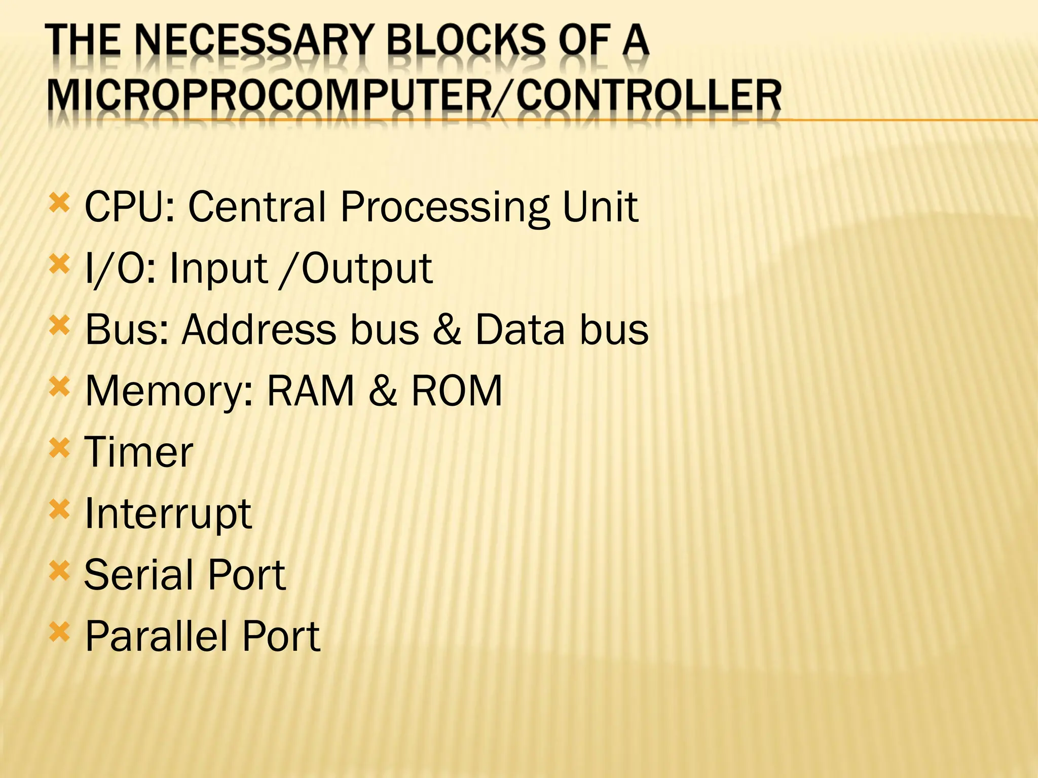
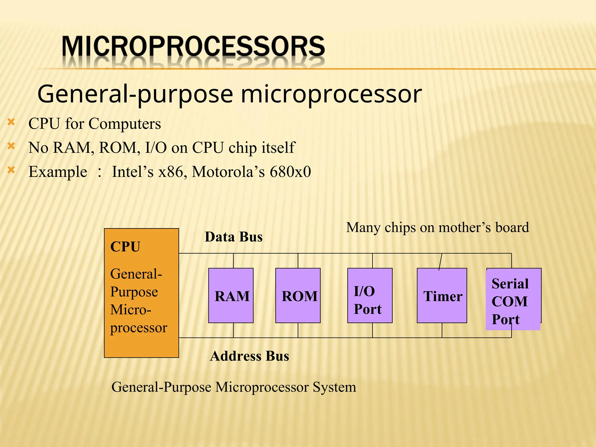
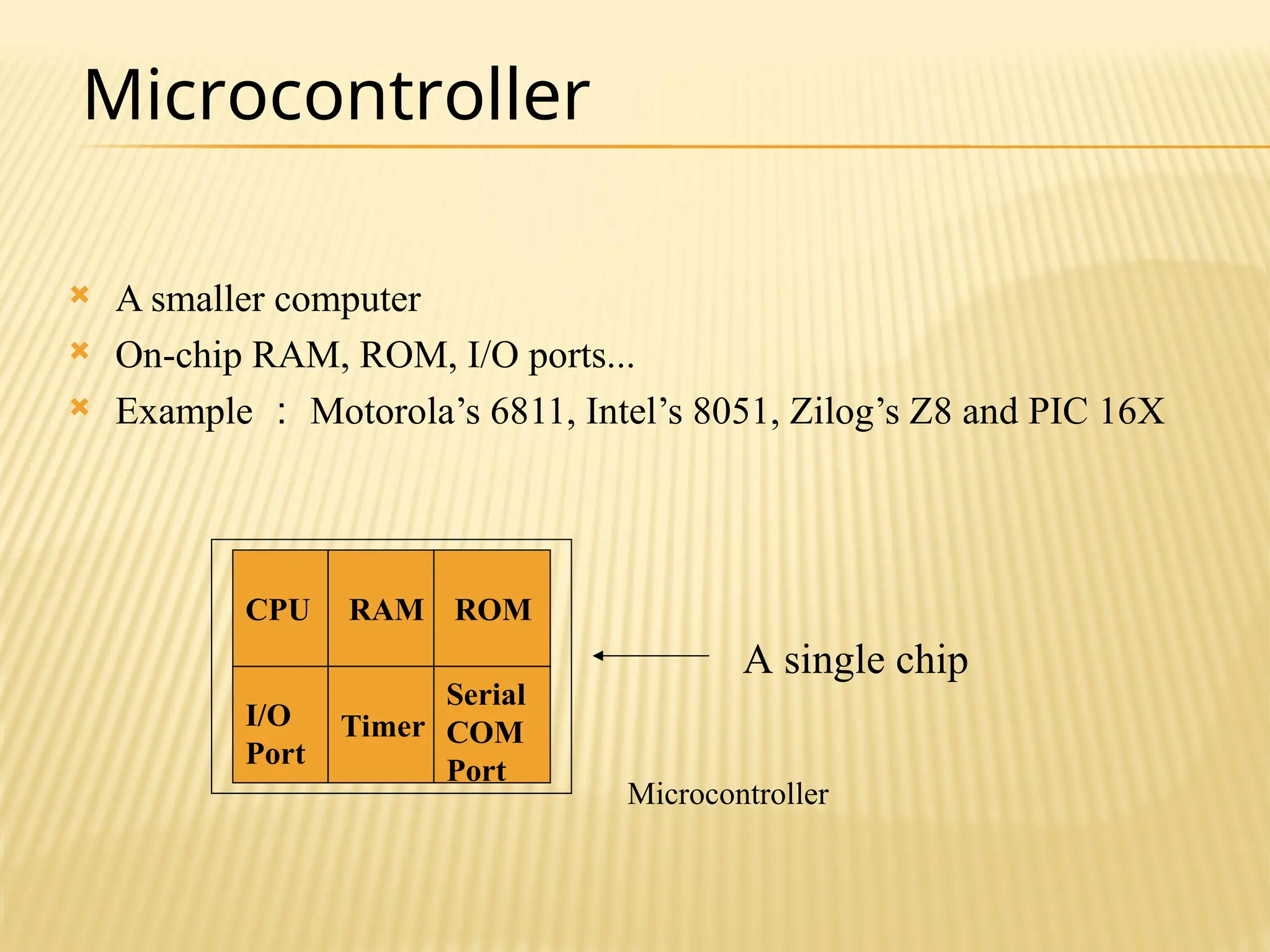
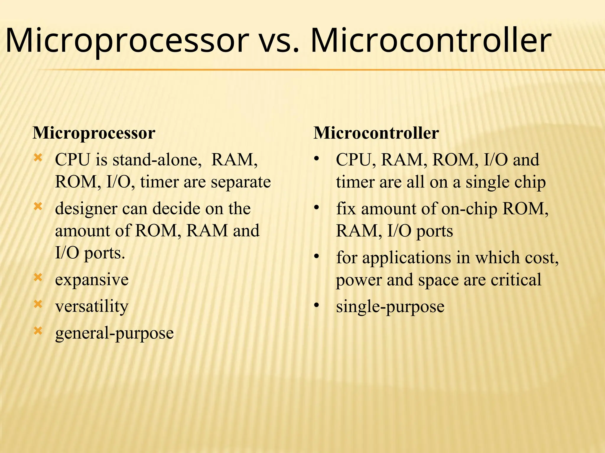
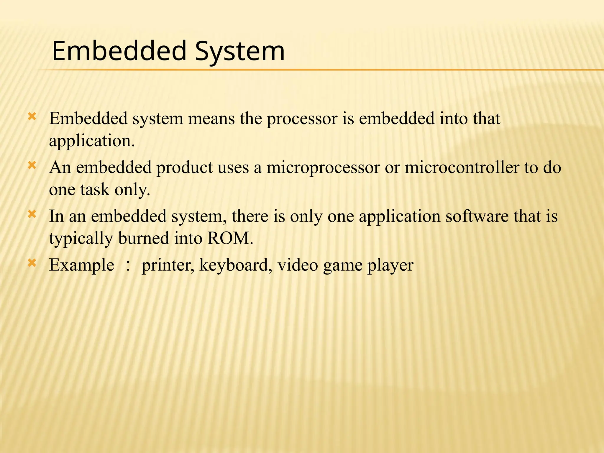
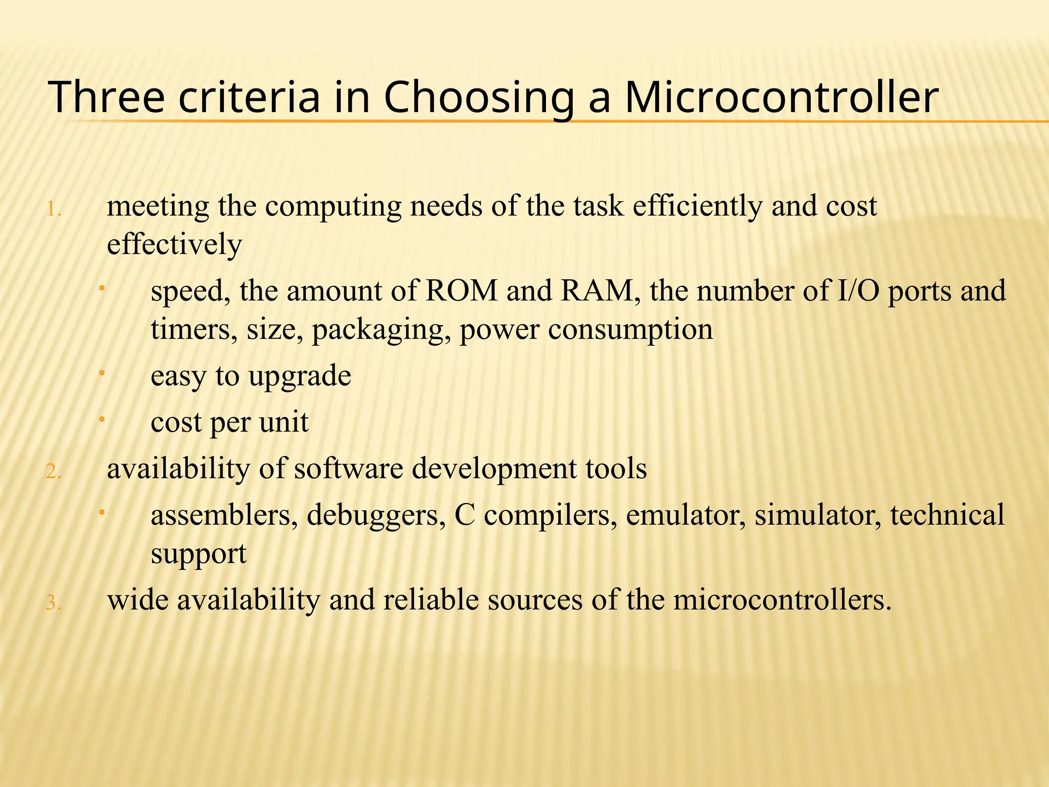
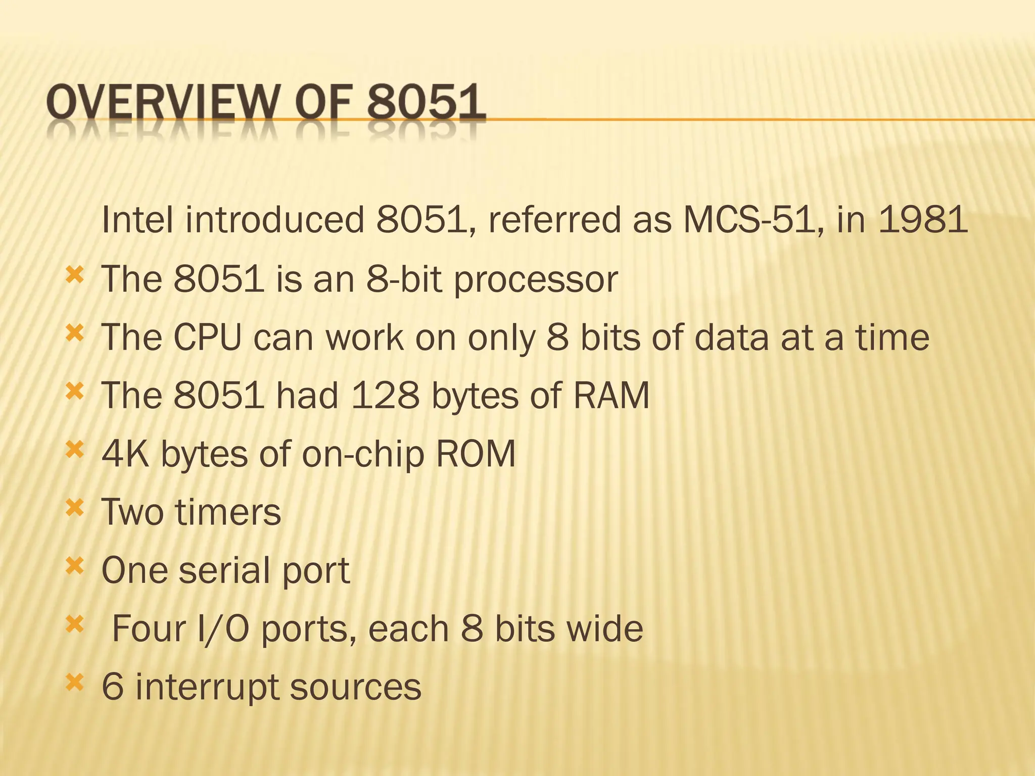
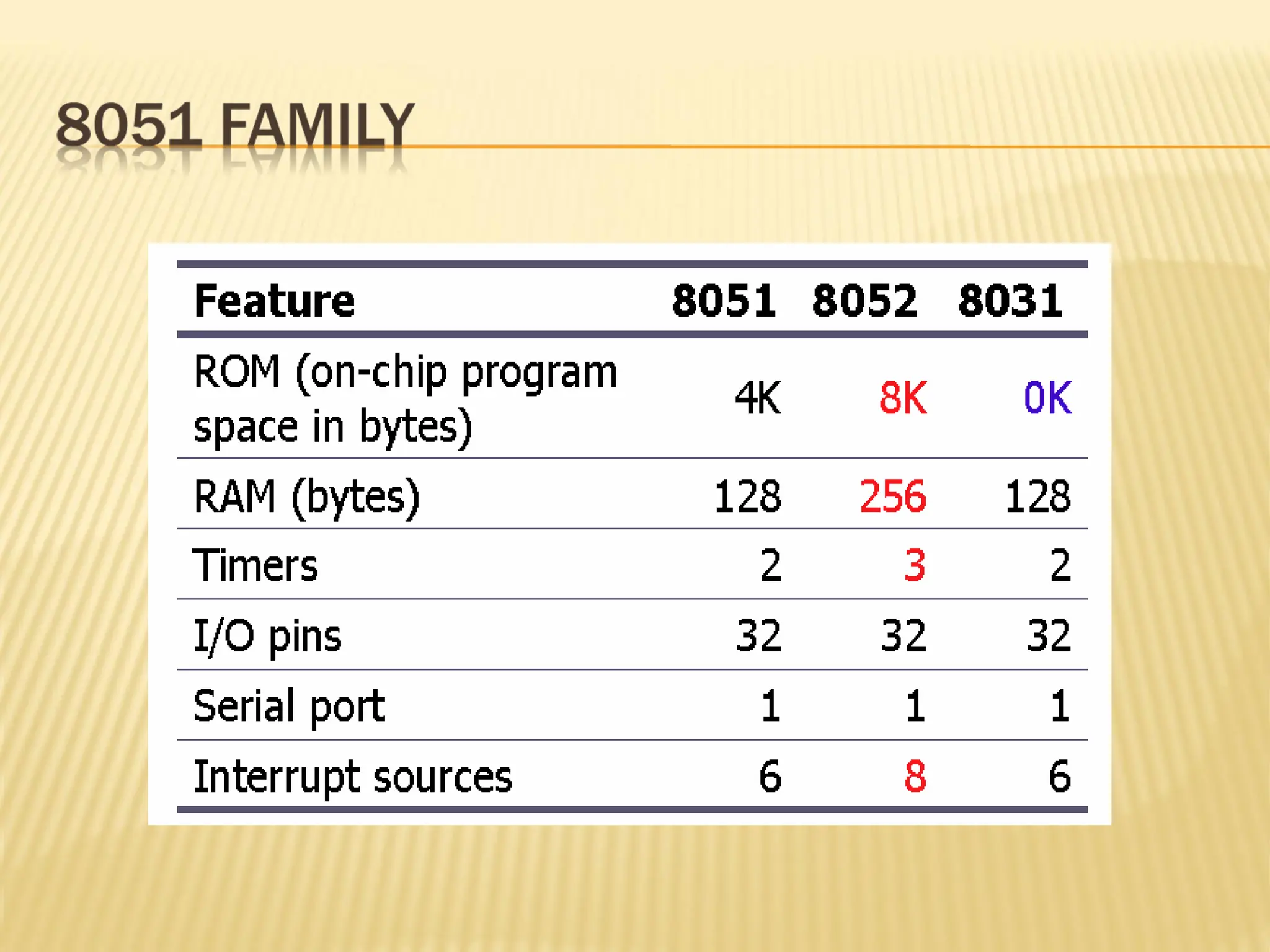
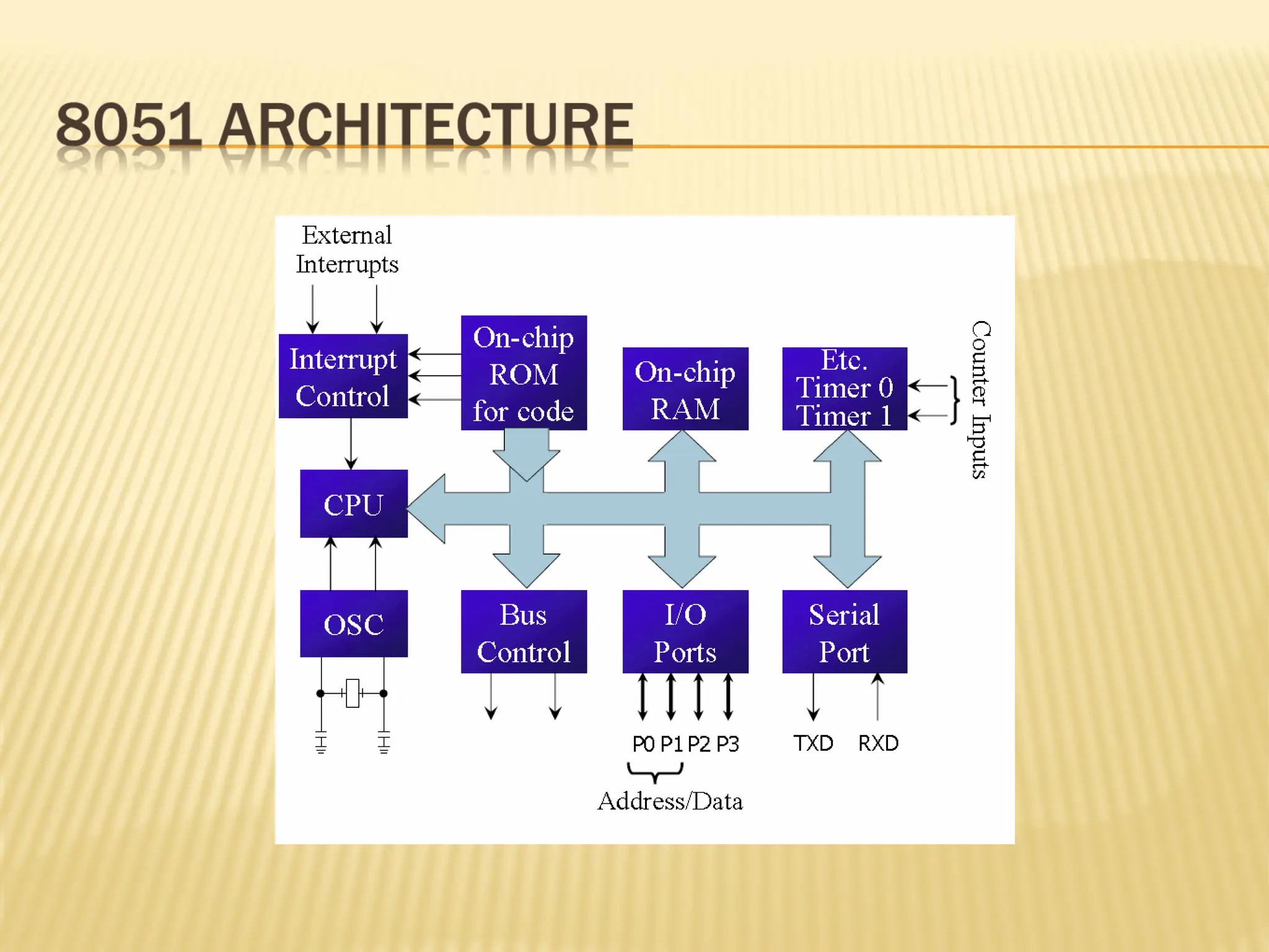
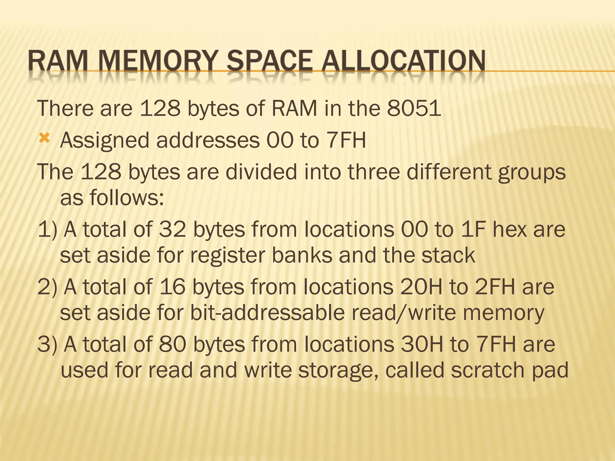
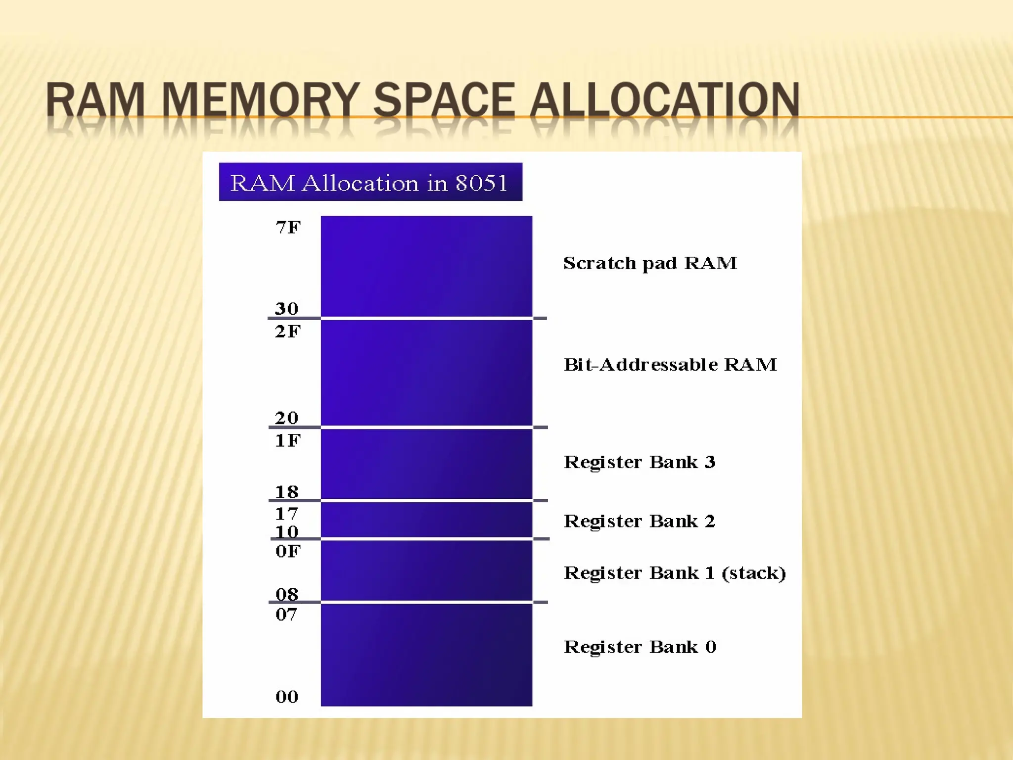
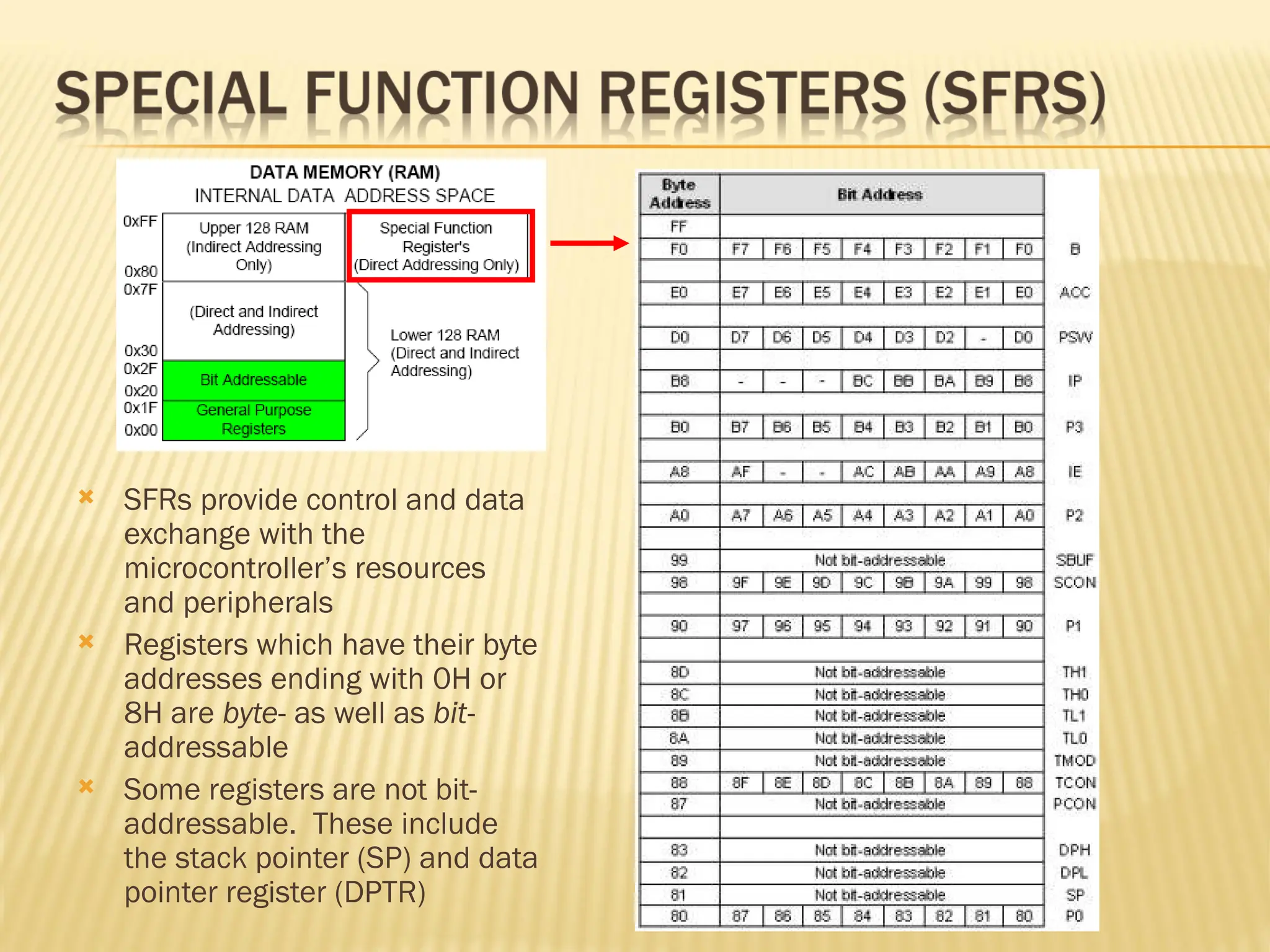
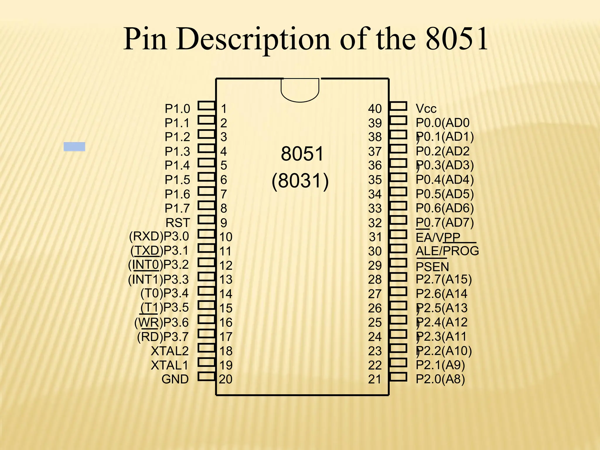
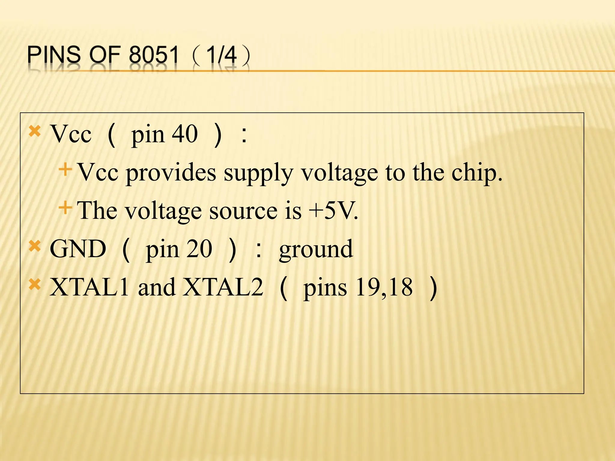
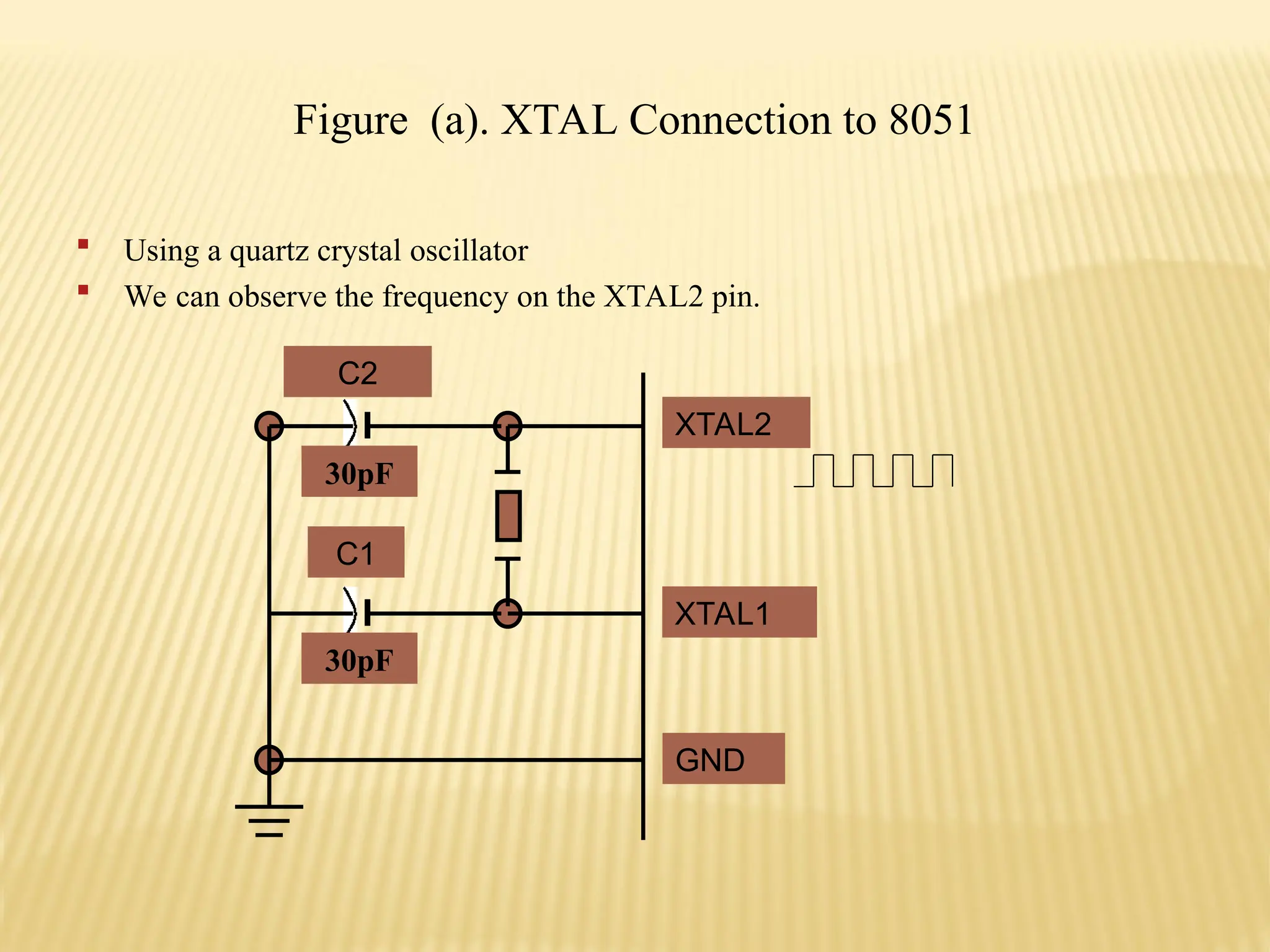
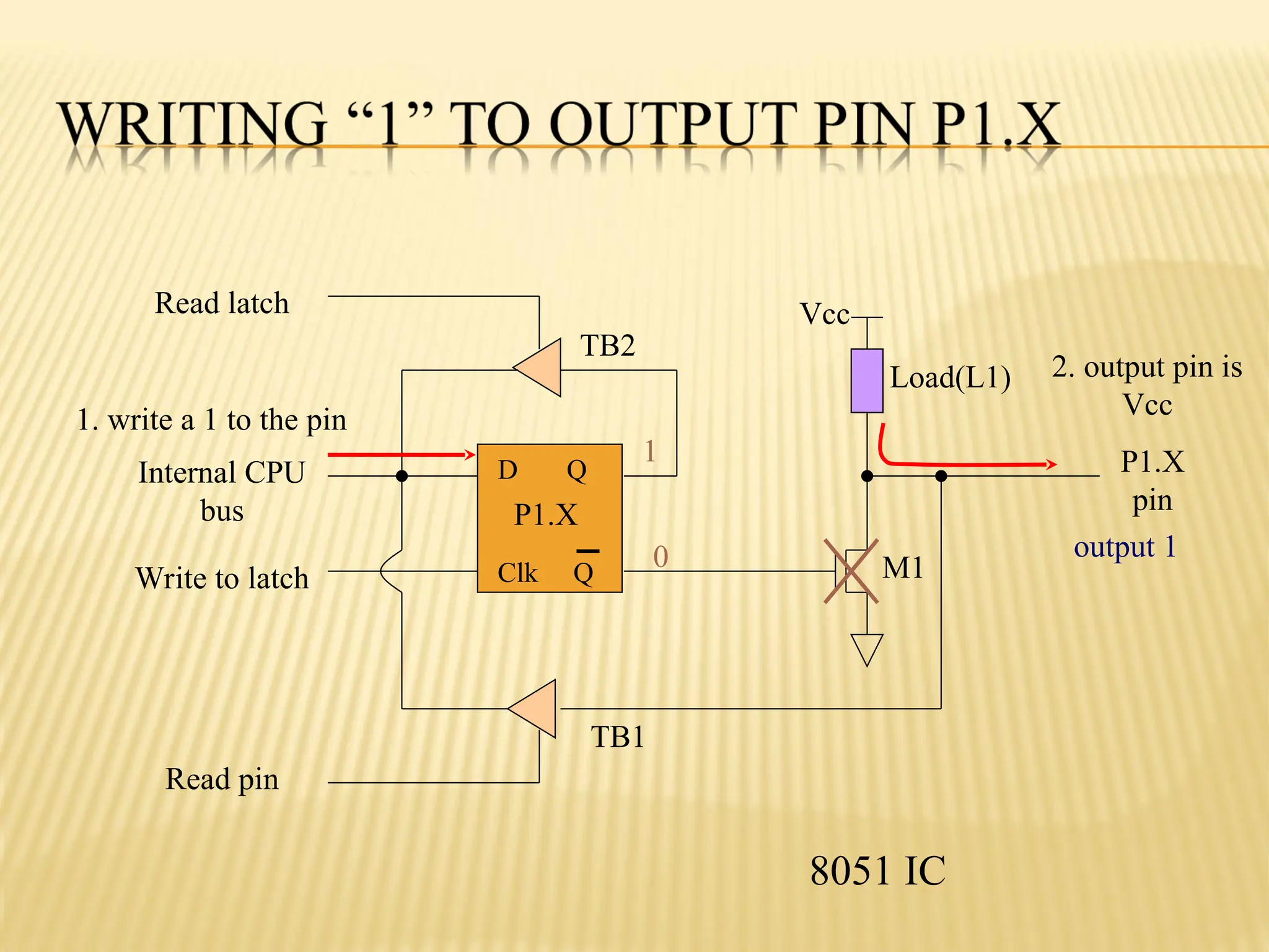
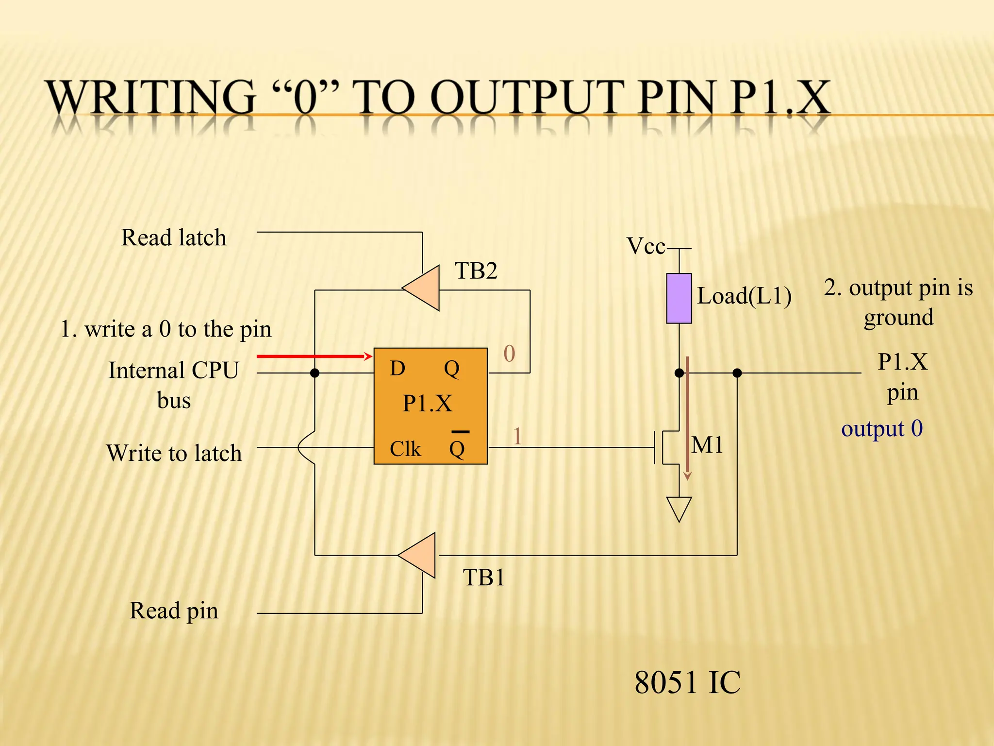
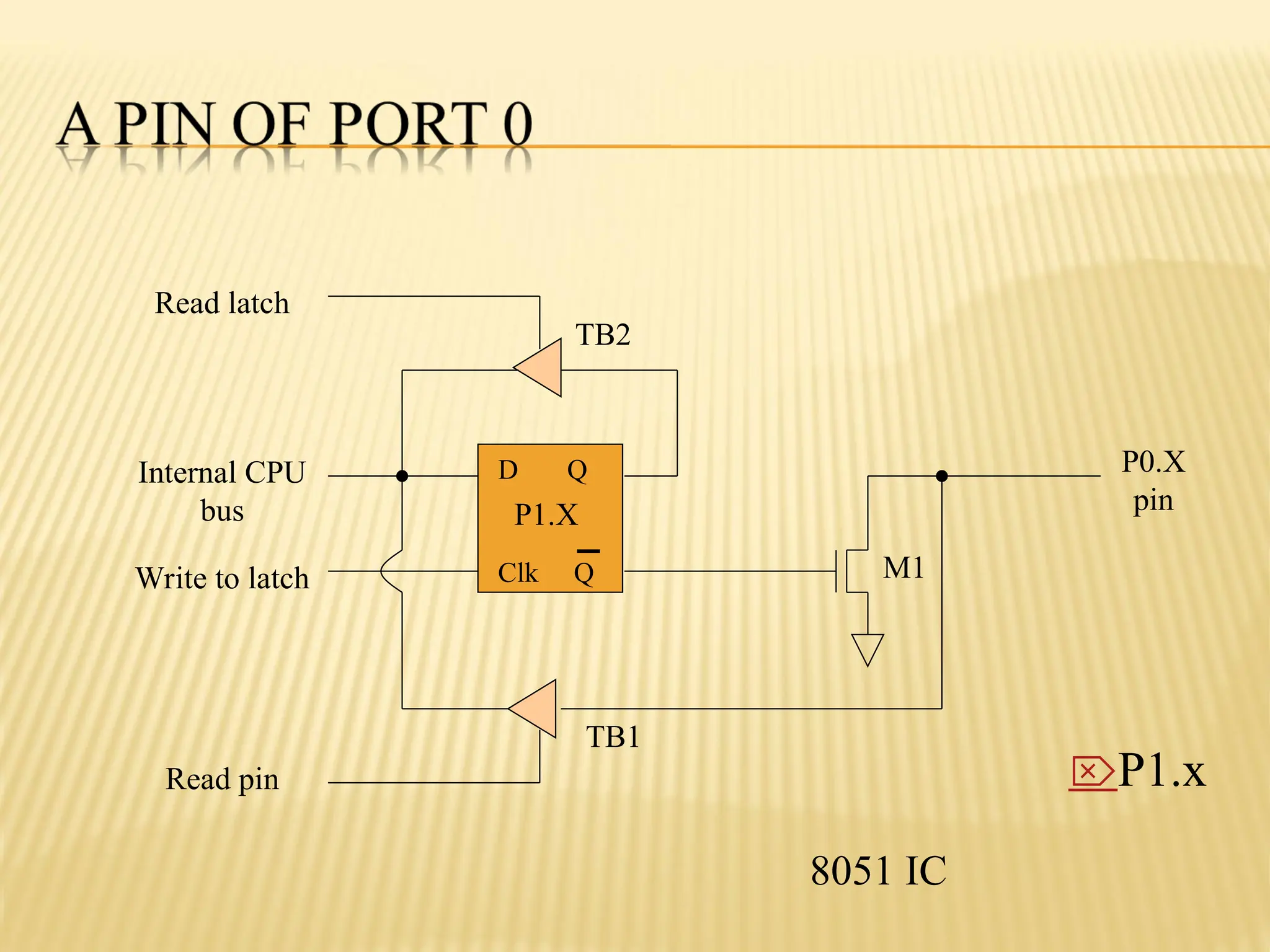
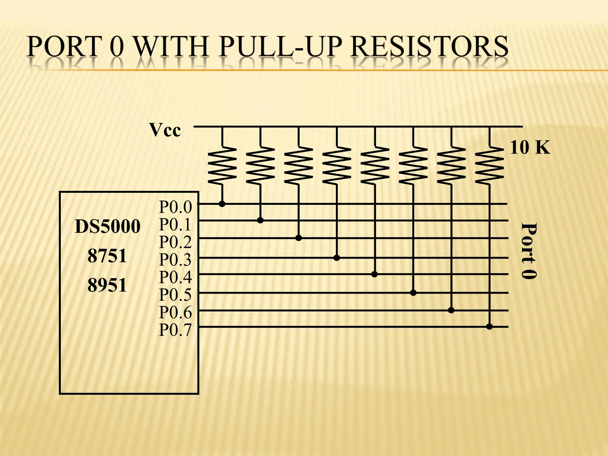
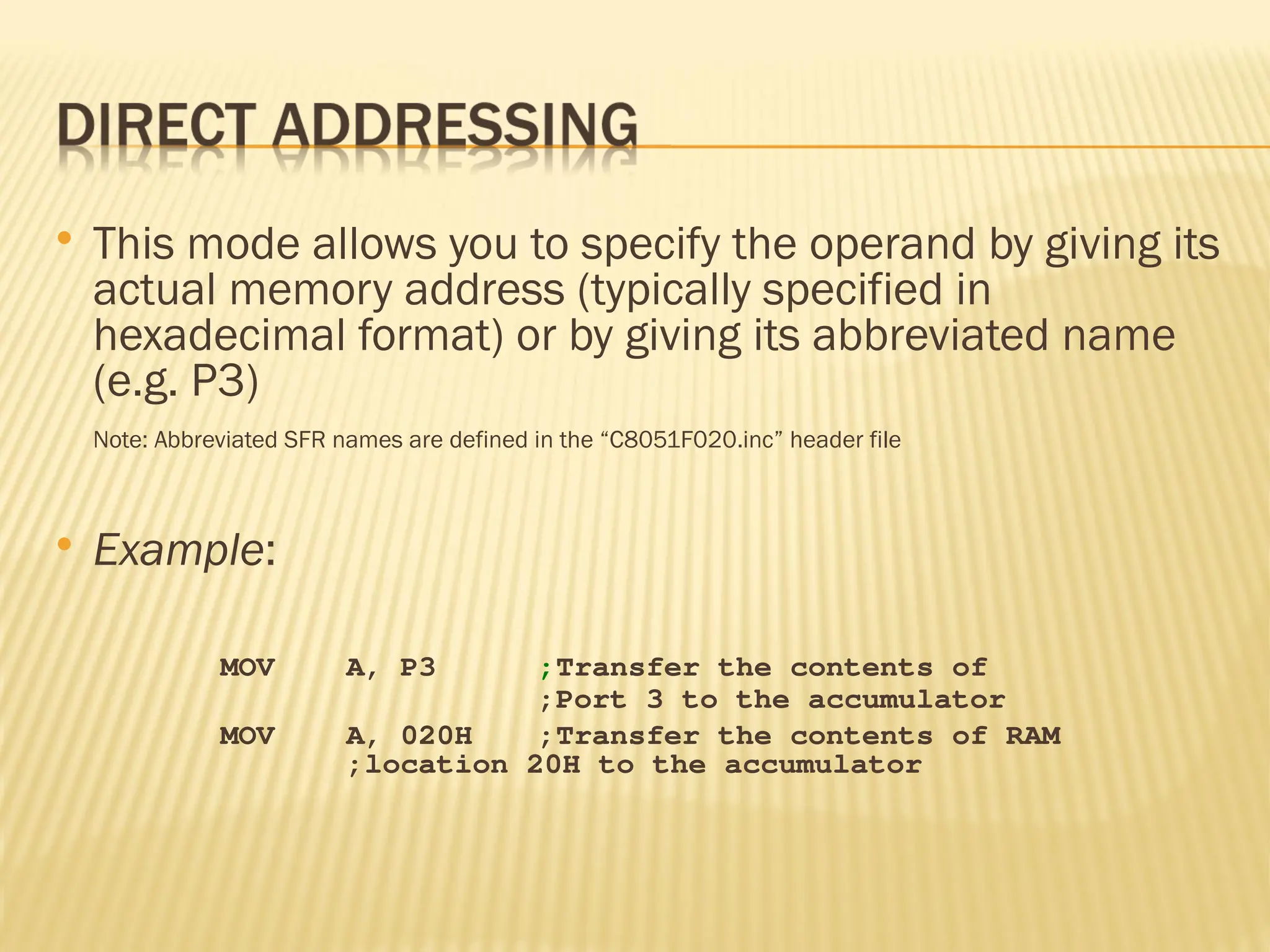
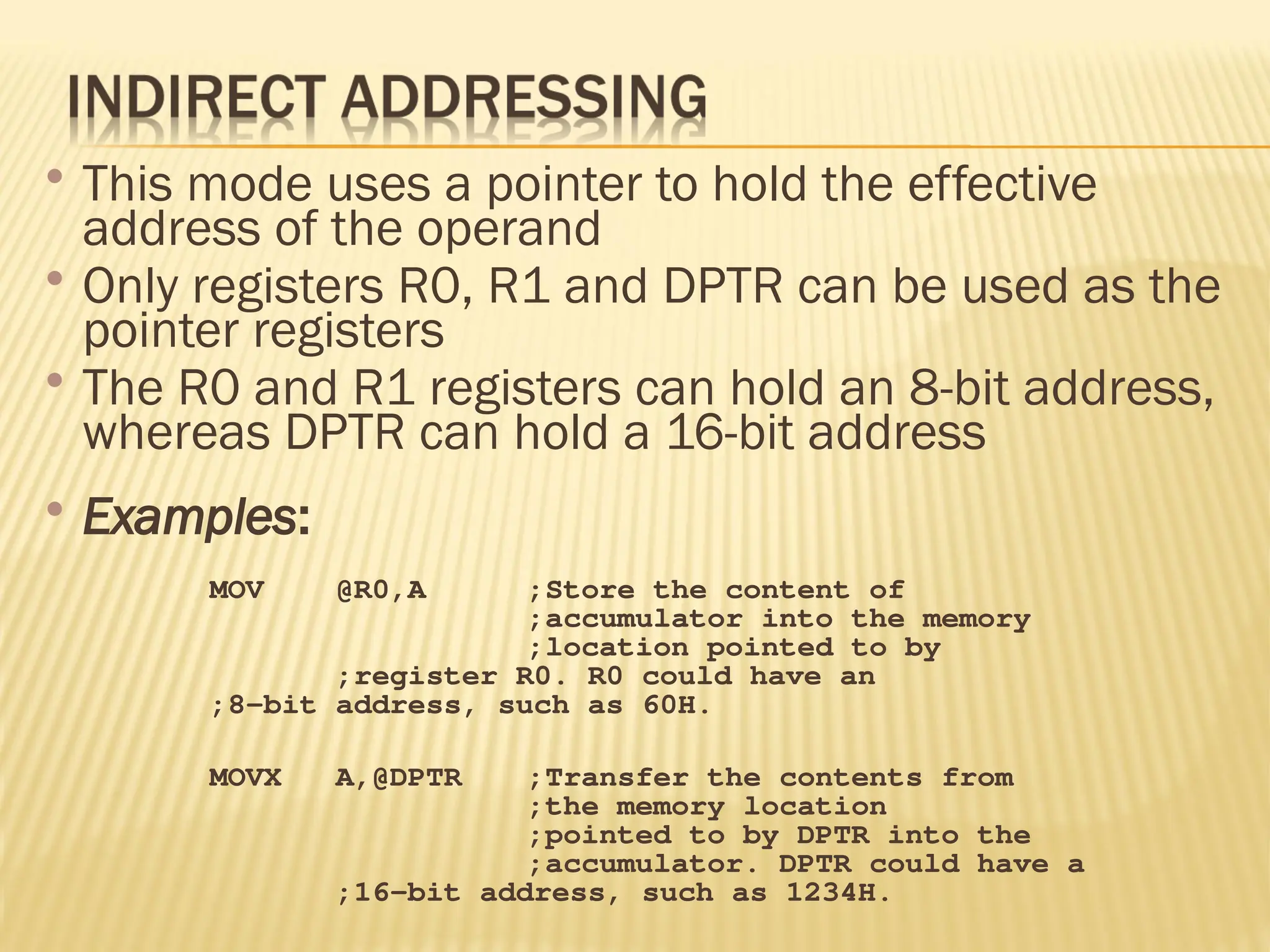
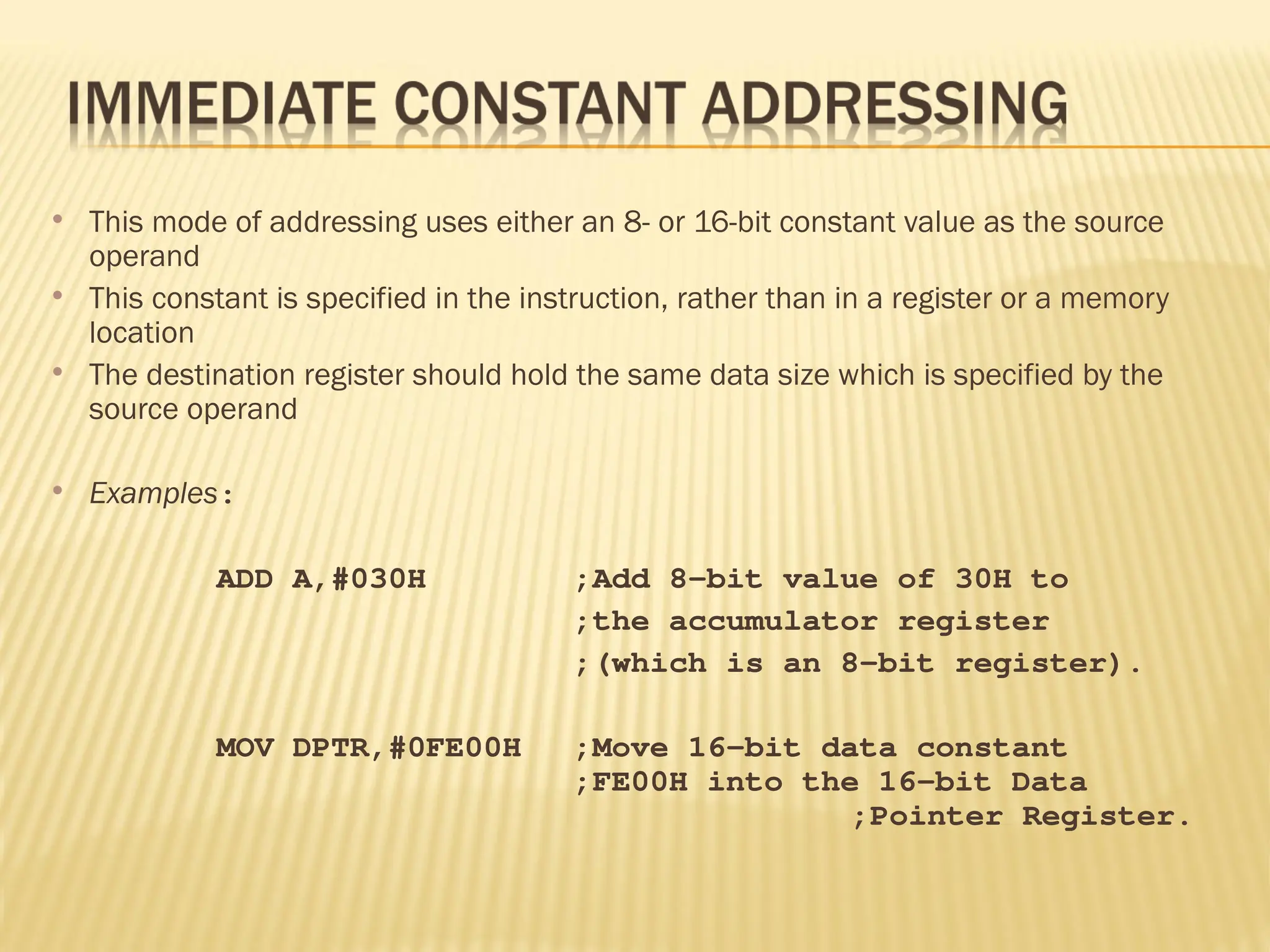
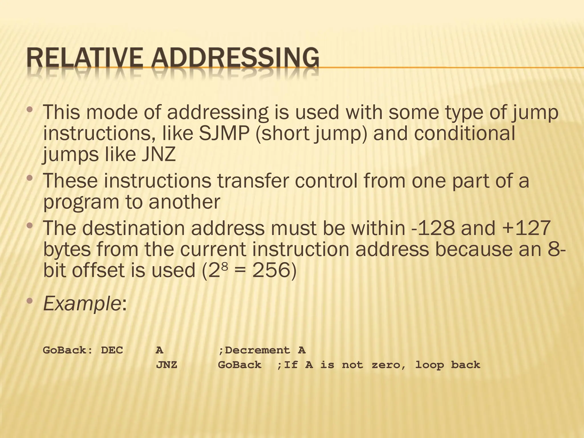
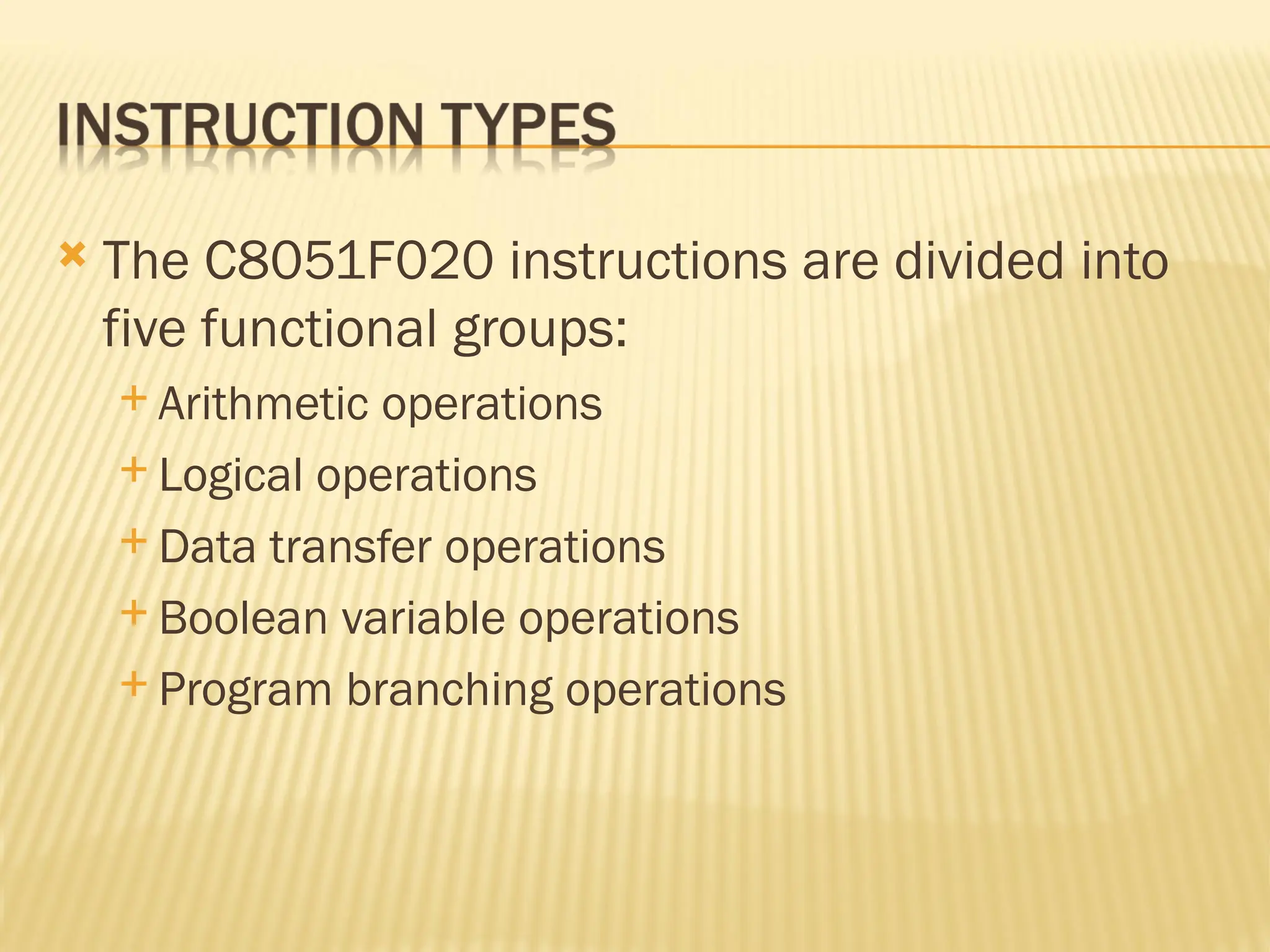
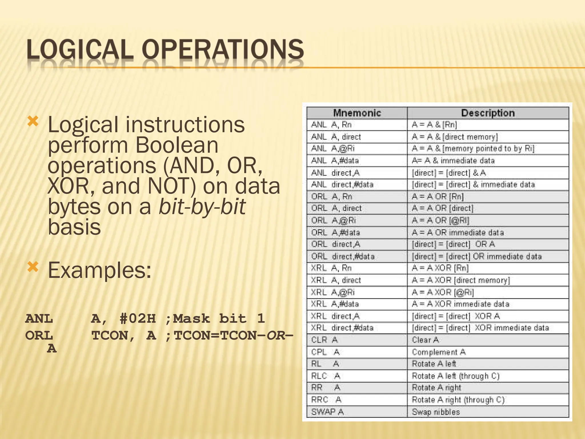
The document provides an overview of microprocessors and microcontrollers, emphasizing their roles in modern technology and embedded systems, detailing their components and characteristics. It includes a specific focus on the Intel 8051 microprocessor, its architecture, and functionality, along with addressing modes and additional hardware considerations. Key criteria for selecting microcontrollers are also discussed, including performance, software availability, and cost.
![ With arithmetic instructions, the C8051F020 CPU has no special knowledge of the data format (e.g. signed binary, unsigned binary, binary coded decimal, ASCII, etc.) The appropriate status bits in the PSW are set when specific conditions are met, which allows the user software to manage the different data formats [@Ri] implies contents of memory location pointed to by R0 or R1 Rn refers to registers R0-R7 of the currently selected register bank](https://image.slidesharecdn.com/8051microcontroller-240806023912-38e40e82/75/8051-Microcontroller-architecture-and-operation-51-2048.jpg)
![ Multiplies A & B and the 16-bit result stored in [B15-8], [A7-0] Multiplies the unsigned 8-bit integers in the accumulator and the B register The Low order byte of the 16-bit product will go to the accumulator and the High order byte will go to the B register If the product is greater than 255 (FFH), the overflow flag is set; otherwise it is cleared. The carry flag is always cleared. If ACC=85 (55H) and B=23 (17H), the instruction gives the product 1955 (07A3H), so B is now 07H and the accumulator is A3H. The overflow flag is set and the carry flag is cleared.](https://image.slidesharecdn.com/8051microcontroller-240806023912-38e40e82/75/8051-Microcontroller-architecture-and-operation-57-2048.jpg)
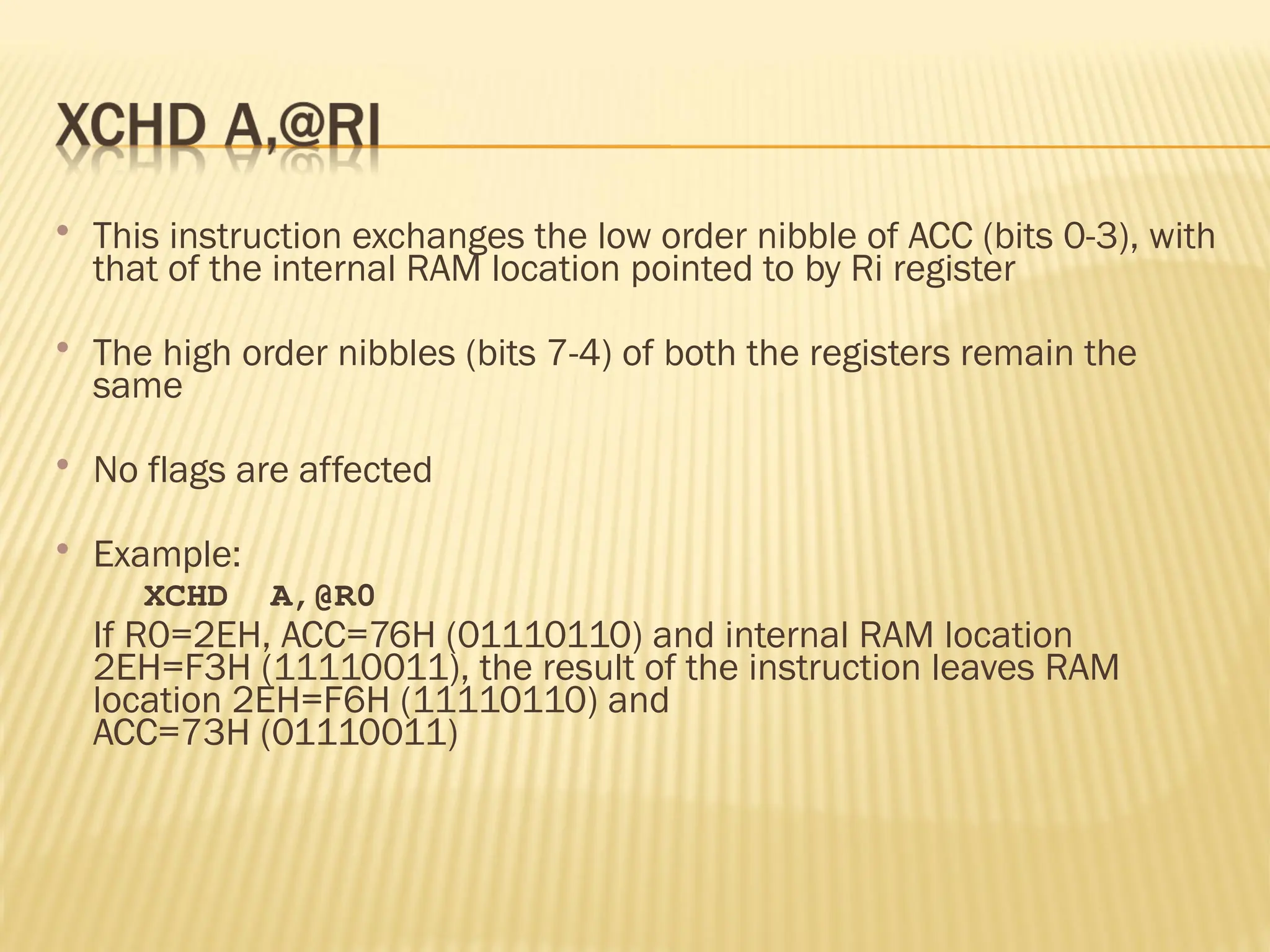
![ Data transfer instructions can be used to transfer data between an internal RAM location and an SFR location without going through the accumulator It is also possible to transfer data between the internal and external RAM by using indirect addressing The upper 128 bytes of data RAM are accessed only by indirect addressing and the SFRs are accessed only by direct addressing Mnemonic Description MOV @Ri, direct [@Ri] = [direct] MOV @Ri, #data [@Ri] = immediate data MOV DPTR, #data 16 [DPTR] = immediate data MOVC A,@A+DPTR A = Code byte from [@A+DPTR] MOVC A,@A+PC A = Code byte from [@A+PC] MOVX A,@Ri A = Data byte from external ram [@Ri] MOVX A,@DPTR A = Data byte from external ram [@DPTR] MOVX @Ri, A External[@Ri] = A MOVX @DPTR,A External[@DPTR] = A PUSH direct Push into stack POP direct Pop from stack XCH A,Rn A = [Rn], [Rn] = A XCH A, direct A = [direct], [direct] = A XCH A, @Ri A = [@Rn], [@Rn] = A XCHD A,@Ri Exchange low order digits](https://image.slidesharecdn.com/8051microcontroller-240806023912-38e40e82/75/8051-Microcontroller-architecture-and-operation-70-2048.jpg)
![ This instruction moves the source byte into the destination location The source byte is not affected, neither are any other registers or flags Example: MOV R1,#60 ;R1=60H MOV A,@R1 ;A=[60H] MOV R2,#61 ;R2=61H ADD A,@R2 ;A=A+[61H] MOV R7,A ;R7=A If internal RAM locations 60H=10H, and 61H=20H, then after the operations of the above instructions R7=A=30H. The data contents of memory locations 60H and 61H remain intact.](https://image.slidesharecdn.com/8051microcontroller-240806023912-38e40e82/75/8051-Microcontroller-architecture-and-operation-71-2048.jpg)
![ This instruction is ”decrement jump not zero” It decrements the contents of the destination location and if the resulting value is not 0, branches to the address indicated by the source operand An original value of 00H underflows to FFH No flags are affected Example: DJNZ 20H,LOC1 DJNZ 30H,LOC2 DJNZ 40H,LOC3 If internal RAM locations 20H, 30H and 40H contain the values 01H, 5FH and 16H respectively, the above instruction sequence will cause a jump to the instruction at LOC2, with the values 00H, 5EH, and 15H in the 3 RAM locations. Note, the first instruction will not branch to LOC1 because the [20H] = 00H, hence the program continues to the second instruction Only after the execution of the second instruction (where the location [30H] = 5FH), then the branching takes place](https://image.slidesharecdn.com/8051microcontroller-240806023912-38e40e82/75/8051-Microcontroller-architecture-and-operation-104-2048.jpg)