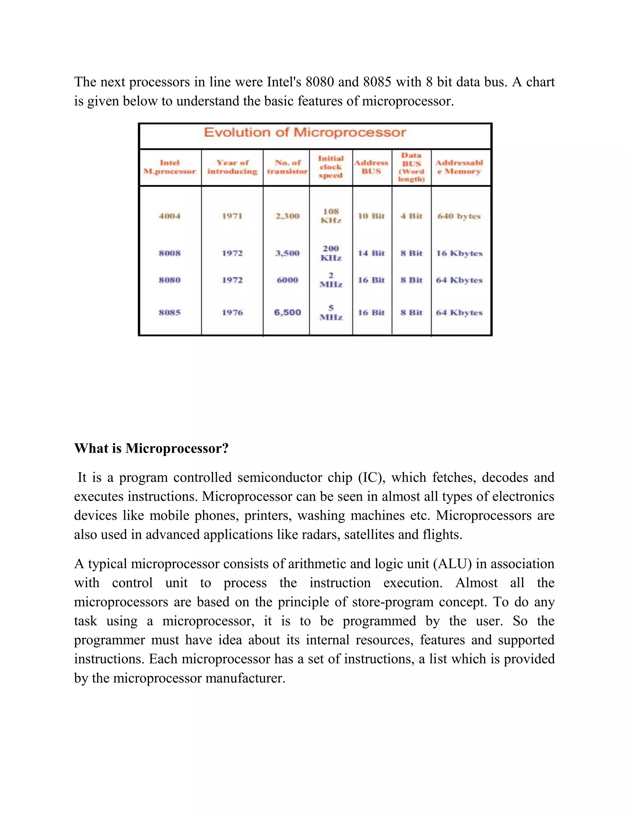
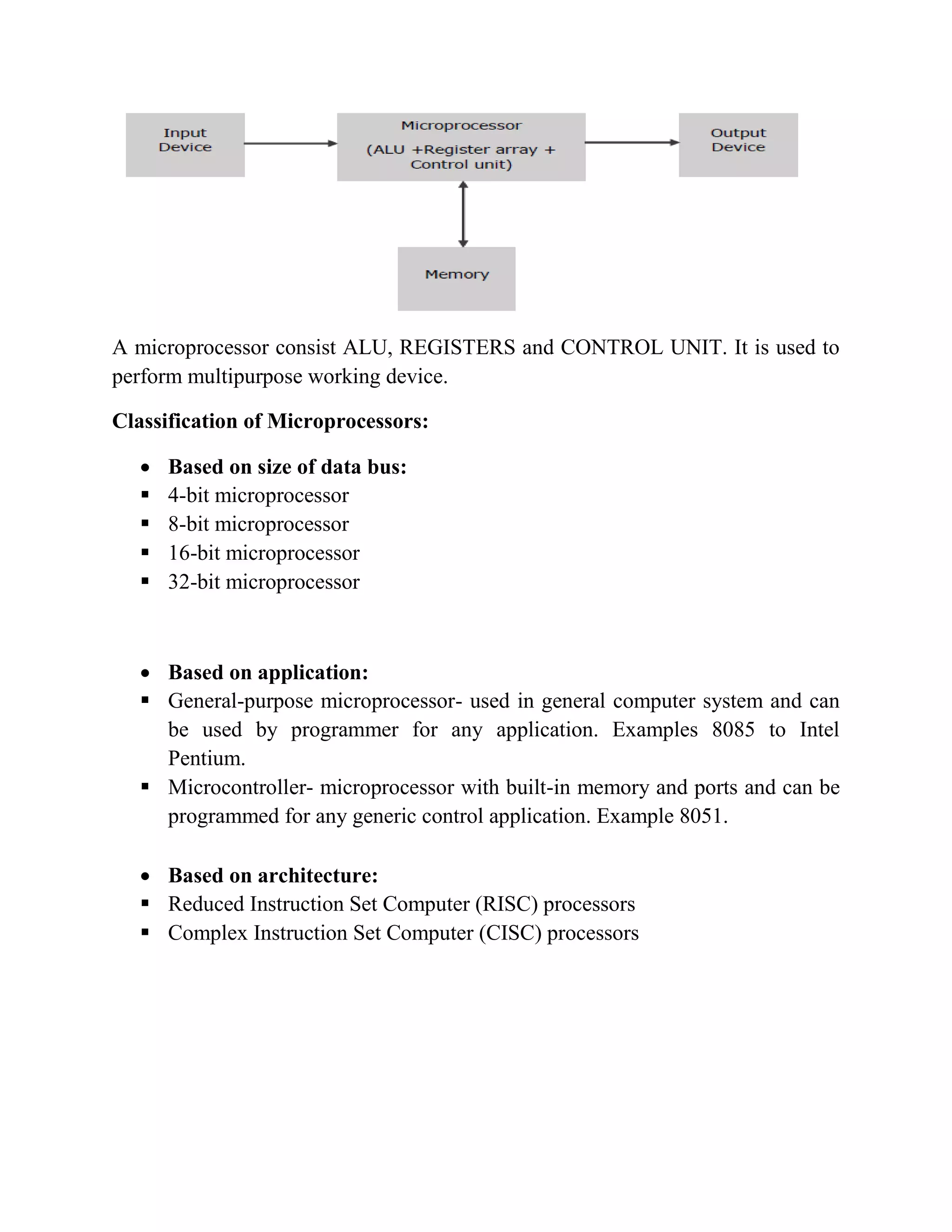
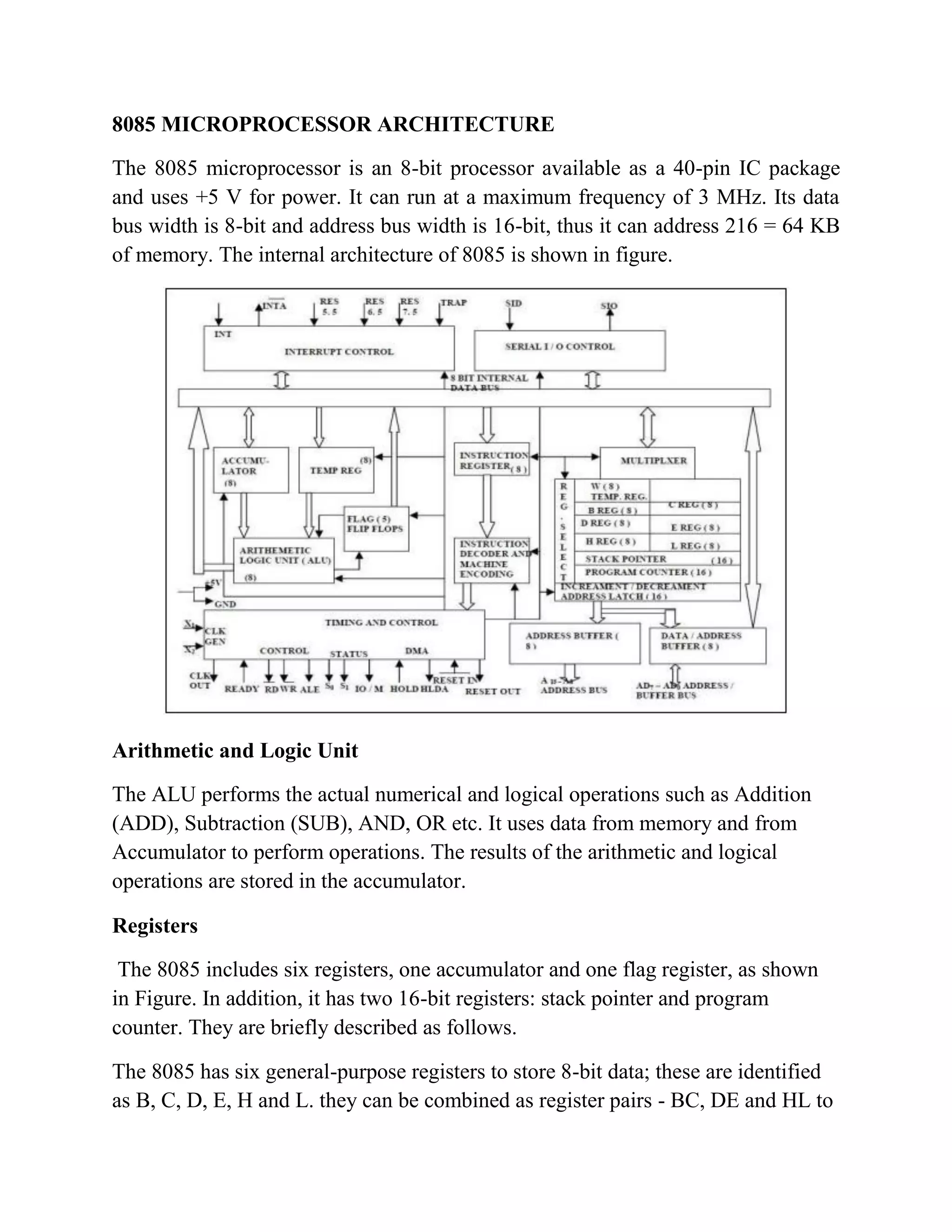
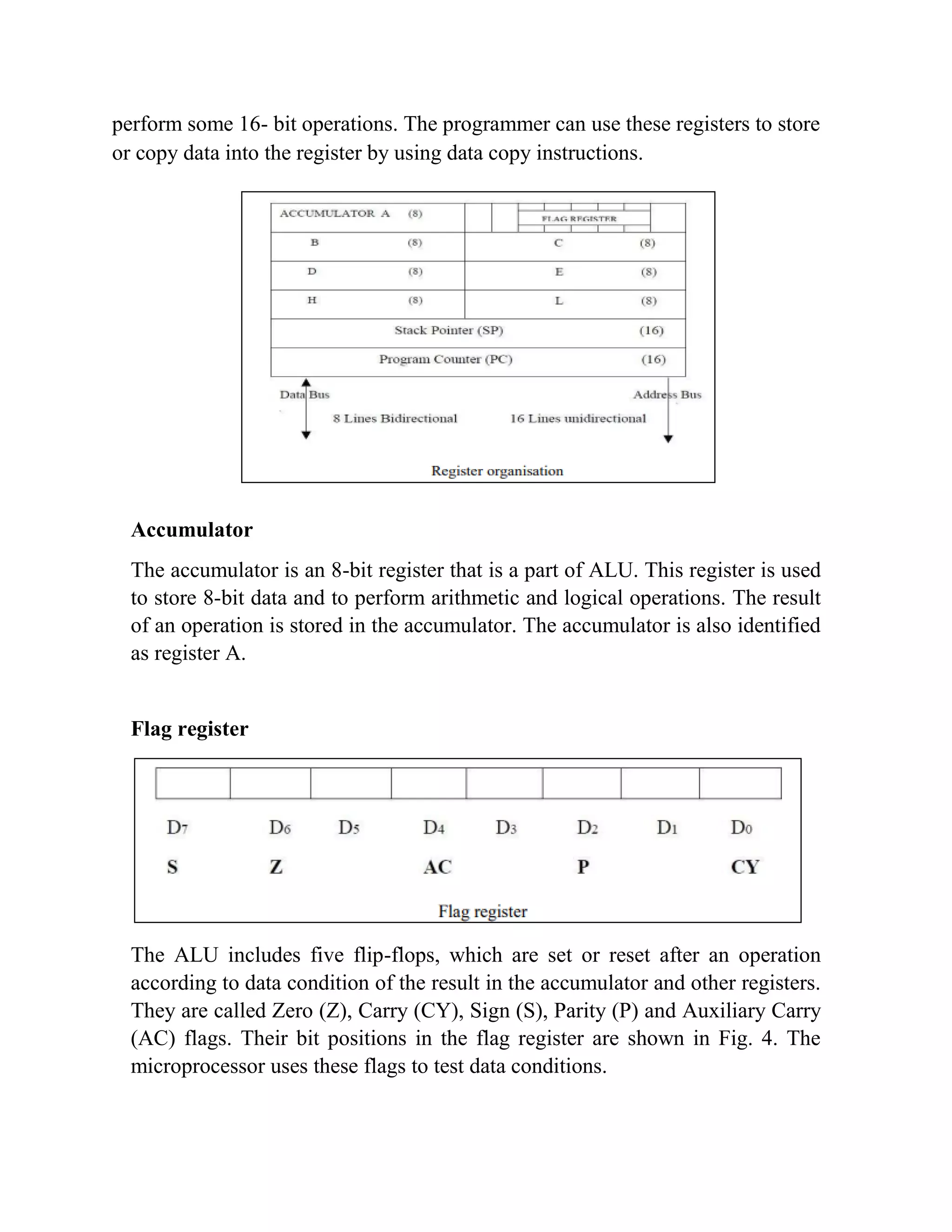
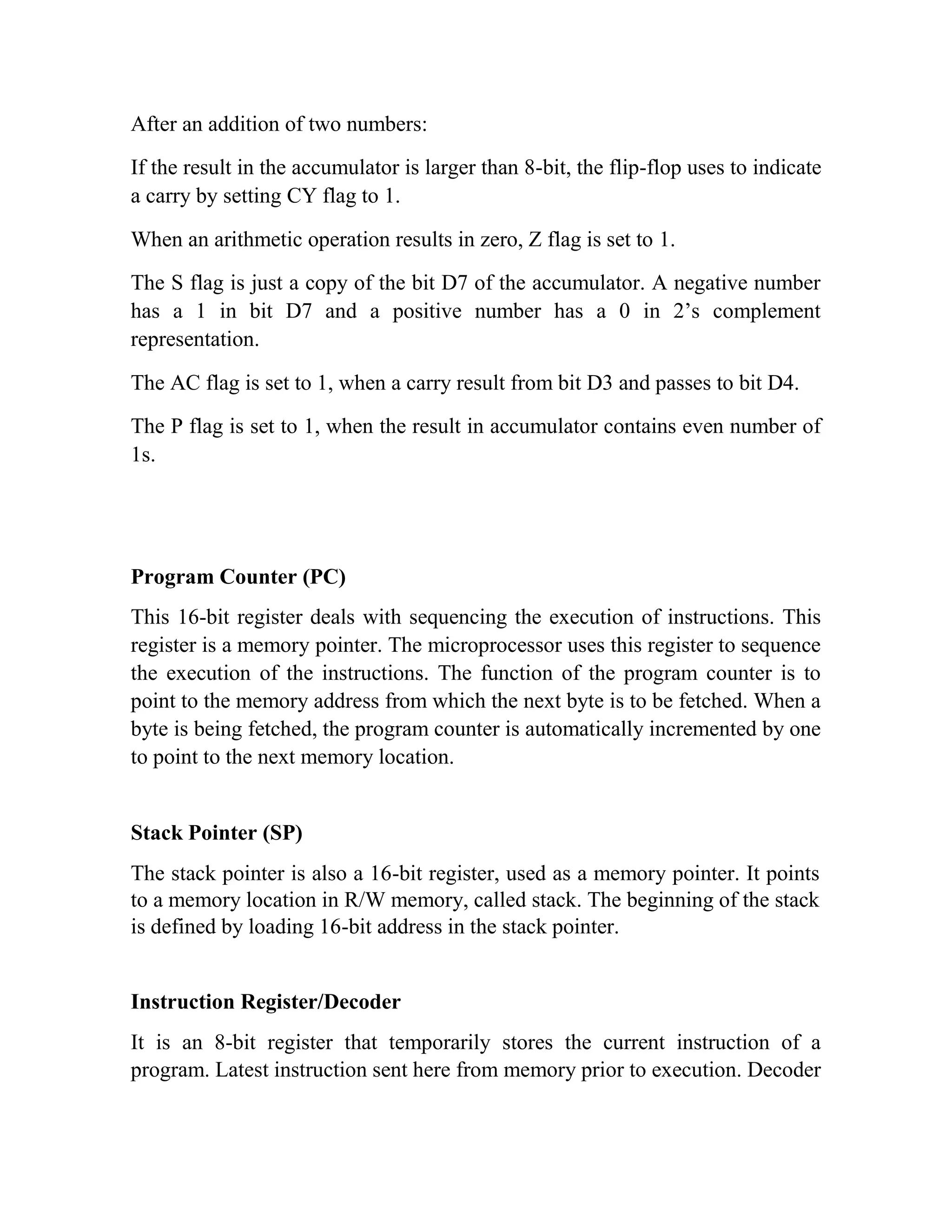
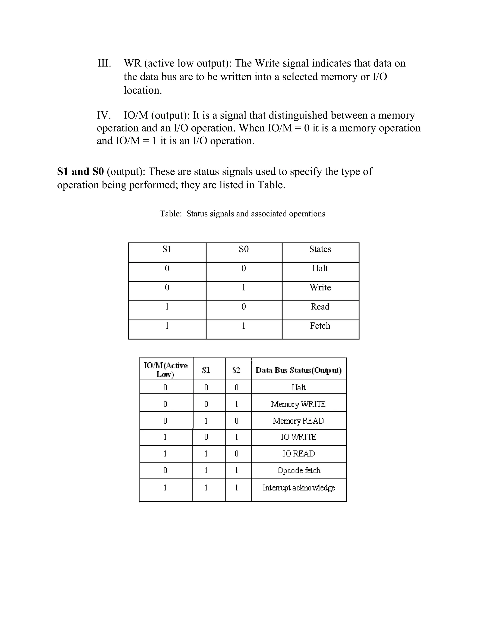
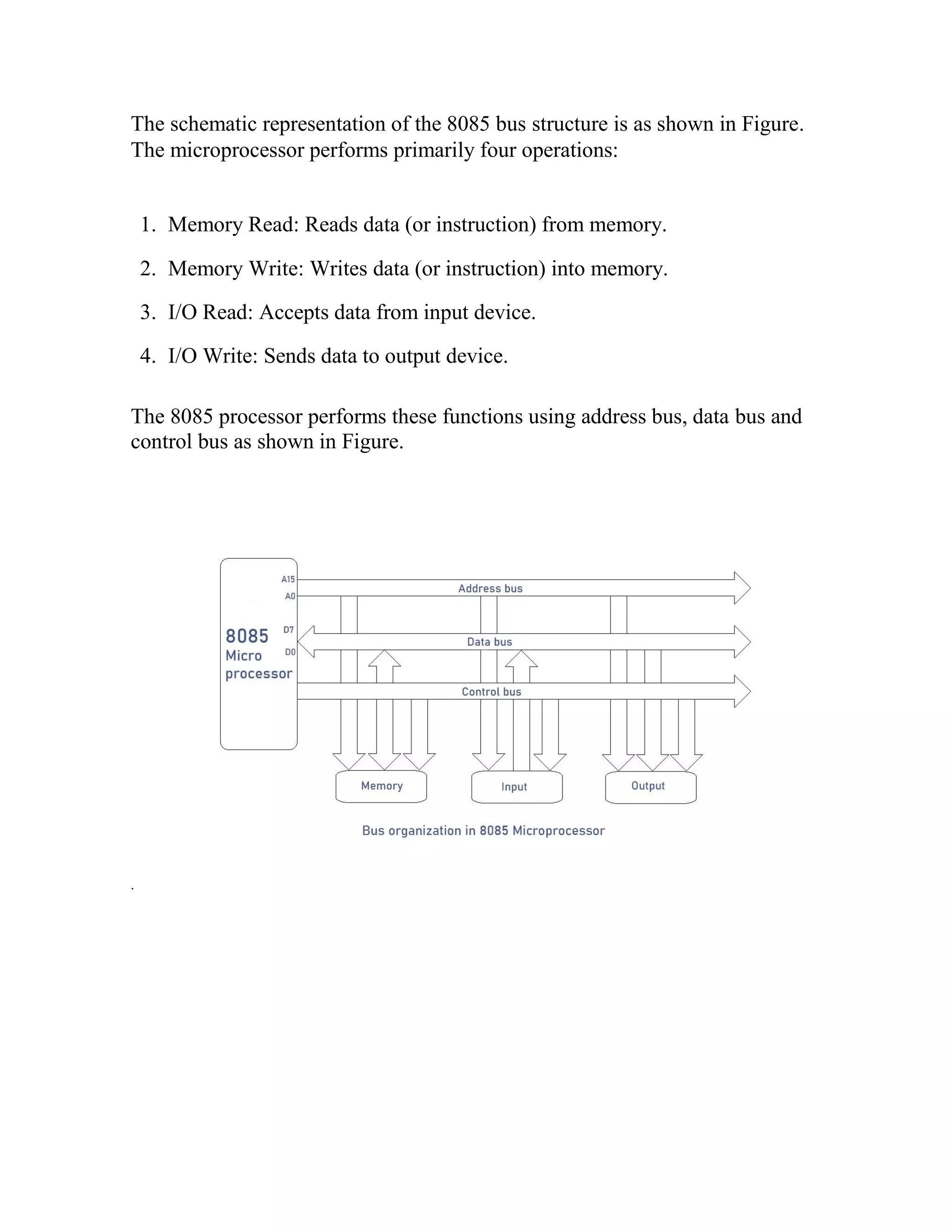
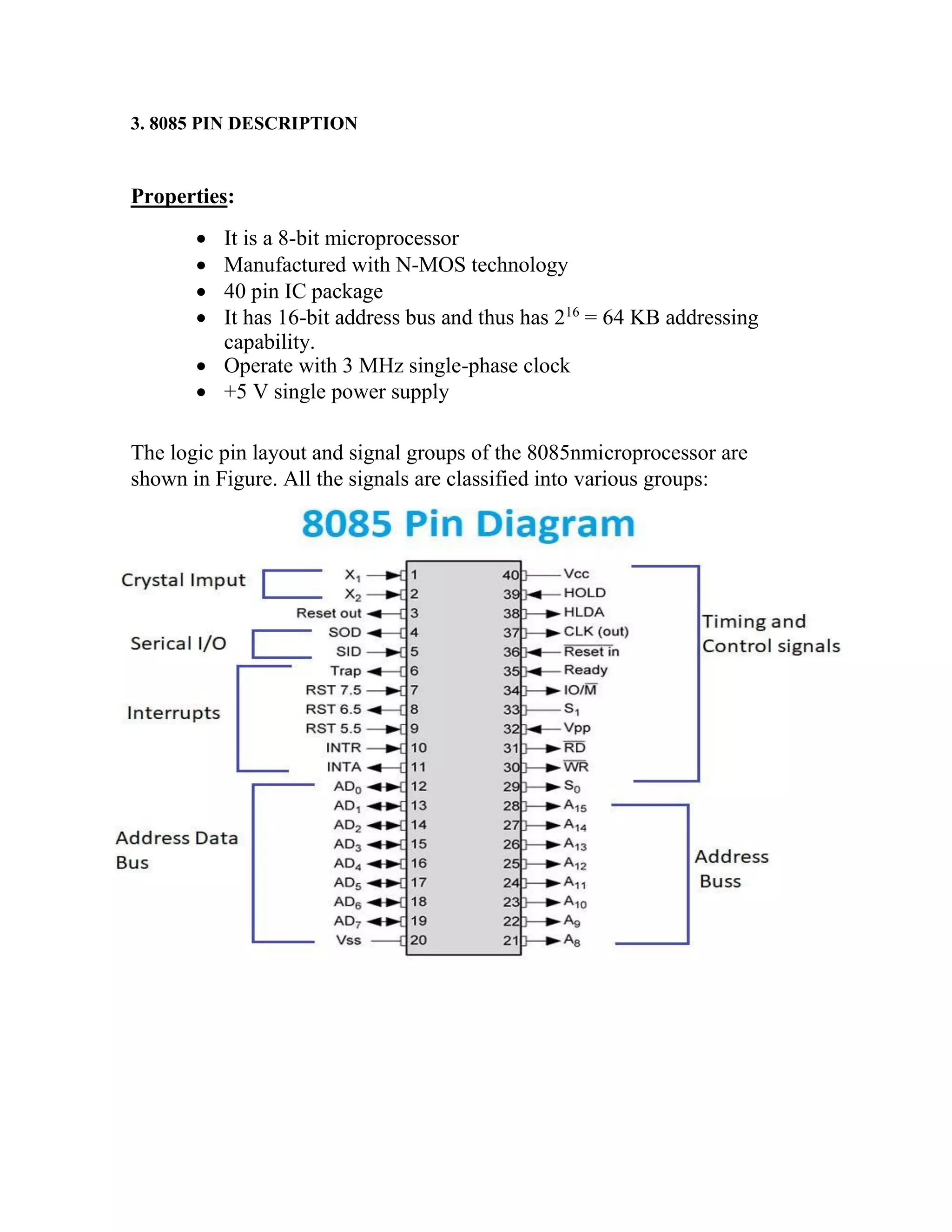
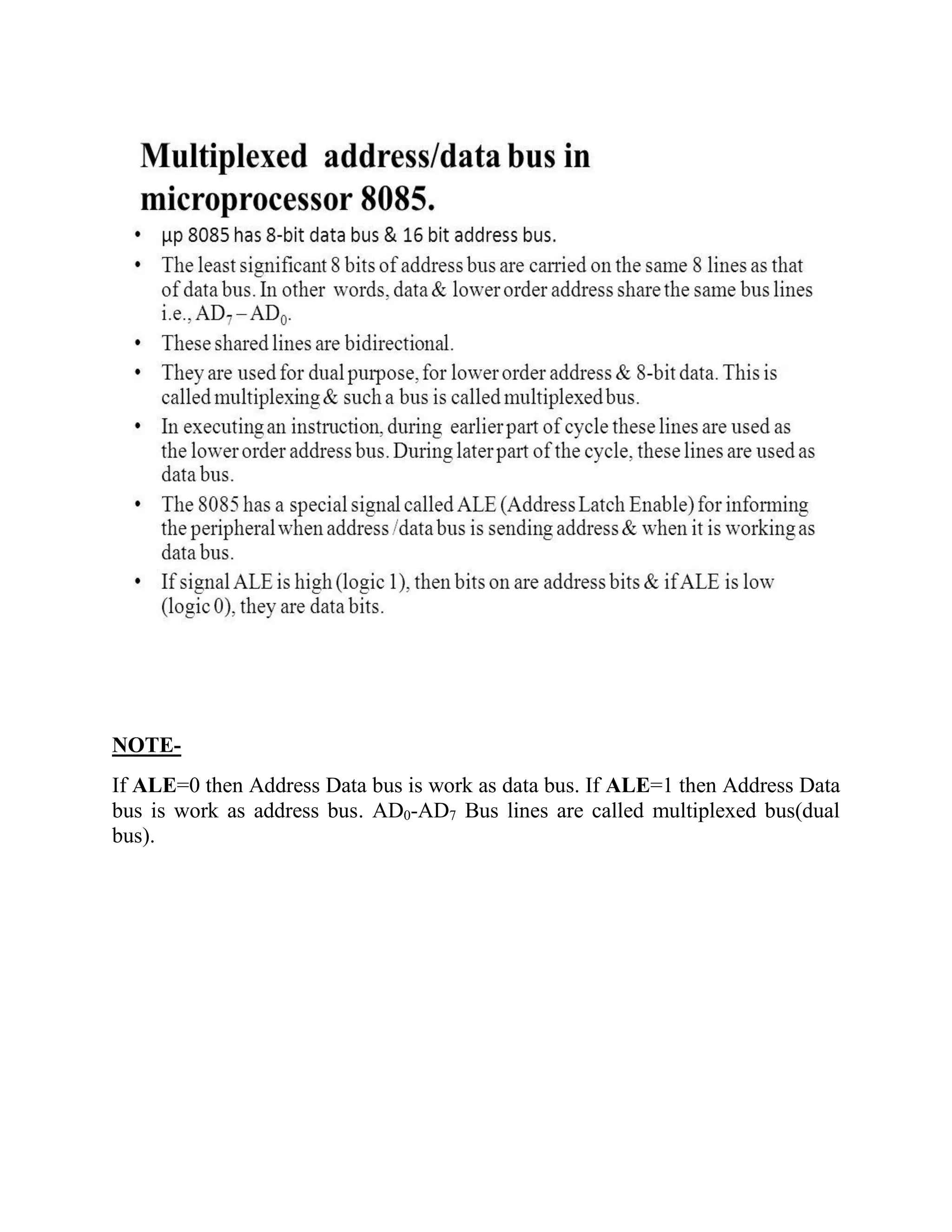
LECTURE NOTES ON MICROPROCESSOR and MICROCONTROLLER (Mr. SANDEEP GANGWAR) UNIT-1 History of microprocessor:- In 1947: Shockley, Brattain and Bardeen are credited with the invention of TRANSISTOR and were awarded the Nobel Prize for the same. A group of transistors arranged on a single platform, this platform, known as the integrated chip (IC). A person named JACK KILBY was honored with the Nobel Prize for the invention of IC, which laid the foundation on which microprocessors were developed. Complex developments in the IC led to the addition of more complex functions on a single chip. The stage was set for a single controlling circuit for all the computer functions. Finally, Intel Corporation’s were credited with the design of the first microprocessor. Intel 4004, the world's first microprocessor. The next in line was the 8 bit 8008 microprocessor. It was developed by Intel in 1972 to perform complex functions in harmony with the 4004.
The next processors in line were Intel's 8080 and 8085 with 8 bit data bus. A chart is given below to understand the basic features of microprocessor. What is Microprocessor? It is a program controlled semiconductor chip (IC), which fetches, decodes and executes instructions. Microprocessor can be seen in almost all types of electronics devices like mobile phones, printers, washing machines etc. Microprocessors are also used in advanced applications like radars, satellites and flights. A typical microprocessor consists of arithmetic and logic unit (ALU) in association with control unit to process the instruction execution. Almost all the microprocessors are based on the principle of store-program concept. To do any task using a microprocessor, it is to be programmed by the user. So the programmer must have idea about its internal resources, features and supported instructions. Each microprocessor has a set of instructions, a list which is provided by the microprocessor manufacturer.
A microprocessor consist ALU, REGISTERS and CONTROL UNIT. It is used to perform multipurpose working device. Classification of Microprocessors:  Based on size of data bus:  4-bit microprocessor  8-bit microprocessor  16-bit microprocessor  32-bit microprocessor  Based on application:  General-purpose microprocessor- used in general computer system and can be used by programmer for any application. Examples 8085 to Intel Pentium.  Microcontroller- microprocessor with built-in memory and ports and can be programmed for any generic control application. Example 8051.  Based on architecture:  Reduced Instruction Set Computer (RISC) processors  Complex Instruction Set Computer (CISC) processors
8085 MICROPROCESSOR ARCHITECTURE The 8085 microprocessor is an 8-bit processor available as a 40-pin IC package and uses +5 V for power. It can run at a maximum frequency of 3 MHz. Its data bus width is 8-bit and address bus width is 16-bit, thus it can address 216 = 64 KB of memory. The internal architecture of 8085 is shown in figure. Arithmetic and Logic Unit The ALU performs the actual numerical and logical operations such as Addition (ADD), Subtraction (SUB), AND, OR etc. It uses data from memory and from Accumulator to perform operations. The results of the arithmetic and logical operations are stored in the accumulator. Registers The 8085 includes six registers, one accumulator and one flag register, as shown in Figure. In addition, it has two 16-bit registers: stack pointer and program counter. They are briefly described as follows. The 8085 has six general-purpose registers to store 8-bit data; these are identified as B, C, D, E, H and L. they can be combined as register pairs - BC, DE and HL to
perform some 16- bit operations. The programmer can use these registers to store or copy data into the register by using data copy instructions. Accumulator The accumulator is an 8-bit register that is a part of ALU. This register is used to store 8-bit data and to perform arithmetic and logical operations. The result of an operation is stored in the accumulator. The accumulator is also identified as register A. Flag register The ALU includes five flip-flops, which are set or reset after an operation according to data condition of the result in the accumulator and other registers. They are called Zero (Z), Carry (CY), Sign (S), Parity (P) and Auxiliary Carry (AC) flags. Their bit positions in the flag register are shown in Fig. 4. The microprocessor uses these flags to test data conditions.
After an addition of two numbers: If the result in the accumulator is larger than 8-bit, the flip-flop uses to indicate a carry by setting CY flag to 1. When an arithmetic operation results in zero, Z flag is set to 1. The S flag is just a copy of the bit D7 of the accumulator. A negative number has a 1 in bit D7 and a positive number has a 0 in 2’s complement representation. The AC flag is set to 1, when a carry result from bit D3 and passes to bit D4. The P flag is set to 1, when the result in accumulator contains even number of 1s. Program Counter (PC) This 16-bit register deals with sequencing the execution of instructions. This register is a memory pointer. The microprocessor uses this register to sequence the execution of the instructions. The function of the program counter is to point to the memory address from which the next byte is to be fetched. When a byte is being fetched, the program counter is automatically incremented by one to point to the next memory location. Stack Pointer (SP) The stack pointer is also a 16-bit register, used as a memory pointer. It points to a memory location in R/W memory, called stack. The beginning of the stack is defined by loading 16-bit address in the stack pointer. Instruction Register/Decoder It is an 8-bit register that temporarily stores the current instruction of a program. Latest instruction sent here from memory prior to execution. Decoder
then takes instruction and decodes or interprets the instruction. Decoded instruction then passed to next stage. Control Unit Generates signals on data bus, address bus and control bus within microprocessor to carry out the instruction, which has been decoded. Typical buses and their timing are described as follows: Data Bus: Data bus carries data in binary form between microprocessor and other external units such as memory. It is used to transmit data i.e. information, results of arithmetic etc between memory and the microprocessor. Data bus is bidirectional in nature. The data bus width of 8085 microprocessor is 8-bit i.e. 28 combination of binary digits and are typically identified as D0 – D7. Thus size of the data bus determines what arithmetic can be done. If only 8-bit wide then largest number is 11111111 (255 in decimal). Therefore, larger numbers have to be broken down into chunks of 255. This slows microprocessor. Address Bus: The address bus carries addresses and is one way bus from microprocessor to the memory or other devices. 8085 microprocessor contain 16-bit address bus and are generally identified as A0 - A15. The higher order address lines (A8 – A15) are unidirectional and the lower order lines (A0 – A7) are multiplexed (time-shared) with the eight data bits (D0 – D7) and hence, they are bidirectional. Control Bus: Control bus are various lines which have specific functions for coordinating and controlling microprocessor operations. The control bus carries control signals partly unidirectional and partly bidirectional. The following control and status signals are used by 8085 processor: I. ALE (output): Address Latch Enable is a pulse that is provided when an address appears on the AD0 – AD7 lines, after which it becomes 0. II. RD (active low output): The Read signal indicates that data are being read from the selected I/O or memory device and that they are available on the data bus.
III. WR (active low output): The Write signal indicates that data on the data bus are to be written into a selected memory or I/O location. IV. IO/M (output): It is a signal that distinguished between a memory operation and an I/O operation. When IO/M = 0 it is a memory operation and IO/M = 1 it is an I/O operation. S1 and S0 (output): These are status signals used to specify the type of operation being performed; they are listed in Table. Table: Status signals and associated operations S1 S0 States 0 0 Halt 0 1 Write 1 0 Read 1 1 Fetch
The schematic representation of the 8085 bus structure is as shown in Figure. The microprocessor performs primarily four operations: 1. Memory Read: Reads data (or instruction) from memory. 2. Memory Write: Writes data (or instruction) into memory. 3. I/O Read: Accepts data from input device. 4. I/O Write: Sends data to output device. The 8085 processor performs these functions using address bus, data bus and control bus as shown in Figure. .
3. 8085 PIN DESCRIPTION Properties:  It is a 8-bit microprocessor  Manufactured with N-MOS technology  40 pin IC package  It has 16-bit address bus and thus has 216 = 64 KB addressing capability.  Operate with 3 MHz single-phase clock  +5 V single power supply The logic pin layout and signal groups of the 8085nmicroprocessor are shown in Figure. All the signals are classified into various groups:
Address and Data Buses: A8 – A15 (output, 3-state): Most significant eight bits of memory addresses and the eight bits of the I/O addresses. These lines enter into tri-state high impedance state during HOLD and HALT modes. AD0 – AD7 (input/output, 3-state): Lower significant bits of memory addresses and the eight bits of the I/O addresses during first clock. Control & Status Signals: ALE: Address latch enable RD : Read control signal. WR : Write control signal. IO/M : Input Output/ Memory S1 and S0 : Status signals. Supply & Clock Frequency: Vcc: +5 V power supply Vss: Ground reference X1, X2: A crystal having frequency of 6 MHz is connected at these two pins CLK: Clock output
Externally Initiated and Interrupt Signals: RESET IN : When the signal on this pin is low, the PC is set to 0, the buses are tri-stated and the processor is reset. RESET OUT: This signal indicates that the processor is being reset. The signal can be used to reset other devices. READY: When this signal is low, the processor waits for an integral number of clock cycles until it goes high. HOLD: This signal indicates that a peripheral like DMA (direct memory access) controller is requesting the use of address and data bus. HLDA: This signal acknowledges the HOLD request. INTR: Interrupt request is a general-purpose interrupt. INTA : This is used to acknowledge an interrupt. RST 7.5, RST 6.5, RST 5.5 – restart interrupt: These are vectored interrupts and have highest priority than INTR interrupt. TRAP: This is a non-maskable interrupt and has the highest priority. Serial I/O Signals: SID: Serial input signal. Bit on this line is loaded to D7 bit of register A using RIM instruction. SOD: Serial output signal. Output SOD is set or reset by using SIM instruction.
NOTE- If ALE=0 then Address Data bus is work as data bus. If ALE=1 then Address Data bus is work as address bus. AD0-AD7 Bus lines are called multiplexed bus(dual bus).

MPMC UNIT-1. Microprocessor 8085 pdf Microprocessor and Microcontroller

  • 1.
    LECTURE NOTES ON MICROPROCESSOR andMICROCONTROLLER (Mr. SANDEEP GANGWAR) UNIT-1 History of microprocessor:- In 1947: Shockley, Brattain and Bardeen are credited with the invention of TRANSISTOR and were awarded the Nobel Prize for the same. A group of transistors arranged on a single platform, this platform, known as the integrated chip (IC). A person named JACK KILBY was honored with the Nobel Prize for the invention of IC, which laid the foundation on which microprocessors were developed. Complex developments in the IC led to the addition of more complex functions on a single chip. The stage was set for a single controlling circuit for all the computer functions. Finally, Intel Corporation’s were credited with the design of the first microprocessor. Intel 4004, the world's first microprocessor. The next in line was the 8 bit 8008 microprocessor. It was developed by Intel in 1972 to perform complex functions in harmony with the 4004.
  • 2.
    The next processorsin line were Intel's 8080 and 8085 with 8 bit data bus. A chart is given below to understand the basic features of microprocessor. What is Microprocessor? It is a program controlled semiconductor chip (IC), which fetches, decodes and executes instructions. Microprocessor can be seen in almost all types of electronics devices like mobile phones, printers, washing machines etc. Microprocessors are also used in advanced applications like radars, satellites and flights. A typical microprocessor consists of arithmetic and logic unit (ALU) in association with control unit to process the instruction execution. Almost all the microprocessors are based on the principle of store-program concept. To do any task using a microprocessor, it is to be programmed by the user. So the programmer must have idea about its internal resources, features and supported instructions. Each microprocessor has a set of instructions, a list which is provided by the microprocessor manufacturer.
  • 3.
    A microprocessor consistALU, REGISTERS and CONTROL UNIT. It is used to perform multipurpose working device. Classification of Microprocessors:  Based on size of data bus:  4-bit microprocessor  8-bit microprocessor  16-bit microprocessor  32-bit microprocessor  Based on application:  General-purpose microprocessor- used in general computer system and can be used by programmer for any application. Examples 8085 to Intel Pentium.  Microcontroller- microprocessor with built-in memory and ports and can be programmed for any generic control application. Example 8051.  Based on architecture:  Reduced Instruction Set Computer (RISC) processors  Complex Instruction Set Computer (CISC) processors
  • 4.
    8085 MICROPROCESSOR ARCHITECTURE The8085 microprocessor is an 8-bit processor available as a 40-pin IC package and uses +5 V for power. It can run at a maximum frequency of 3 MHz. Its data bus width is 8-bit and address bus width is 16-bit, thus it can address 216 = 64 KB of memory. The internal architecture of 8085 is shown in figure. Arithmetic and Logic Unit The ALU performs the actual numerical and logical operations such as Addition (ADD), Subtraction (SUB), AND, OR etc. It uses data from memory and from Accumulator to perform operations. The results of the arithmetic and logical operations are stored in the accumulator. Registers The 8085 includes six registers, one accumulator and one flag register, as shown in Figure. In addition, it has two 16-bit registers: stack pointer and program counter. They are briefly described as follows. The 8085 has six general-purpose registers to store 8-bit data; these are identified as B, C, D, E, H and L. they can be combined as register pairs - BC, DE and HL to
  • 5.
    perform some 16-bit operations. The programmer can use these registers to store or copy data into the register by using data copy instructions. Accumulator The accumulator is an 8-bit register that is a part of ALU. This register is used to store 8-bit data and to perform arithmetic and logical operations. The result of an operation is stored in the accumulator. The accumulator is also identified as register A. Flag register The ALU includes five flip-flops, which are set or reset after an operation according to data condition of the result in the accumulator and other registers. They are called Zero (Z), Carry (CY), Sign (S), Parity (P) and Auxiliary Carry (AC) flags. Their bit positions in the flag register are shown in Fig. 4. The microprocessor uses these flags to test data conditions.
  • 6.
    After an additionof two numbers: If the result in the accumulator is larger than 8-bit, the flip-flop uses to indicate a carry by setting CY flag to 1. When an arithmetic operation results in zero, Z flag is set to 1. The S flag is just a copy of the bit D7 of the accumulator. A negative number has a 1 in bit D7 and a positive number has a 0 in 2’s complement representation. The AC flag is set to 1, when a carry result from bit D3 and passes to bit D4. The P flag is set to 1, when the result in accumulator contains even number of 1s. Program Counter (PC) This 16-bit register deals with sequencing the execution of instructions. This register is a memory pointer. The microprocessor uses this register to sequence the execution of the instructions. The function of the program counter is to point to the memory address from which the next byte is to be fetched. When a byte is being fetched, the program counter is automatically incremented by one to point to the next memory location. Stack Pointer (SP) The stack pointer is also a 16-bit register, used as a memory pointer. It points to a memory location in R/W memory, called stack. The beginning of the stack is defined by loading 16-bit address in the stack pointer. Instruction Register/Decoder It is an 8-bit register that temporarily stores the current instruction of a program. Latest instruction sent here from memory prior to execution. Decoder
  • 7.
    then takes instructionand decodes or interprets the instruction. Decoded instruction then passed to next stage. Control Unit Generates signals on data bus, address bus and control bus within microprocessor to carry out the instruction, which has been decoded. Typical buses and their timing are described as follows: Data Bus: Data bus carries data in binary form between microprocessor and other external units such as memory. It is used to transmit data i.e. information, results of arithmetic etc between memory and the microprocessor. Data bus is bidirectional in nature. The data bus width of 8085 microprocessor is 8-bit i.e. 28 combination of binary digits and are typically identified as D0 – D7. Thus size of the data bus determines what arithmetic can be done. If only 8-bit wide then largest number is 11111111 (255 in decimal). Therefore, larger numbers have to be broken down into chunks of 255. This slows microprocessor. Address Bus: The address bus carries addresses and is one way bus from microprocessor to the memory or other devices. 8085 microprocessor contain 16-bit address bus and are generally identified as A0 - A15. The higher order address lines (A8 – A15) are unidirectional and the lower order lines (A0 – A7) are multiplexed (time-shared) with the eight data bits (D0 – D7) and hence, they are bidirectional. Control Bus: Control bus are various lines which have specific functions for coordinating and controlling microprocessor operations. The control bus carries control signals partly unidirectional and partly bidirectional. The following control and status signals are used by 8085 processor: I. ALE (output): Address Latch Enable is a pulse that is provided when an address appears on the AD0 – AD7 lines, after which it becomes 0. II. RD (active low output): The Read signal indicates that data are being read from the selected I/O or memory device and that they are available on the data bus.
  • 8.
    III. WR (activelow output): The Write signal indicates that data on the data bus are to be written into a selected memory or I/O location. IV. IO/M (output): It is a signal that distinguished between a memory operation and an I/O operation. When IO/M = 0 it is a memory operation and IO/M = 1 it is an I/O operation. S1 and S0 (output): These are status signals used to specify the type of operation being performed; they are listed in Table. Table: Status signals and associated operations S1 S0 States 0 0 Halt 0 1 Write 1 0 Read 1 1 Fetch
  • 9.
    The schematic representationof the 8085 bus structure is as shown in Figure. The microprocessor performs primarily four operations: 1. Memory Read: Reads data (or instruction) from memory. 2. Memory Write: Writes data (or instruction) into memory. 3. I/O Read: Accepts data from input device. 4. I/O Write: Sends data to output device. The 8085 processor performs these functions using address bus, data bus and control bus as shown in Figure. .
  • 10.
    3. 8085 PINDESCRIPTION Properties:  It is a 8-bit microprocessor  Manufactured with N-MOS technology  40 pin IC package  It has 16-bit address bus and thus has 216 = 64 KB addressing capability.  Operate with 3 MHz single-phase clock  +5 V single power supply The logic pin layout and signal groups of the 8085nmicroprocessor are shown in Figure. All the signals are classified into various groups:
  • 11.
    Address and DataBuses: A8 – A15 (output, 3-state): Most significant eight bits of memory addresses and the eight bits of the I/O addresses. These lines enter into tri-state high impedance state during HOLD and HALT modes. AD0 – AD7 (input/output, 3-state): Lower significant bits of memory addresses and the eight bits of the I/O addresses during first clock. Control & Status Signals: ALE: Address latch enable RD : Read control signal. WR : Write control signal. IO/M : Input Output/ Memory S1 and S0 : Status signals. Supply & Clock Frequency: Vcc: +5 V power supply Vss: Ground reference X1, X2: A crystal having frequency of 6 MHz is connected at these two pins CLK: Clock output
  • 12.
    Externally Initiated andInterrupt Signals: RESET IN : When the signal on this pin is low, the PC is set to 0, the buses are tri-stated and the processor is reset. RESET OUT: This signal indicates that the processor is being reset. The signal can be used to reset other devices. READY: When this signal is low, the processor waits for an integral number of clock cycles until it goes high. HOLD: This signal indicates that a peripheral like DMA (direct memory access) controller is requesting the use of address and data bus. HLDA: This signal acknowledges the HOLD request. INTR: Interrupt request is a general-purpose interrupt. INTA : This is used to acknowledge an interrupt. RST 7.5, RST 6.5, RST 5.5 – restart interrupt: These are vectored interrupts and have highest priority than INTR interrupt. TRAP: This is a non-maskable interrupt and has the highest priority. Serial I/O Signals: SID: Serial input signal. Bit on this line is loaded to D7 bit of register A using RIM instruction. SOD: Serial output signal. Output SOD is set or reset by using SIM instruction.
  • 13.
    NOTE- If ALE=0 thenAddress Data bus is work as data bus. If ALE=1 then Address Data bus is work as address bus. AD0-AD7 Bus lines are called multiplexed bus(dual bus).