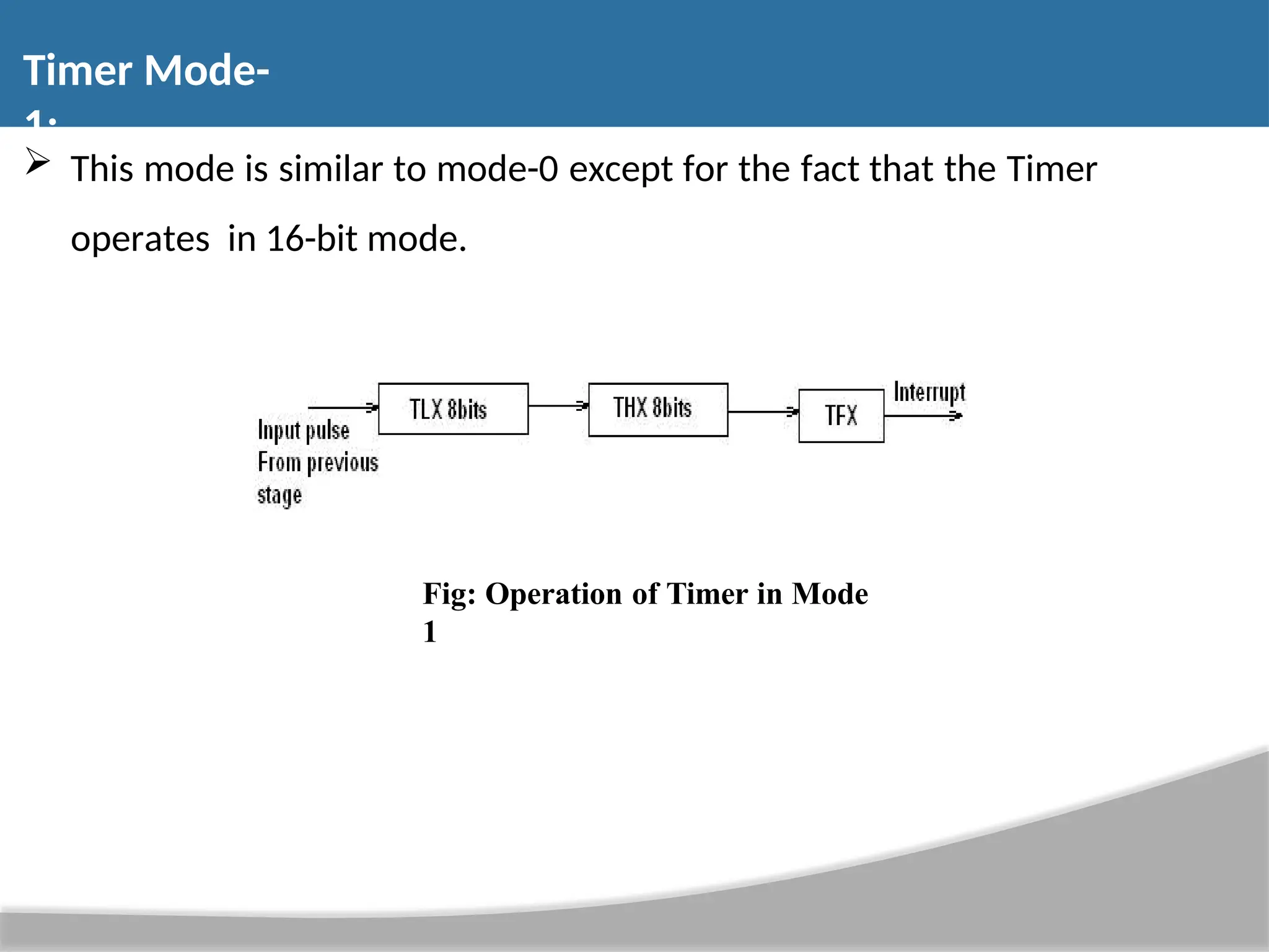
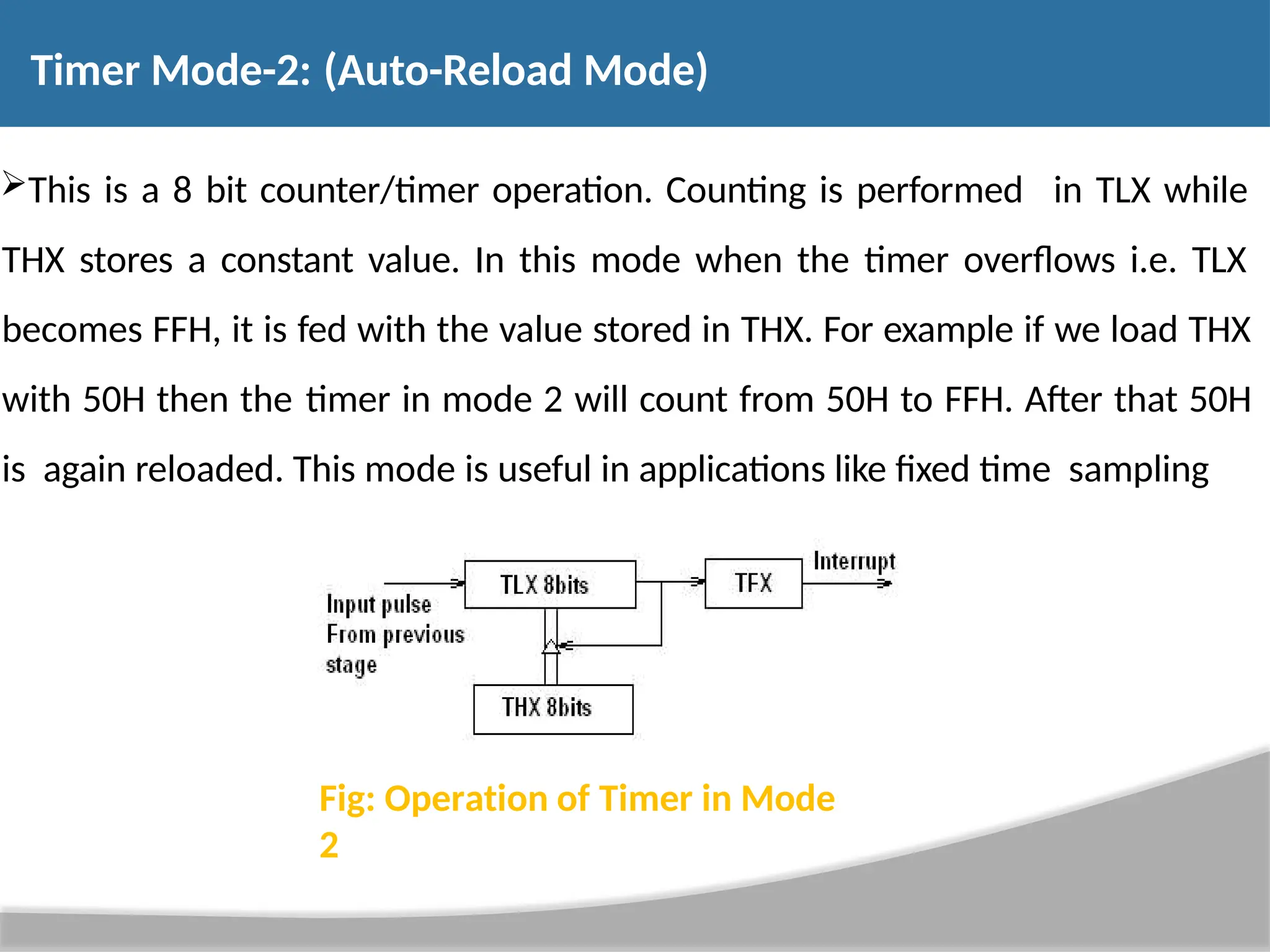
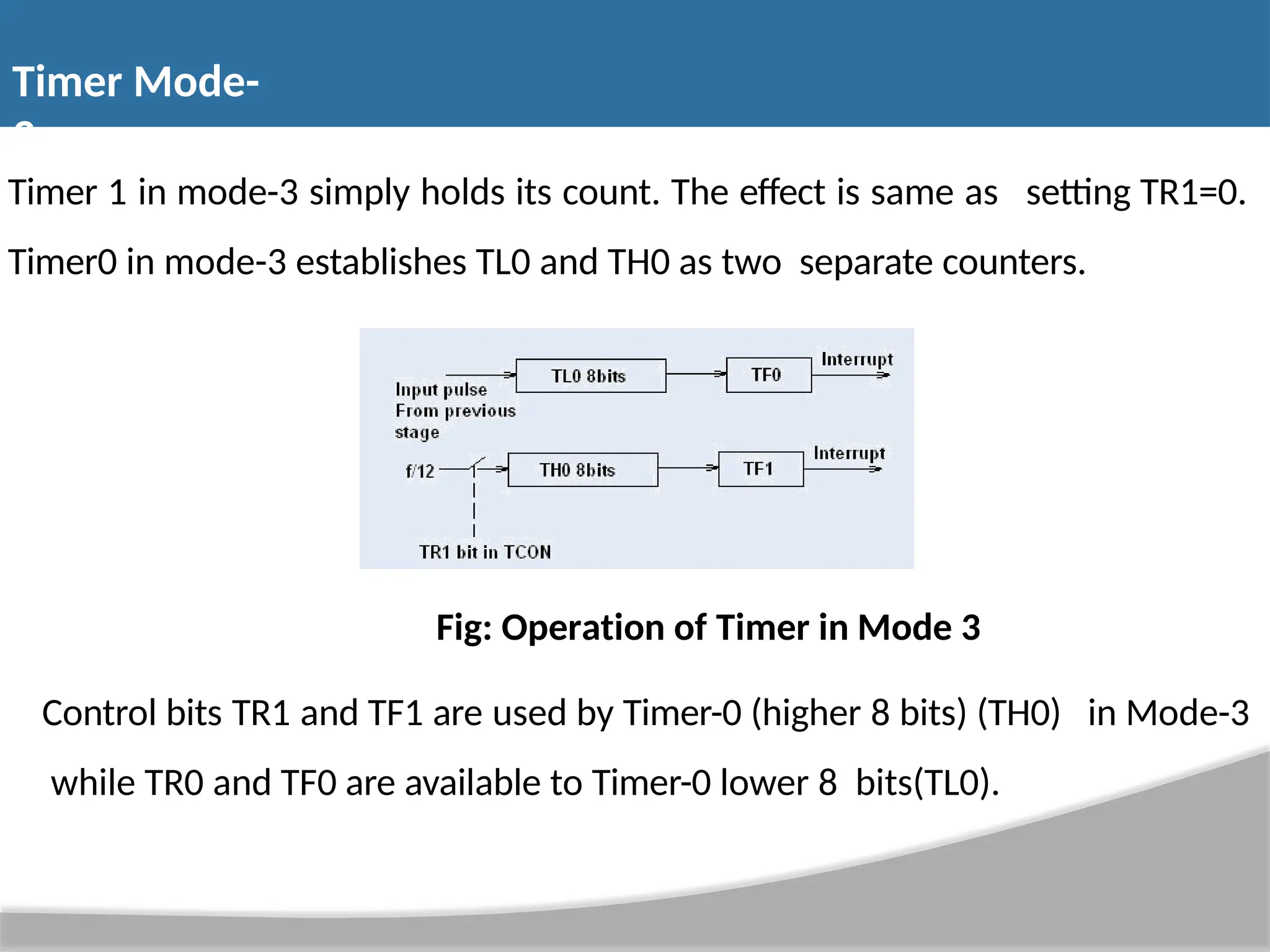
Introduction to processor: 2 •A processor is the logic circuitry that responds to and processes the basic instructions that drives a computer. • The term processor has generally replaced the term central processing unit . The processor in a personal computer or embedded in small devices is often called a microprocessor. • The processor (CPU, for Central Processing Unit) is the computer's brain. It allows the processing of numeric data, meaning information entered in binary form, and the execution of instructions stored in memory.
3.
Evolution of Microprocessor: 3 •A microprocessor is used as the CPU in a microcomputer. There are now many different microprocessors available. • Microprocessor is a program-controlled device, which fetches the instructions from memory, decodes and executes the instructions. Most Micro Processor are single- chip devices. • Microprocessor is a backbone of computer system. which is called CPU • Microprocessor speed depends on the processing speed depends on DATA BUS WIDTH. • A common way of categorizing microprocessors is by the no. of bits that their ALU can Work with at a time
4.
The addressbus is unidirectional because the address information is always given by the Micro Processor to address a memory location of an input / output devices. The data bus is Bi-directional because the same bus is used for transfer of data between Micro Processor and memory or input / output devices in both the direction. It has limitations on the size of data. Most Microprocessor does not support floating-point operations. Microprocessor contain ROM chip because it contain instructions to execute data. Storage capacity is limited. It has a volatile memory. In secondary storage device the storage capacity is larger. It is a nonvolatile memory. 4 Evolution of Microprocessor:
5.
Primary devicesare: RAM (Read / Write memory, High Speed, Volatile Memory) / ROM (Read only memory, Low Speed, Non Volatile Memory) Compiler: Compiler is used to translate the high-level language program into machine code at a time. It doesn’t require special instruction to store in a memory, it stores automatically. The Execution time is less compared to Interpreter 5 Evolution of Microprocessor:
6.
RISC (Reduced InstructionSet Computer): • RISC stands for Reduced Instruction Set Computer. To execute each instruction, if there is separate • electronic circuitry in the control unit, which produces all the necessary signals, this approach of the design of the control section of the processor is called RISC design. It is also called hardwired approach. Examples of RISC processors: • IBM RS6000, MC88100 • DEC’s Alpha 21064, 21164 and 21264 processors 6 Evolution of Microprocessor:
7.
Features of RISCProcessors: 7 The standard features of RISC processors are listed below: RISC processors use a small and limited number of instructions. RISC machines mostly uses hardwired control unit. RISC processors consume less power and performance. are having high Each instruction is very simple and consistent. RISC processors uses simple addressing modes. RISC instruction is of uniform fixed length
8.
CISC (Complex InstructionSet Computer): 8 CISC stands for Complex Instruction Set Computer. If the control unit contains a number of microelectronic circuitry to generate a set of control signals and each micro circuitry is activated by a micro code, this design approach is called CISC design. Examples of CISC processors are: Intel 386, 486, Pentium, Pentium Pro, Pentium II, Pentium III Motorola’s 68000, 68020, 68040, etc. Features of RISC Processors:
9.
Features of CISCProcessors: 9 CISC chips have a large amount of different and complex instructions. CISC machines generally make use of complex addressing modes. Different machine programs can be executed on CISC machine. CISC machines uses micro-program control unit. CISC processors are having limited number of registers
8086 Microprocessoris divided into two EU(Execution Unit) and BIU (Bus Interface Unit). 11 functional units, i.e., EU (Execution Unit): Execution unit gives instructions to BIU stating from where to fetch the data and then decode and execute those instructions. Its function is to control operations on data using the instruction decoder & ALU. EU has no direct connection with system buses as shown in the above figure, it performs operations over data through BIU. 8086 Architecture :
12.
• BIU(Bus InterfaceUnit): BIU takes care of all data and addresses transfers on the buses for the EU like sending addresses, fetching instructions from the memory, reading data from the ports and the memory as well as writing data to the ports and the memory. EU has no direction connection with System Buses so this is possible with the BIU. EU and BIU are connected with the Internal Bus. • Instruction queue: BIU contains the instruction queue. BIU gets up to 6 bytes of next instructions and stores them in the instruction queue. When EU executes instructions and is ready for its next instruction, then it simply reads the instruction from this instruction queue resulting in increased execution speed. 12 8086 Architecture :
13.
• Segment register: BIU has 4 segment buses, i.e. CS, DS, SS& ES. It holds the addresses of instructions and data in memory, which are used by the processor to access memory locations. It also contains 1 pointer register IP, which holds the address of the next instruction to executed by the EU. 13 8086 Architecture :
14.
AX & DXregisters: In 8 bit multiplication, one of the operands must be in AL. The other operand can be a byte in memory location or in another 8 bit register. The resulting 16 bit product is stored in AX, with AH storing the MS byte. In 16 bit multiplication, one of the operands must be in AX. The other operand can be a word in memory location or in another 16 bit register. The resulting 32 bit product is stored in DX and AX, with DX storing the MS word and AX storing the LS word. 14 Special functions of general purpose register
15.
Special functions ofgeneral purpose register 15 BX register : In instructions where we need to specify in a general purpose register the 16 bit effective address of a memory location, the register BX is used (register indirect). CX register : In Loop Instructions, CX register will be always used as the implied counter. In I/O instructions, the 8086 receives into or sends out data from AX or AL depending as a word or byte operation.
16.
• Segment register: BIU has 4 segment buses, i.e. CS, DS, SS& ES. It 16 holds the addresses of instructions and data in memory, which are used by the processor to access memory locations. It also contains 1 pointer register IP, which holds the address of the next instruction to executed by the EU. Segment register:
17.
Flag Registercontains a group of status bits called flags that indicate the status of the CPU or the result of arithmetic operations. There are two types of flags: The status flags which reflect the result of executing an instruction. The programmer cannot set/reset these flags directly. The control flags enable or disable certain CPU operations. The programmer can set/reset these bits to control the CPU's operation. 17 Flag Register and Functions of 8086 Flags
18.
• Nine individualbits of the status register are used as control flags (3 of them) and status flags (6 of them).The remaining 7 are not used. • A flag can only take on the values 0 and 1. We say a flag is set if it has the value 1.The status flags are used to record specific characteristics of arithmetic and of logical instructions. 18 Flag Register and Functions of 8086 Flags
• Control Flags:There are three control flags • The Direction Flag (D): Affects the direction of moving data blocks by such instructions as MOVS, CMPS and SCAS. The flag values are 0 = up and 1 = down and can be set/reset by the STD (set D) and CLD (clear D) instructions. • The Interrupt Flag (I): Dictates whether or not system interrupts can occur. Interrupts are actions initiated by hardware block such as input devices that will interrupt the normal execution of programs. The flag values are 0 = disable interrupts or 1 = enable interrupts and can be manipulated by the CLI (clear I) and STI (set I) instructions. 20 Flag Register and Functions of 8086 Flags
21.
• The TrapFlag (T): Determines whether or not the CPU is halted after the execution of each instruction. When this flag is set (i.e. = 1), the programmer can single step through his program to debug any errors. When this flag = 0 this feature is off. This flag can be set by the INT 3 instruction. • Status Flags: There are six status flags • The Carry Flag (C): This flag is set when the result of an unsigned arithmetic operation is too large to fit in the destination register. This happens when there is an end carry in an addition operation or there an end borrows in a subtraction operation. A value of 1 = carry and 0 = no carry. 21 Flag Register and Functions of 8086 Flags
22.
• The OverflowFlag (O): This flag is set when the result of a signed arithmetic operation is too large to fit in the destination register (i.e. when an overflow occurs). Overflow can occur when adding two numbers with the same sign (i.e. both positive or both negative). A value of 1 = overflow and 0 = no overflow. • The Sign Flag (S): This flag is set when the result of an arithmetic or logic operation is negative. This flag is a copy of the MSB of the result (i.e. the sign bit). A value of 1 means negative and 0 = positive. 22 Flag Register and Functions of 8086 Flags
23.
• The ZeroFlag (Z): This flag is set when the result of an arithmetic or logic operation is equal to zero. A value of 1 means the result is zero and a value of 0 means the result is not zero. • The Auxiliary Carry Flag (A): This flag is set when an operation causes a carry from bit 3 to bit 4 (or a borrow from bit 4 to bit 3) of an operand. A value of 1 = carry and 0 = no carry. • The Parity Flag (P): This flags reflects the number of 1s in the result of an operation. If the number of 1s is even its value = 1 and if the number of 1s is odd then its value = 0. 23 Flag Register and Functions of 8086 Flags
24.
• Addressing modeindicates a way of locating data or operands. Depending up on the data type used in the instruction and the memory addressing modes, any instruction may belong to one or more addressing modes or same instruction may not belong to any of the addressing modes. • The addressing mode describes the types of operands and the way they are 24 accessed for executing an instruction. According to the execution, the instructions may be categorized as Sequential control flow instructions and Control transfer instructions. flow of instruction Addressing Modes of 8086
25.
• Sequential controlflow instructions are the instructions which after execution, transfer control to the next instruction appearing immediately after it (in the sequence) in the program. For example the arithmetic, logic, data transfer and processor control instructions are Sequential control flow instructions. • The control transfer instructions on the other hand transfer control to some predefined address or the address somehow specified in the instruction, after their execution. For example INT, CALL, RET & JUMP instructions fall under this category. 25 Addressing Modes of 8086
26.
The addressingmodes for Sequential and control flow instructions are explained as follows. Immediate addressing mode: In this type of addressing, immediate data is a part of instruction, and appears in the form of successive byte or bytes. 26 Example: MOV AX, 0005H. In the above example, 0005H is the immediate data. The immediate may be 8- bit or 16-bit in size. data Addressing Modes of 8086
27.
Direct addressing mode: •In the direct addressing mode, a 16-bit memory address (offset) directly specified in the instruction as a part of it. Example: MOV AX, [5000H]. Register addressing mode: 27 • In the register addressing mode, the data is stored in a register and it is referred using the particular register. All the registers, except IP, used in this mode. may be Example: MOV BX, AX Addressing Modes of 8086
28.
Register indirect addressingmode: • Sometimes, the address of the memory location which contains data or operands is determined in an indirect way, using the offset registers. The mode of addressing is known as register indirect mode. • In this addressing mode, the offset address of data is in either BX or SI or DI Register. The default segment is either DS or ES. E• xample: MOV AX, [BX]. 28 Addressing Modes of 8086
29.
Indexed addressing mode: •In this addressing mode, offset of the operand is stored one of the index registers. DS & ES are the default segments for index registers SI & DI respectively. Example: MOV AX, [SI] • Here, data is available at an offset address stored in SI in DS. 29 Addressing Modes of 8086
30.
Register relative addressingmode: • In this addressing mode, the data is available at an effective address formed by adding an 8-bit or 16-bit displacement with the content of any one of the register BX, BP, SI & DI in the default (either in DS & ES) segment. 30 Example: MOV AX, 50H [BX] Addressing Modes of 8086
31.
• 31 • Based indexed addressingmode: • The effective address of data is formed in this addressing mode, by adding content of a base register (any one of BX or BP) to the content of an index register (any one of SI or DI). The default segment register may be ES or DS. Example: MOV AX, [BX][SI] Relative based indexed: • The effective address is formed by adding an 8 or 16-bit displacement with the sum of contents of any of the base registers (BX or BP) and any one of the index registers, in a default segment. Example: MOV AX, 50H [BX] [SI] • Addressing Modes of 8086
32.
• Addressing Modesfor control transfer instructions: • Intersegment – Intersegment direct – Intersegment indirect • Intrasegment – Intrasegment direct – Intrasegment indirect 32 Addressing Modes of 8086
33.
• Intersegment direct: In this mode, the address to which the control is to be transferred is in a different segment. This addressing mode provides a means of branching from one code segment to another code segment. Here, the CS and IP of the destination address are specified directly in the instruction. Example: JMP 5000H: 2000H; • Jump to effective address 2000H in segment 5000H. 33 Addressing Modes of 8086
34.
Intersegment indirect: Inthis mode, the address to which the control is to be transferred lies in a different segment and it is passed to the instruction indirectly, i.e. contents of a memory block containing four bytes, i.e. IP(LSB), IP(MSB), CS(LSB) and CS(MSB) sequentially. The starting address of the memory block may be referred using any of the addressing modes, except immediate mode. Example: JMP [2000H]. 34 Jump to an address in the other segment specified at effective 2000H in DS. address Addressing Modes of 8086
35.
• Intrasegment directmode: In this mode, the address to which the control is to be transferred lies in the same segment in which the control transfers instruction lies and appears directly in the instruction as an immediate displacement value. In this addressing mode, the displacement is computed relative to the content of the instruction pointer. 35 Addressing Modes of 8086
36.
• The effectiveaddress to which the control will be transferred is given by 36 the sum of 8 or 16 bit displacement and current content of jump instruction, if the signed displacement (d) is of 8- IP . In case of bits (i.e. - 128<d<+127), it as short jump and if it is of 16 bits (i.e. - 32768<d<+32767), it is termed as long jump. Example: JMP SHORT LABEL. Addressing Modes of 8086
37.
• Intrasegment indirectmode: • In this mode, the displacement to which the control is to be transferred is in the same segment in which the control transfer instruction lies, but it is passed to the instruction directly. Here, the branch address is found as the content of a register or a memory location. • This addressing mode may be used in unconditional branch instructions. • Example: JMP [BX]; Jump to effective address stored in BX. 37 Addressing Modes of 8086
38.
INSTRUCTION SET OF8086 38 • The Instruction set of 8086 microprocessor is classified into 7 Types, they are:- • Data transfer instructions • Arithmetic& logical instructions • Program control transfer instructions • Machine Control Instructions • Shift / rotate instructions • Flag manipulation instructions • String instructions
39.
• Data transferinstruction, as the name suggests is for the transfer of data from memory to internal register, from internal register to memory, from one register to another register, from input port to internal register, from internal register to output port etc MOV instruction • It is a general purpose instruction to transfer byte or word from register to register, memory to register, register to memory or with immediate addressing. 39 Data Transfer instructions
40.
General Form: • MOVdestination, source • Here the source and destination needs to be of the same size, that is both 8 bit or both 16 bit. • MOV instruction does not affect any flags. Example:- 40 • • MOV BX, 00F2H; load the immediate number 00F2H in BX register • MOV CL, [2000H] ;Copy the 8 bit content of the memory location, at a displacement of2000H from data segment base to the CL register Data Transfer instructions
41.
•MOV [589H], BX;Copy the 16 bit content of BX register on to the memory location, which at a displacement of 589H from the data segment base. • MOV DS, CX; Move the content of CX to DS PUSH instruction • The PUSH instruction decrements the stack pointer by two and copies the word from source to the location where stack pointer now points. Here the source must of word size data. Source can be a general purpose register, segment register or a memory location. 41 Data Transfer instructions
42.
The PUSH instructionfirst pushes the most significant byte to sp-1, then the least significant to the sp-2. Push instruction does not affect any flags. 42 Data Transfer instructions
43.
Example:- • PUSH CX 43 ;Decrements SP by 2, copy content of CX to the stack (figure shows execution of this instruction) ; Decrement SP by 2 and copy DS to stack • PUSH DS • POP instruction The POP instruction copies a word from the stack location pointed by the stack pointer to the destination. The destination can be a General purpose register, a segment register or a memory location. Here after the content is copied the stack pointer is automatically incremented by two. • The execution pattern is similar to that of the PUSH instruction. Example: • POP CX ; Copy a word from the top of the stack to CX and increment SP by 2. Data Transfer instructions
44.
Move 8 bitdata from 30F8H port Move 16 bit data from 30F8H port Copy contents of AL to 8 bit port 047H 44 • IN & OUT instructions • The IN instruction will copy data from a port to the accumulator. If 8 bit is read the data will go to AL and if 16 bit then to AX. Similarly OUT instruction is used to copy data from accumulator to an output port. • Both IN and OUT instructions can be done using direct and indirect addressing modes. Example: • IN AL, 0F8H; Copy a byte from the port 0F8H to AL • MOV DX, 30F8H;Copy port address in DX • IN AL, DX; • IN AX, DX; • OUT 047H, AL; • MOV DX, 30F8H;Copy port address in DX Data Transfer instructions
45.
XCHG instruction • TheXCHG instruction exchanges contents of the destination and source. Here destination and source can be register and register or register and memory location, but XCHG cannot interchange the value of 2 memory locations. General Format • XCHG Destination, Source Example: • XCHG BX, CX; exchange word in CX with the word in BX • XCHG AL, CL; exchange byte in CL with the byte in AL • XCHG AX, SUM[BX];here physical address, which is DS+SUM+[BX]. The content at physical address and the content of AX are interchanged. 45 Data Transfer instructions
46.
Mnemonic Meaning FormatOperation Flags affected ADD Addition ADD D,S (S)+(D) (D) carry (CF) ALL ADC Add with carry ADC D,S (S)+(D)+(CF) (D) carry (CF) ALL INC Increment by one INC D (D)+1 (D) ALL but CY AAA ASCII adjust for addition AAA If the sum is >9,AH is incremented by 1 AF,CF DAA Decimal adjust for addition DAA Adjust AL for decimal Packed BCD ALL 46 Arithmetic Instructions: ADD, ADC, INC, AAA, DAA
47.
Arithmetic Instructions–SUB, SBB,DEC, AAS, DAS, NEG 47 Mnemonic Meaning Format Operation Flags affected SUB Subtract SUB D,S (D) - (S) (D) Borrow (CF) All SBB Subtract with borrow SBB D,S (D) - (S) - (CF) (D) All DEC Decrement by one DEC D (D) - 1 (D) All but CF NEG Negate NEG D All DAS Decimal adjust for subtraction DAS Convert the result in AL to packed decimal format All AAS ASCII adjust for subtraction AAS (AL) difference (AH) dec by 1 if borrow CY,AC
AND instruction • Thisinstruction logically ANDs each bit of the source byte/word with the corresponding bit in the destination and stores the result in destination. The source can be an immediate number, register or memory location, register can be a register or memory location. • The CF and OF flags are both made zero, PF, ZF, SF are affected by the operation and AF is undefined. • General Format: • AND Destination, Source Example: 50 • AND BL, AL ;suppose BL=1000 0110 and AL = 1100 1010 then after the operation BL would be BL= 1000 0010. • AND CX, AX ;CX <= CX AND AX • AND CL, 08 ;CL<= CL AND (0000 1000) Logical Instructions
51.
OR instruction • Thisinstruction logically ORs each bit of the source byte/word with the corresponding bit in the destination and stores the result in destination. The source can be an immediate number, register or memory location, register can be a register or memory location. • The CF and OF flags are both made zero, PF, ZF, SF are affected by the operation and AF is undefined. • General Format: • OR Destination, Source 51 Logical Instructions
52.
Example: • OR BL,AL; suppose BL=1000 0110 and AL = 1100 1010 then after the operation BL would be BL= 1100 1110. • OR CX, AX;CX <= CX AND AX • OR CL, 08;CL<= CL AND (0000 1000) NOT instruction • The NOT instruction complements (inverts) the contents of an operand register or a memory location, bit by bit. The examples are as follows: Example: • NOT AX (BEFORE AX= (1011)2= (B) 16 AFTER EXECUTION AX= (0100)2= (4)16). • NOT [5000H] 52 Logical Instructions
53.
XOR instruction • TheXOR operation is again carried out in a similar way to the AND and OR operation. The constraints on the operands are also similar. The XOR operation gives a high output, when the 2 input bits are dissimilar. Otherwise, the output is zero. The example instructions are as follows: Example: • XOR AX,0098H • XOR AX,BX • XOR AX,[5000H] 53 Logical Instructions
54.
Shift / RotateInstructions • Shift instructions move the binary data to the left or right by them within the register or memory location. They also can multiplication of powers of 2+n and division of powers of 2-n. 54 shifting perform • There are two type of shifts logical shifting and arithmetic shifting, later is used with signed numbers while former with unsigned. Logical Instructions
55.
SHL/SAL instruction • Boththe instruction shifts each bit to left, and places the MSB in CF and LSB is made 0. The destination can be of byte size or of word size, also it can be a register or a memory location. Number of shifts is indicated by the count. • All flags are affected. General Format: • SAL/SHL destination, count 55 Logical Instructions
56.
SHR instruction 56 • Thisinstruction shifts each bit in the specified destination to the right and 0 is stored in the MSB position. The LSB is shifted into the carry flag. The destination can be of byte size or of word size, also it can be a register or a memory location. Number of shifts is indicated by the count. • All flags are affected • General Format: SHR destination, count Logical Instructions
57.
String - abyte or word array located in memory. Operations that can be performed with string instructions: • copy a string into another string • search a string for a particular byte or word • store characters in a string • compare strings of characters alphanumerically 57 String Instruction Basics
58.
Source DS:SI,Destination ES:DI – You must ensure DS and ES are correct – You must ensure SI and DI are offsets into DS and ES respectively Direction Flag (0 = Up, 1 = Down) – CLD - Increment addresses (left to right) – STD - Decrement addresses (right to left) 58 String Instruction Basics
59.
String Control Instructions 59 1) MOVS/MOVSB/ MOVSW Dest string name, src string name This instruction moves data byte or word from location in DS to location in ES. 2) REP / REPE / REPZ / REPNE / REPNZ Repeat string instructions until specified conditions exist. This is prefix a instruction. 3) CMPS / CMPSB / CMPSW Compare string bytes or string words.
60.
4)SCAS / SCASB/ SCASW Scan a string byte or string word. Compares byte in AL or word in AX. String address is to be loaded in DI. 5)STOS / STOSB / STOSW Store byte or word in a string. Copies a byte or word in AL or AX to memory location pointed by DI. 6)LODS / LODSB /LODSW Load a byte or word in AL or AX Copies byte or word from memory location pointed by SI into AL or AX register. 60 String Control Instructions
61.
5. Program ExecutionTransferInstructions 61 These instructions are similar to branching or looping instructions. These instructions include unconditional jump or loop instructions. Classification: •Unconditional transfer instructions •Conditional transfer instructions •Iteration control instructions •Interrupt instructions
62.
Unconditional transfer instructions CALL: Call a procedure, save return address on stack RET: Return from procedure to the main program. JMP: Goto specified address to get next instruction CALL instruction: The CALL instruction is used to transfer execution of program to a subprogram or procedure. 62 5. Program Execution TransferInstructions
63.
CALL instruction Nearcall 1.Direct Near CALL: The destination address is specified in the instruction itself. 2.Indirect Near CALL: The destination address is specified in any 63 16-bit register, except IP. Far call 1.DirectFar CALL: The destination address is specified in the instruction itself. It will be in different Code Segment. 2. Indirect Far CALL: The destination address is specified in two word memory locations pointed by a register. 5. Program Execution TransferInstructions
64.
JMP instruction The processorjumps to the specified location rather than the instruction after the JMP instruction. Intra segment jump Inter segment jump RET RET instruction will return execution from a procedure to the next instruction after the CALL instruction in the calling program. 64 5. Program Execution TransferInstructions
65.
Conditional TransferInstructions • JA/JNBE:Jump if above / jump if not below or equal • JAE/JNB: Jump if above /jump if not below • JBE/JNA: Jump if below or equal/ Jump if not above • JC: jump if carry flag CF=1 • JE/JZ: jump if equal/jump if zero flag ZF=1 • JG/JNLE: Jump if greater/ jump if not less than or equal. 65 5. Program Execution TransferInstructions
66.
Conditional Transfer Instructions •JGE/JNL: jump if greater than or equal/ jump if not less than • JL/JNGE: jump if less than/ jump if not greater than or equal • JLE/JNG: jump if less than or equal/ jump if not greater than • JNC: jump if no carry (CF=0). • JNE/JNZ: jump if not equal/ jump if not zero(ZF=0) 66 5. Program Execution TransferInstructions
67.
Conditional Transfer Instructions •JNO: jump if no overflow(OF=0) • JNP/JPO: jump if not parity/ jump if parity odd(PF=0) • JNS: jump if not sign(SF=0) • JO: jump if overflow flag(OF=1) • JP/JPE: jump if parity/jump if parity even(PF=1) • JS: jump if sign(SF=1). 67 5. Program Execution TransferInstructions
68.
Iteration Control Instructions These instructions are used to execute a series of instructions for certain number of times. LOOP: Loop through a sequence of instructions until CX=0. 68 instructions while LOOPE/LOOPZ : Loop through a sequence of ZF=1 and instructions CX = 0. LOOPNE/LOOPNZ : Loop through a sequence of instructions while ZF=0 and CX =0. JCXZ : jump to specified address if CX=0. 5. Program Execution Transfer Instructions
69.
Interrupt Instructions 69 Two typesof interrupt instructions: Hardware Interrupts (External Interrupts) Software Interrupts (Internal Interrupts and Instructions) Hardware Interrupts: • INTR is a maskable hardware interrupt. • NMI is a non-maskable interrupt.
70.
Software Interrupts • INT: Interrupt program execution, call service procedure • INTO : Interrupt program execution if OF=1 • IRET: Return from interrupt service procedure to main program. 70 Interrupt Instructions
71.
ENTER : enterprocedure. LEAVE: Leaveprocedure. BOUND: Check if effective address within specified array bounds. 71 High Level Language Interface Instructions
72.
Processor Control Instructions 72 I. Flagset/clear instructions STC: Set carry flag CF to 1 CLC: Clear carry flag CF to 0 CMC: Complement the state of the carry flag CF STD: Set direction flag DF to 1 (decrement string pointers) CLD: Clear direction flag DF to 0 STI: Set interrupt enable flag to 1(enable INTR input) CLI: Clear interrupt enable Flag to 0 (disable INTR input)
73.
II. External Hardwaresynchronizationinstructions HLT: Halt (do nothing) until interrupt or reset. WAIT: Wait (Do nothing) until signal on the test pin islow. ESC: Escape to external coprocessor such as 8087 or 8089. LOCK: An instruction prefix. Prevents another processor from taking the bus while the adjacent instruction executes. NOP: No operation. This instruction simply takes up three clock cycles and does no processing. 73 Processor Control Instructions
74.
Assembler Directives 74 ASSUME DB DD DQ DT DW - - - - - Defined Byte. Defined Double Word Defined Quad Word Define Ten Bytes Define Word
75.
ASSUME Directive- TheASSUME directive is used to tell the assembler that the name of the logical segment should be used for a specified segment. The 8086 works directly with only 4 physical segments: a Code segment, a data segment, a stack segment, and an extra segment. Example: ASUME CS:CODE ;This tells the assembler that the logical segment named CODE contains the instruction statements for the program and should be treated as a code segment. ASSUME DS:DATA ;This tells the assembler that for any instruction which refers to a data in the data segment, data will found in the logical segment DATA. 75 Assembler Directives
76.
DB -DB directive is used to declare a byte- type variable or to in memory location. 76 store a byte Example: 1. PRICE DB 49h, 98h, 29h ; Declare an array of 3 bytes, PRICE and initialize. named as 2. NAME DB ‘ABCDEF’ ;Declare an array of 6 bytes and initialize with ASCII code for letters 3. TEMP DB 100 DUP(?) ;Set 100 bytes of storage in memory and give it the name as TEMP, but leave the 100 bytes uninitialized. Program instructions will load values into these locations. Assembler Directives
77.
DW 77 -The DWdirective is used to define a variable of type word or to reserve storage location of type word in memory. Example: • MULTIPLIER DW 437Ah ; this declares a variable of type word and named it as MULTIPLIER. This variable is initialized with the value 437Ah when it is loaded into memory to run. Assembler Directives
78.
END -END directive is placed after the last statement of a program to tell the assembler that this is the end of the program module. The assembler will ignore any statement after an END directive. ENDP - ENDPdirective is used along with the name of the procedure to indicate the end of a procedure to the assembler Example: • SQUARE_NUM PROCE ; It start the procedure, Some steps to find the square root of a number • SQUARE_NUM ENDP ;Hear it is the End for the procedure 78 Assembler Directives
79.
END ENDP ENDS EQU EVEN EXTRN 79 - End Program - End Procedure - End Segment - Equate - Align on Even Memory Address - Assembler Directives
80.
ENDS -This ENDS directive is used with name of the segment to indicate the end of that logic segment. Example: CODE SEGMENT ;Hear it Start the logic segment containing code ; CODE ENDS ;End of segment named as CODE GLOBAL - Can be used in place of a PUBLIC directive or in place of an EXTRN directive. 80 Assembler Directives
81.
GROUP -Used to tell the assembler to group the logical statements named after the directive into one logical group segment, allowing the contents of all the segments to be accessed from the same group segment base. INCLUDE - Used to tell the assembler to insert a block of source code from the named file into the current source module. LABEL- Used to give a name to the current value in the location counter. NAME- Used to give a specific name to each assembly module when programs consisting of several modules are written. E.g.: NAME PC_BOARD 84 Assembler Directives
82.
OFFSET- Usedto determine the offset or displacement of a named item or procedure from the start of the segment which contains it. 82 dat a E.g.: MOV BX, OFFSET PRICES ORG- The location counter is set to 0000 when the assembler starts reading a segment. The ORG directive allows setting a desired value at any point in the program. E.g.: ORG 2000H Assembler Directives
83.
PUBLIC- Usedto tell the assembler that a specified name or label accessed from other modules. 83 will be SEGMENT- Used to indicate the start of a logical segment. E.g.: CODE SEGMENT indicates to the assembler the start of a segment called CODE logical SHORT- Used to tell the assembler that only a 1 byte displacement is needed to code a jump instruction. E.g.: JMP SHORT NEARBY_LABEL TYPE - Used to tell the assembler to determine the type of specified variable. Assembler Directives
84.
Write an assemblylanguage program for addition of two 8- bit numbers using 8086 microprocessors. 84 DATA SEGMENT A1 DB 50H A2 DB 51H RES DB ? DATA ENDS CODE SEGMENT ASSUME CS: CODE, DS:DATA START : MOV AX,DATA MOV DS,AX MOV AL,A1 MOV BL,A2 ADD AL,BL MOV RES,AL MOV AX,4C00H INT 21H CODE ENDS END START
85.
Write an assemblylanguage program to find the factorial of given number using 8086 microprocessors. 85 DATA SEGMENT FIRST DW 03H SEC DW 01H DATA ENDS CODE SEGMENT ASSUME CS:CODE,DS:DATA START : MOV AX,DATA MOV DS,AX MOV AX,SEC MOV CX,FIRST L1: MUL CX DEC CX JCXZ L2 JMP L1 L2: INT 3H CODE ENDS END START
86.
Write an assemblylanguage program to find the sum of squares using 8086 microprocessors. 86 DATA SEGMENT NUM DW 5H RES DW ? DATA ENDS CODE SEGMENT ASSUME CS: CODE, DS: DATA START: MOV AX,DATA MOV DS,AX MOV CX,NUM MOV BX,00 L1: MOV AX,CX MUL CX ADD BX,AX DEC CX JNZ L1 MOV RES,BX INT 3H CODE ENDS END START
87.
Procedures: • While writingprograms, it may be the case that a particular sequence of instructions is used several times. To avoid writing the sequence of instructions again and again in the program, the same sequence can be written as a separate subprogram called a procedure. Defining Procedures: 87 • Assembler provides PROC and ENDP directives in order to define procedures. The directive PROC indicates beginning of a procedure. Its general form is: Procedure_name PROC [NEAR|FAR] Procedures and Macros
88.
Passing parameters toand from procedures: The data values or addresses passed between procedures and main program are called parameters. There are four ways of passing parameters: Passing parameters in registers Passing parameters in dedicated memory locations Passing parameters with pointers passed in registers Passing parameters using the stack 88 Procedures and Macros
89.
MACROS: When therepeated group of instruction is too short or not suitable to be implemented as a procedure, we use a MACRO. A macro is a group of instructions to which a name is given. Each time a macro is called in a program, the assembler will replace the macro name with the group of instructions. Defining MACROS: Before using macros, we have to define them. MACRO directive informs the assembler the beginning of a macro. The general form is: 130 Macro_name MACRO argument1, argument2, …Arguments are optional. ENDM informs the assembler the end of the macro. Its general form is : ENDM Procedures and Macros
90.
Procedures Macros Accessed byCALL and RET mechanism during program execution Accessed by name given to macro when defined during assembly Machine code for instructions only put in memory once Machine code generated for instructions each time called Parameters are passed in registers, memory locations or stack Parameters passed as part of statement which calls macro Procedures uses stack Macro does not utilize stack A procedure can be defined anywhere in program using the directives PROC and ENDP A macro can be defined anywhere in program using the directives MACRO and ENDM Procedures takes huge memory for CALL(3 bytes each time CALL is used) instruction Length of code is very huge if macro’s are called for more number of times 90 Procedures and Macros
In aminimum mode 8086 system, the microprocessor 8086 is operated in minimum mode by strapping its MN/MX pin to logic 1. In this mode, all the control signals are given out by the microprocessor chip itself. There is a single microprocessor in the minimum mode system. The remaining components in the system are latches, transceivers, clock generator, memory and I/O devices. Some type of chip selection logic may be required for selecting memory or I/O devices, depending upon the address map of the system. Latches are generally buffered output D-type flip-flops like 74LS373 or 8282. They are used for separating the valid address from the multiplexed address/data signals and are controlled by the ALE signal generated by 8086. 92 Minimum mode operation in 8086:
93.
Transceivers arethe bidirectional buffers and sometimes they are called as data amplifiers. They are required to separate the valid data from the time multiplexed address/data signals. They are controlled by two signals namely, DEN and DT/R. The DEN signal indicates the direction of data, i.e. from or to the processor. The system contains memory for the monitor and users program storage. Usually, EPROM is used for monitor storage, while RAM for users program storage. A system may contain I/O devices. 93 Minimum mode operation in 8086:
94.
In the maximummode, the 8086 is operated by strapping the MN/MX pin to ground. In this mode, the processor derives the status signal S2, S1, S0. Another chip called bus controller derives the control signal using this status information. In the maximum mode, there may be more than one 94 microprocessor in the system configuration. The components in the system are same as in the minimum mode system. The basic function of the bus controller chip IC8288 is to derive contro l signals like RD and WR (for memory and I/O devices), DEN, DT/R, ALE etc. using the information by the processor on the status lines. The bus controller chip has input lines S2, S1, S0 and CLK. These inputs to 8288 are driven by CPU. Maximum mode operation in 8086:
IOWC 140 • It derivesthe outputs ALE, DEN, DT/R, MRDC, MWTC, AMWC, IORC, and AIOWC. The AEN, IOB and CEN pins are especially useful for multiprocessor systems. • AEN and IOB are generally grounded. CEN pin is usually tied to +5V. The significance of the MCE/PDEN output depends upon the status of the IOB pin. • If IOB is grounded, it acts as master cascade enable to control cascade 8259A, else it acts as peripheral data enable used in the multiple bus configurations. Maximum mode operation in 8086:
97.
• INTA pinused to issue two interrupt acknowledge pulses to the interrupt 140 controller or to an interrupting device. • IORC, IOWC are I/O read command respectively. and I/O write command signals • These signals enable an IO interface to read or write the data from or to the address port. • The MRDC, MWTC are memory read command and memory write command signals respectively and may be used as memory read or write signals. Maximum mode operation in 8086:
98.
• The MRDC,MWTC are memory read command and memory write write 98 command signals respectively and may be used as memory read or signals. • All these command signals instructs the memory to accept or send from or to the bus. dat a • For both of these write command signals, the advanced signals namely AIOWC and AMWTC are available. • Here the only difference between in timing diagram between minimum mode and maximum mode is the status signals used and the available control and advanced command signals. Maximum mode operation in 8086:
99.
• R0, S1,S2 are set at the beginning of bus cycle.8288 bus controller will output a pulse as on the ALE and apply a required signal to its DT / R pin during T1. • In T2, 8288 will set DEN=1 thus enabling transceivers, and for an input it will activate MRDC or IORC. These signals are activated until T4. For an output, the AMWC or AIOWC is activated from T2 to T4 and MWTC or IOWC is activated from T3 to T4. 99 Maximum mode operation in 8086:
Assembly Language Programming 105 The assembly developedby programming language is a low-level language which is using mnemonics. The microcontroller or microprocessor can understand only the binary language like 0’s or 1’s therefore the assembler convert the assembly language to binary language and store it the memory to perform the tasks. Before writing the program the embedded designers must have sufficient knowledge on particular hardware of the controller or processor, so first we required to know hardware of 8086 processor. Machine Language: Set of fundamental instructions the machine can execute Expressed as a pattern of 1’s and 0’s
106.
Assembly Language Programming 106 AssemblyLanguage: Alphanumeric equivalent of machine language Mnemonics more human- oriented than 1’s and 0’s Assembler: Computer program that transliterates (one-to-one mapping) assembly to machine language Computer’s native language is machine/assembly language
107.
Why Assembly LanguageProgramming 107 • Faster and shorter programs: Compilers do not always generate optimum code. • Instruction set knowledge is important for machine designers. • Compiler writers must be familiar with details of machine language. • Small controllers embedded in many products • Have specialized functions, • Rely so heavily on input/output functionality, • HLLs inappropriate for product development.
8086 assembly programminglanguage instructions 109 • Like we know instruction are the lines of a program that means an action for the computer to execute. In 8086, a normal instruction is made by an operation code and sometimes operands. Structure: Operation Code [Operand1 [, Operand2]] • Operations • The operation is usually logic or arithmetic, but we can also find some special operation like the Jump (JMP) operation.
110.
8086 assembly programminglanguage instructions 110 • Operands • Operands are the parameters of the operation in the instruction. They can be use in 3 way: • Immediate • This means a direct access of a variable that have been declared in the program. • Register • Here we use the content of a register to be a parameter. • Memory • Here we access to the content of a specific part of the memory using a pointer
111.
SYNTAX OF 8086/8088ASSEMBLY LANGUAGE 111 • The language is not case sensitive. • There may be only one statement per line. A statement may start in any column. • A statement is either an instruction, which the assembler translates into machine code, or an assembler directive (pseudo-op), which instructs the assembler to perform some specific task. • Syntax of a statement: {name} mnemonic {operand(s)} {; comment} • The curly brackets indicate those items that are not present or are optional in some statements.
112.
SYNTAX OF 8086/8088ASSEMBLY LANGUAGE 112 • The name field is used for instruction labels, procedure names, segment names, macro names, names of variables, and names of constants. • MASM 6.1 accepts identifier names up to 247 characters long. All characters are significant, whereas under MASM 5.1, names are significant to 31 characters only. Names may consist of letters, digits, and the following 6 special characters: ? . @ _ $ % .If a period is used; it must be the first character. Names may not begin with a digit. • Instruction mnemonics, directive mnemonics, register names, operator names and other words are reserved.
113.
Stac k 113 • A stackis a container of objects that are inserted and removed according to the last-in first-out (LIFO) principle. In the pushdown stacks only two operations are allowed: push the item into the stack, and pop the item out of the stack. • A stack is a container of objects that are inserted and removed according to the last-in first-out (LIFO) principle. In the pushdown stacks only two operations are allowed: push the item into the stack, and pop the item out of the stack. A stack is a limited access data structure - elements can be added and removed from the stack only at the top. push adds an item to the top of the stack, pop removes the item from the top.
114.
Stac k 114 • A helpfulanalogy is to think of a stack of books; you can remove only the top book, also you can add a new book on the top. A stack is a recursive data structure. Here is a structural definition of a Stack: • A stack is either empty or it consists of a top and the rest which is a stack;
115.
Applications 115 • The simplestapplication of a stack is to reverse a word. You push a given word to stack - letter by letter - and then pop letters from the stack. • Another application is an "undo" mechanism in text editors; this operation is accomplished by keeping all text changes in a stack. • Backtracking. This is a process when you need to access the most recent data element in a series of elements. Think of a labyrinth or maze - how do you find a way from an entrance to an exit? Once you reach a dead end, you must backtrack. But backtrack to where? to the previous choice point. Therefore, at each choice point you store on a stack all possible choices. Then backtracking simply means popping a next choice from the stack.
116.
Stack Data Structure 116 Stack isa linear data structure which follows a particular order in which the operations are performed. The order may be LIFO(Last In First Out) or FILO(First In Last Out). Mainly the following three basic operations are performed in the stack: • Push: Adds an item in the stack. If the stack is full, then it is said to be an Overflow condition. • Pop: Removes an item from the stack. The items are popped in the reversed order in which they are pushed. If the stack is empty, then it is said to be an Underflow condition.
• If thestack top points to a memory location 52050H, it means that the location 52050H is already occupied with the previously pushed data. The next 16 bit push operation will decrement the stack pointer by two, so that it will point to the new stack-top 5204EH and the decremented contents of SP will be 204EH. This location will now be occupied by the recently pushed data. • Thus for a selected value of SS, the maximum value of SP=FFFFH and the segment can have maximum of 64K locations. If the SP starts with an initial value of FFFFH, it will be decremented by two whenever a 16-bit data is pushed onto the stack. 118 Stack Structure
119.
• After successivepush operations, when the stack pointer contains 0000H, any attempt to further push the data to the stack will result in stack overflow. • After a procedure is called using the CALL instruction, the IP is incremented to the next instruction. Then the contents of IP, CS and flag register are pushed automatically to the stack. The control is then transferred to the specified address in the CALL instruction i.e. starting address of the procedure. Then the procedure is executed. 119 Stack Structure
120.
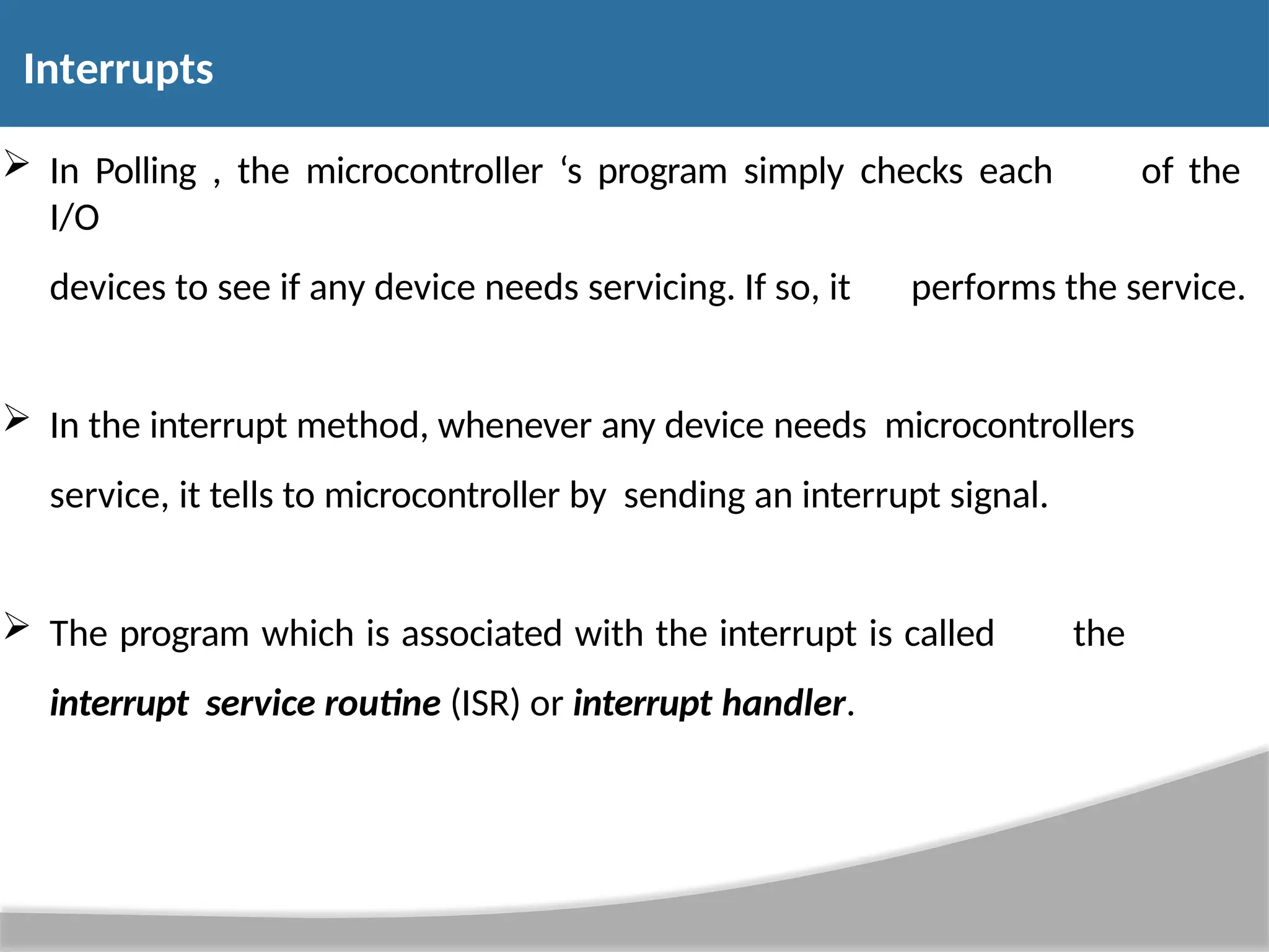
Interrupt s 120 Definition: The meaning of‘interrupts’ is to break the sequence of operation. While the CPU is executing a program, on ‘interrupt’ breaks the normal sequence of execution of instructions, diverts its execution to some other program called Interrupt Service Routine (ISR).After executing ISR , the control is transferred back again to the main program. Interrupt processing is an alternative to polling.
121.
Interrupt s 121 Need for Interrupt: Interruptsare particularly useful when interfacing I/O devices that provide or require data at relatively low data transfer rate. Interrupt is a mechanism that allows hardware or software to suspend normal execution on microprocessor in order to switch to interrupt service routine for hardware / software. Interrupt can also describe as asynchronous electrical signal that sent to a microprocessor in order to stop current execution and switch to the execution signaled (depends on priority). Whether an interrupt is prioritized or not depends on the interrupt flag register which controlled by priority / programmable interrupt
122.
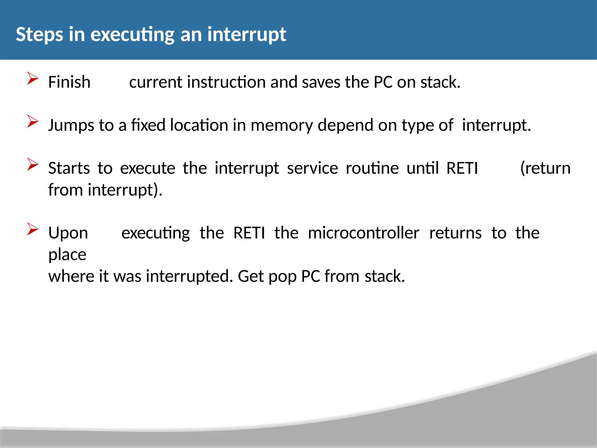
Interrupt Cycle of8086 122 • Interrupts in 8086 microprocessor. ... Whenever an interrupt occurs the processor completes the execution of the current instruction and starts the execution of an Interrupt Service Routine (ISR) or Interrupt Handler. ISR is a program that tells the processor what to do when the interrupt occurs. • In 8086 microprocessor following tasks are performed when microprocessor encounters an interrupt: • The value of flag register is pushed into the stack. It means that first the value of SP (Stack Pointer) is decremented by 2 then the value of flag register is pushed to the memory address of stack segment.
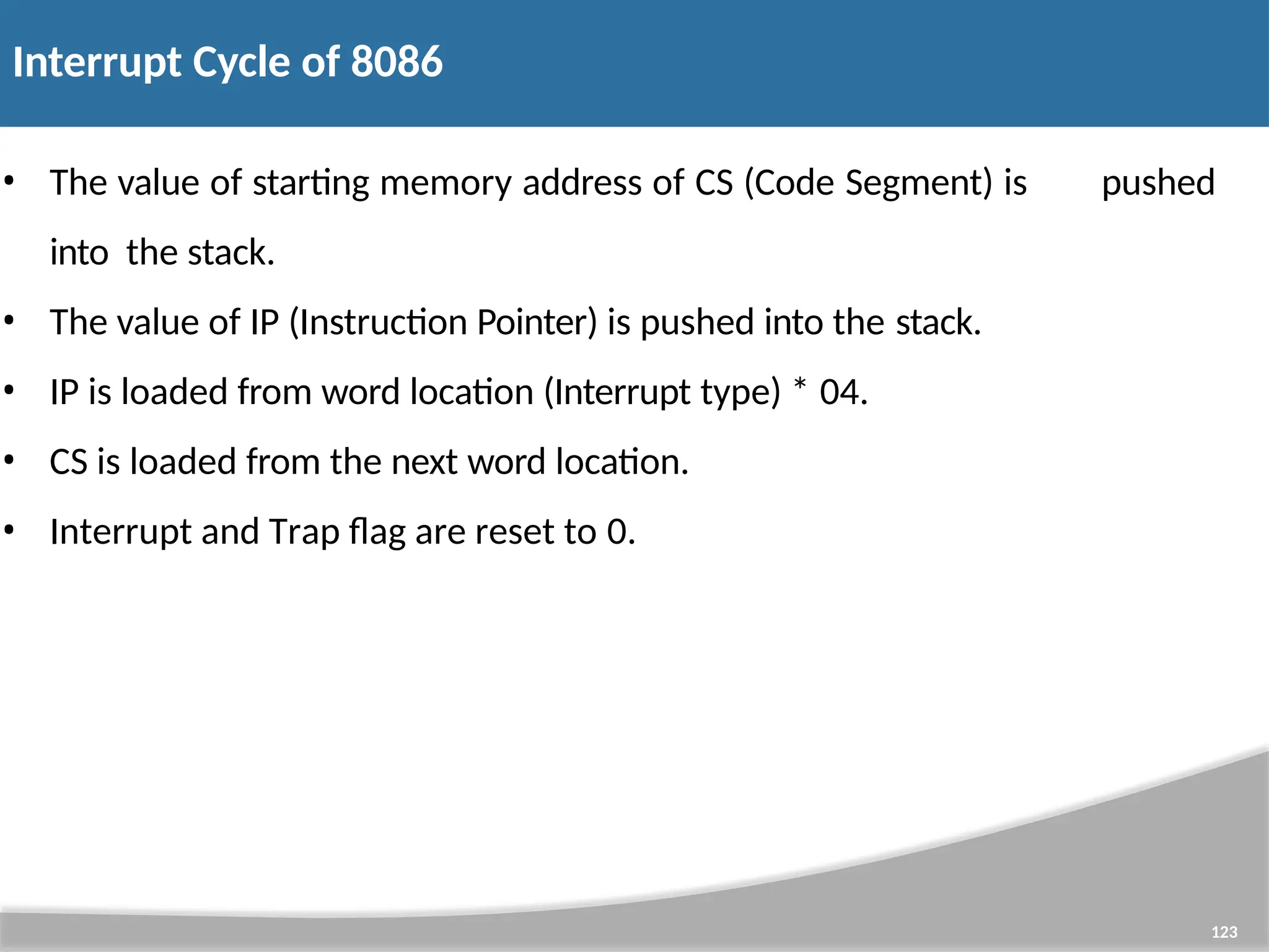
123.
Interrupt Cycle of8086 123 • The value of starting memory address of CS (Code Segment) is pushed into the stack. • The value of IP (Instruction Pointer) is pushed into the stack. • IP is loaded from word location (Interrupt type) * 04. • CS is loaded from the next word location. • Interrupt and Trap flag are reset to 0.
124.
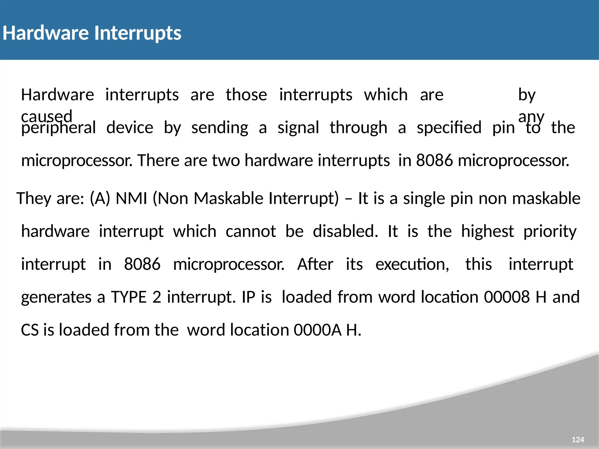
Hardware Interrupts 124 Hardware interruptsare those interrupts which are caused by any peripheral device by sending a signal through a specified pin to the microprocessor. There are two hardware interrupts in 8086 microprocessor. They are: (A) NMI (Non Maskable Interrupt) – It is a single pin non maskable hardware interrupt which cannot be disabled. It is the highest priority interrupt in 8086 microprocessor. After its execution, this interrupt generates a TYPE 2 interrupt. IP is loaded from word location 00008 H and CS is loaded from the word location 0000A H.
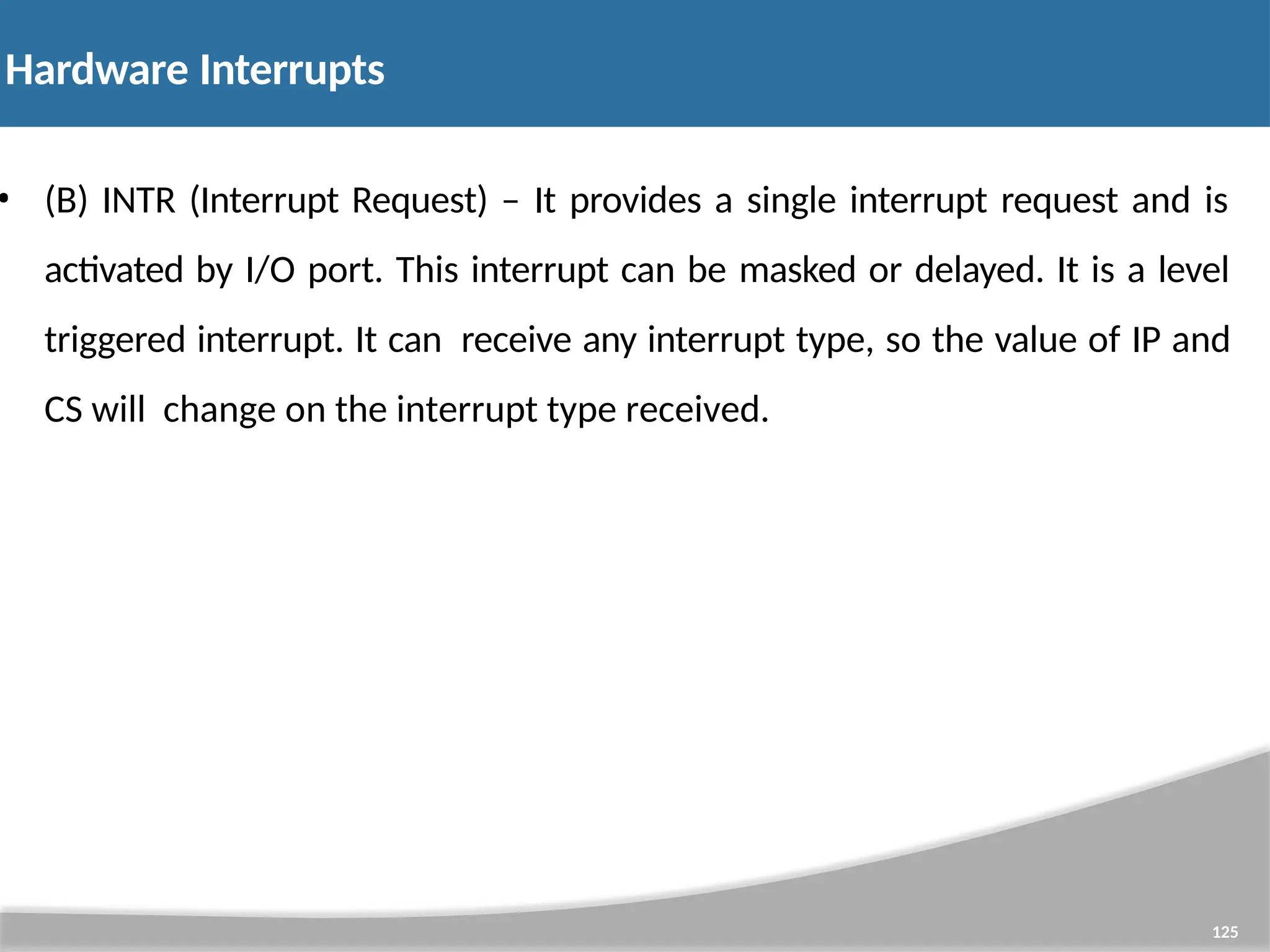
125.
Hardware Interrupts 125 • (B)INTR (Interrupt Request) – It provides a single interrupt request and is activated by I/O port. This interrupt can be masked or delayed. It is a level triggered interrupt. It can receive any interrupt type, so the value of IP and CS will change on the interrupt type received.
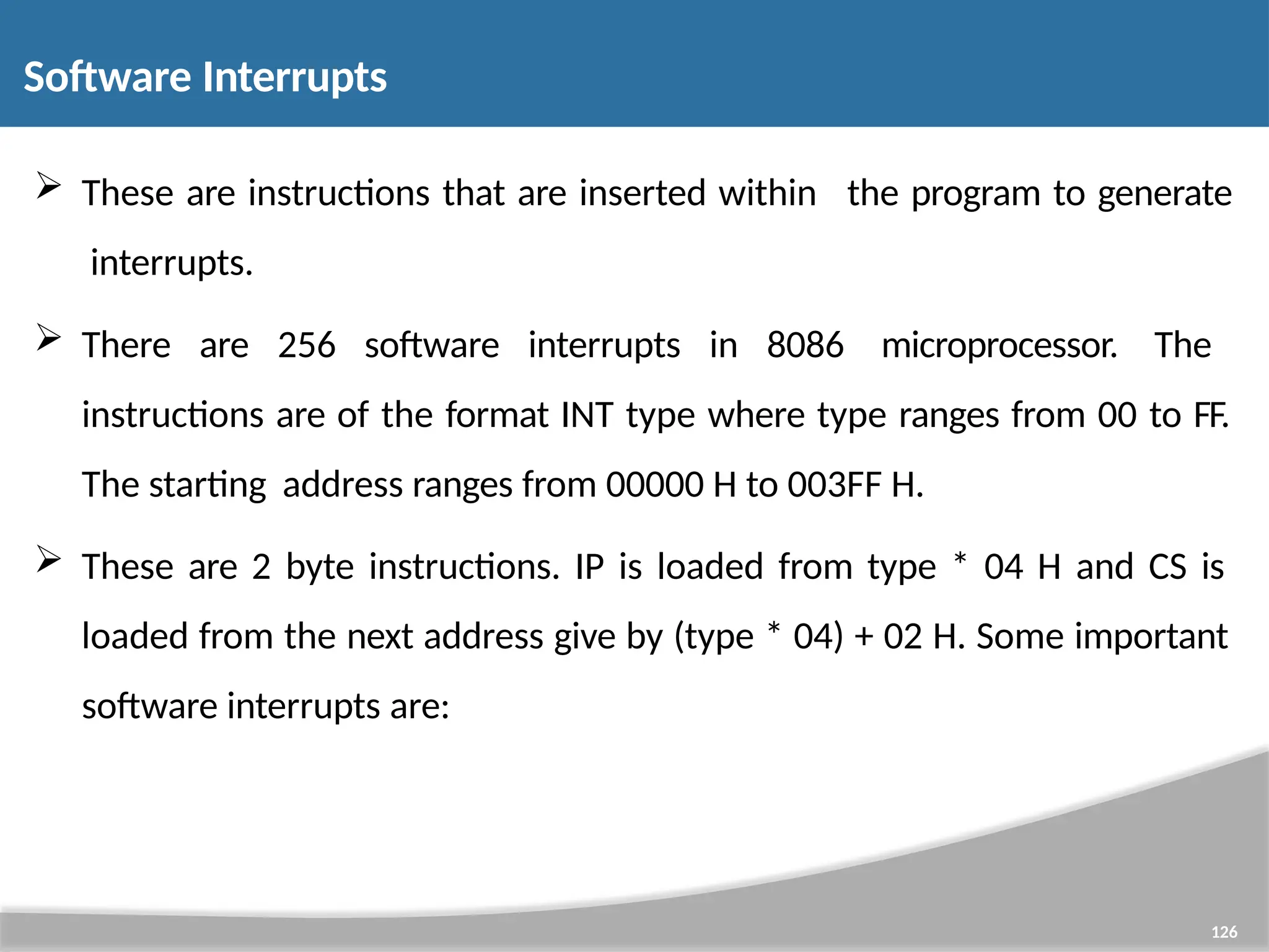
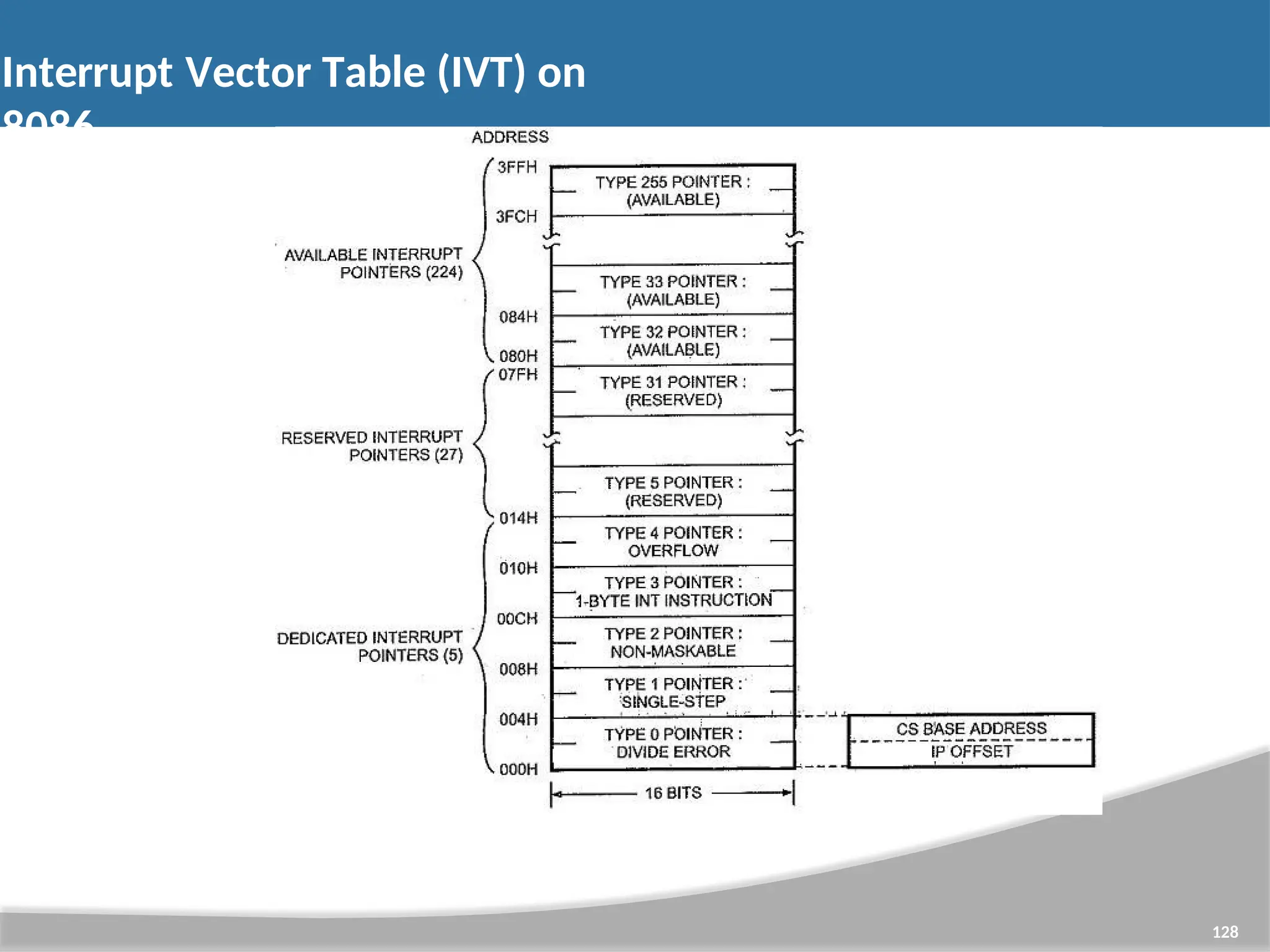
126.
These areinstructions that are inserted within interrupts. 126 the program to generate There are 256 software interrupts in 8086 microprocessor. The instructions are of the format INT type where type ranges from 00 to FF. The starting address ranges from 00000 H to 003FF H. These are 2 byte instructions. IP is loaded from type * 04 H and CS is loaded from the next address give by (type * 04) + 02 H. Some important software interrupts are: Software Interrupts
127.
TYPE 0 correspondsto division by zero(0). (A) TYPE 1 is used for single step execution for debugging of program. (B) TYPE 2 represents NMI and is used in power failure conditions. (C) TYPE 3 represents a break-point interrupt. (D) TYPE 4 is the overflow interrupt. 127 Software Interrupts
Non Maskable Interrupt 129 •Hardware interrupt is caused by any peripheral device by sending a signal through a specified pin to the microprocessor. The 8086 has two hardware interrupt pins, i.e. NMI and INTR. NMI is a non- maskable interrupt and INTR is a maskable interrupt having lower priority. • t is a single non-maskable interrupt pin (NMI) having higher priority than the maskable interrupt request pin (INTR)and it is of type 2 interrupt. • When this interrupt is activated, these actions take place − • Completes the current instruction that is in progress. • Pushes the Flag register values on to the stack.
130.
Non Maskable Interrupt 130 •Pushes the CS (code segment) value and IP (instruction pointer) of the return address on to the stack. • IP is loaded from the contents of the word location 00008H. • CS is loaded from the contents of the next word location 0000AH. • Interrupt flag and trap flag are reset to 0. value
131.
Maskable Interrupt 131 • The8086 has two hardware interrupt pins, i.e. ... NMI is a non-maskable interrupt and INTR is a maskable interrupt having lower priority. One moreinterrupt pin associated is INTA called interrupt acknowledge. • The INTR is a maskable interrupt because the microprocessor will be interrupted only if interrupts are enabled using set interrupt flag instruction. It should not be enabled using clear interrupt Flag instruction. • The INTR interrupt is activated by an I/O port. If the interrupt is enabled and NMI is disabled, then the microprocessor first completes the current execution and sends ‘0’ on INTA pin twice.
132.
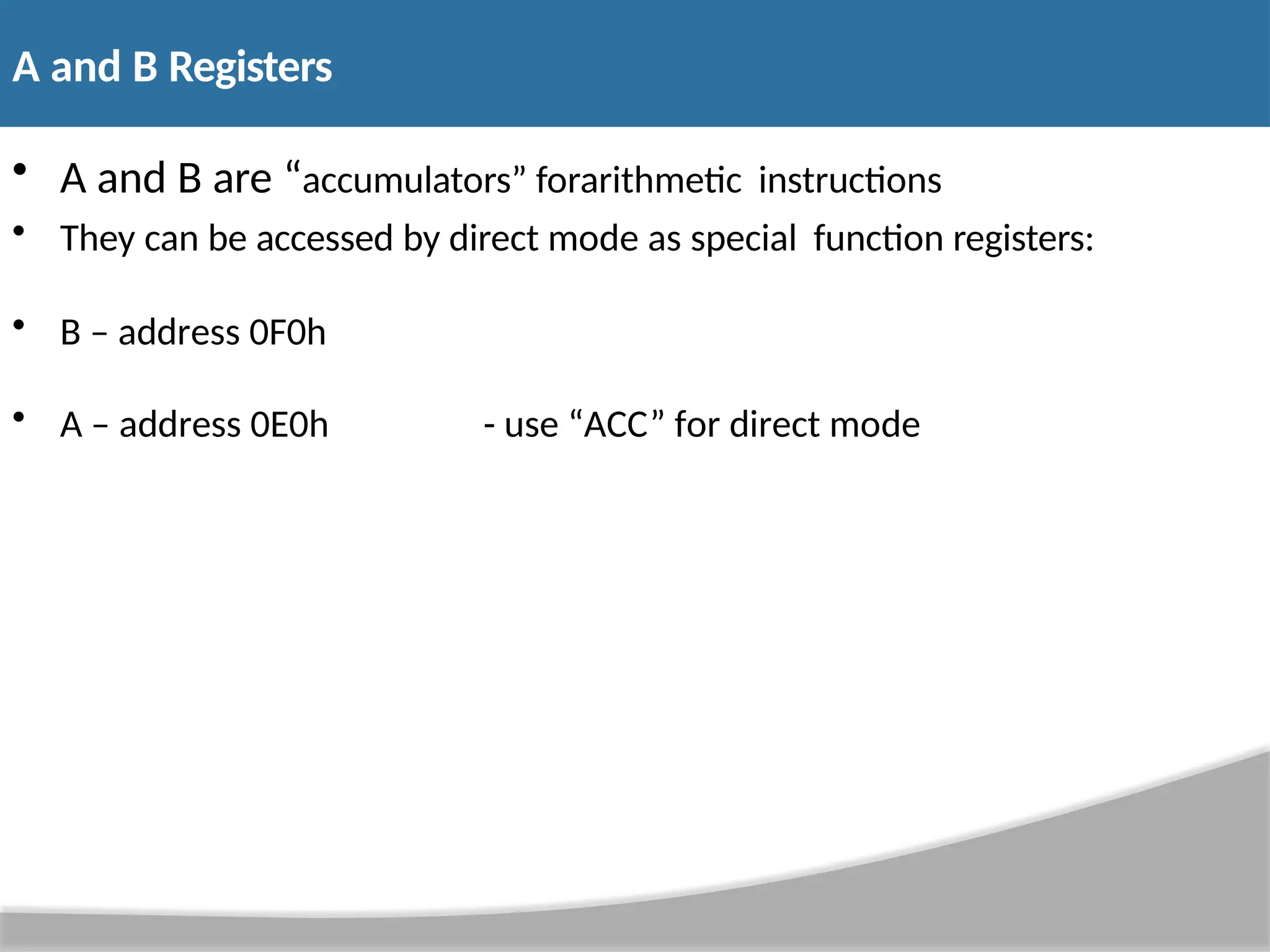
Maskable Interrupt 132 • Thefirst ‘0’ means INTA informs the external device to get ready and during the second ‘0’ the microprocessor receives the 8 bit, say X, from the programmable interrupt controller. • These actions are taken by the microprocessor − • First completes the current instruction. • Activates INTA output and receives the interrupt type, say X. • Flag register value, CS value of the return address and IP value of the return address are pushed on to the stack. • IP value is loaded from the contents of word location X × 4 • CS is loaded from the contents of the next word location. • Interrupt flag and trap flag is reset to 0
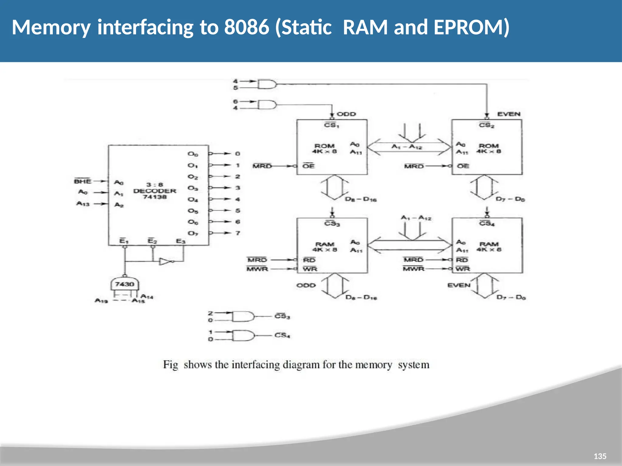
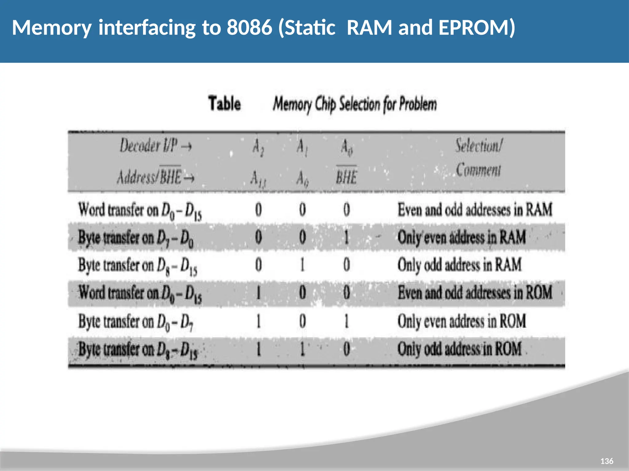
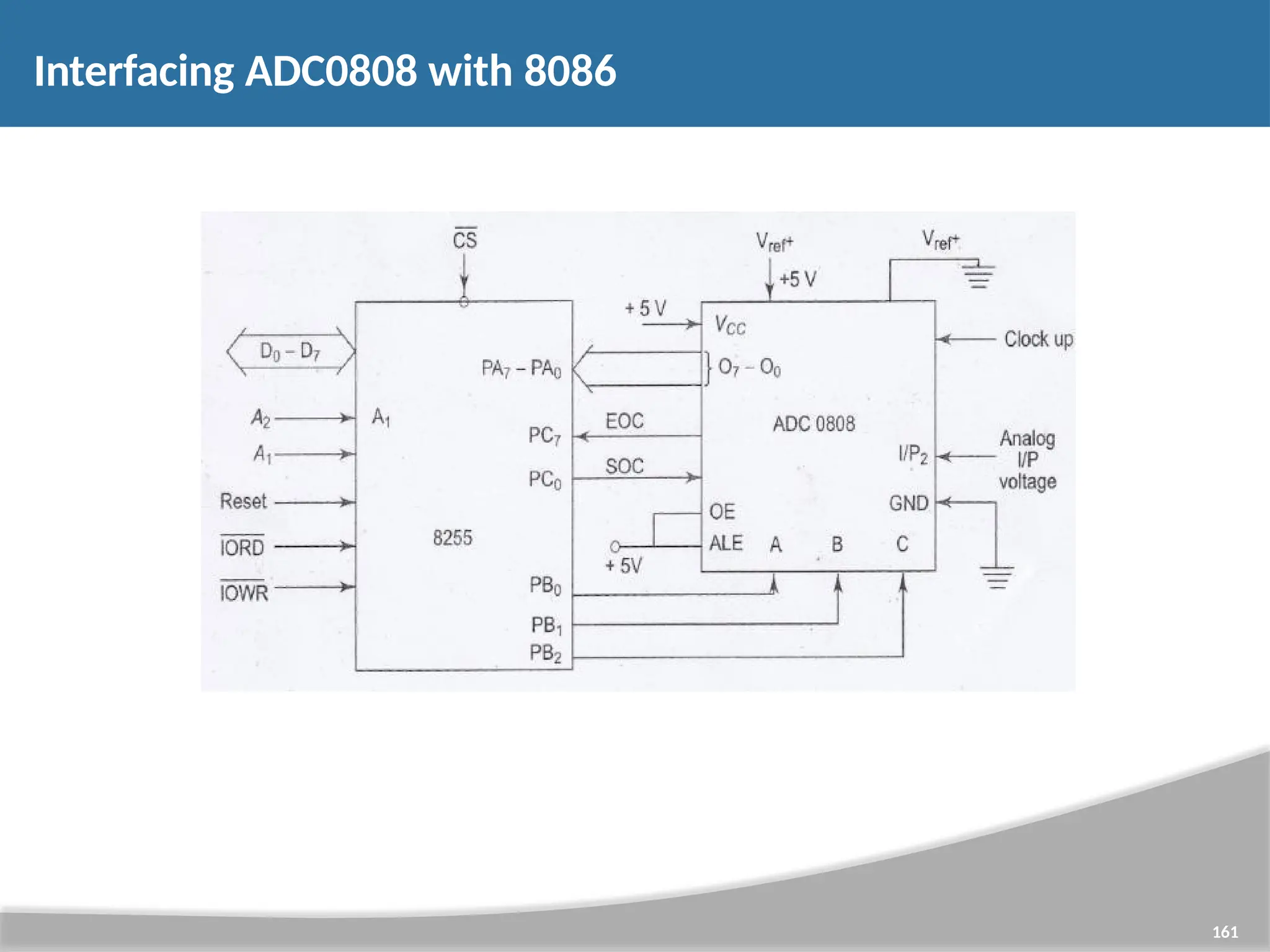
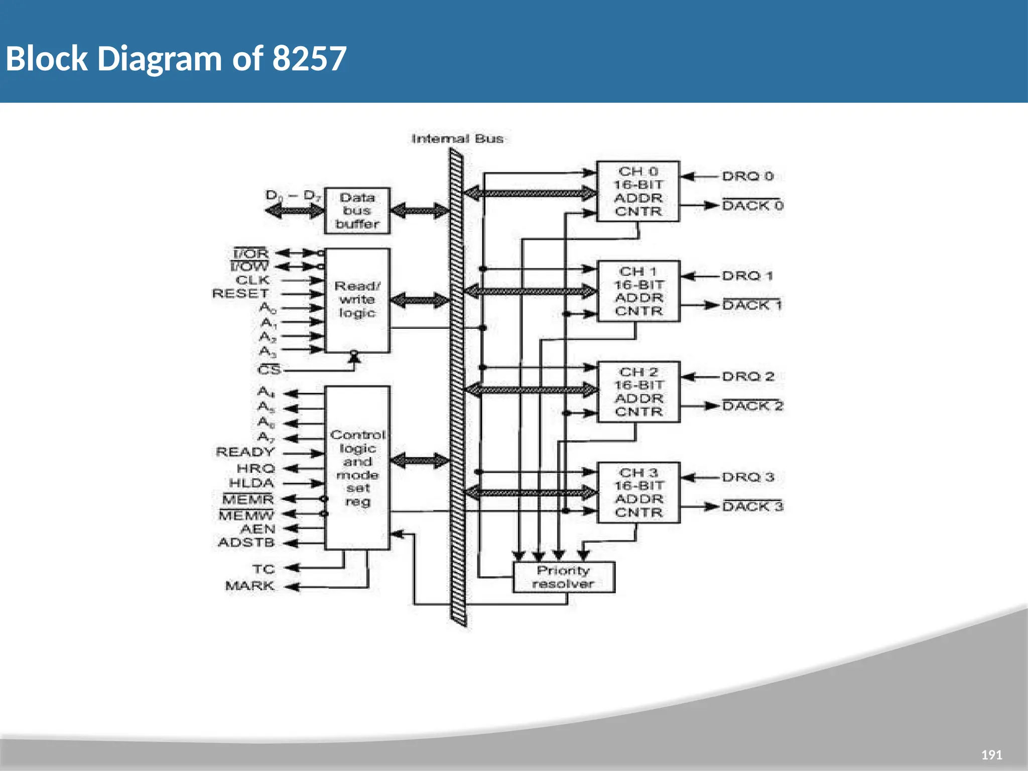
8255- PROGRAMMABLE PERIPHERALINTERFACE 84 191 It has 24 input/output lines 24 lines divided into 3 ports • Port A(8bit) • Port B(8 bit) • Port C upper(4 bit), Port C Lower (4 bit) All the above 3 ports can act as input or output ports
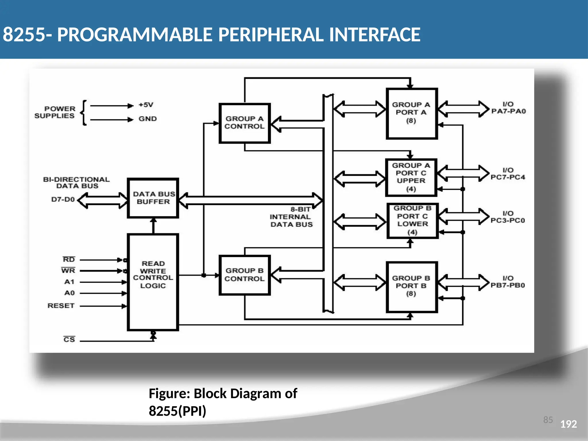
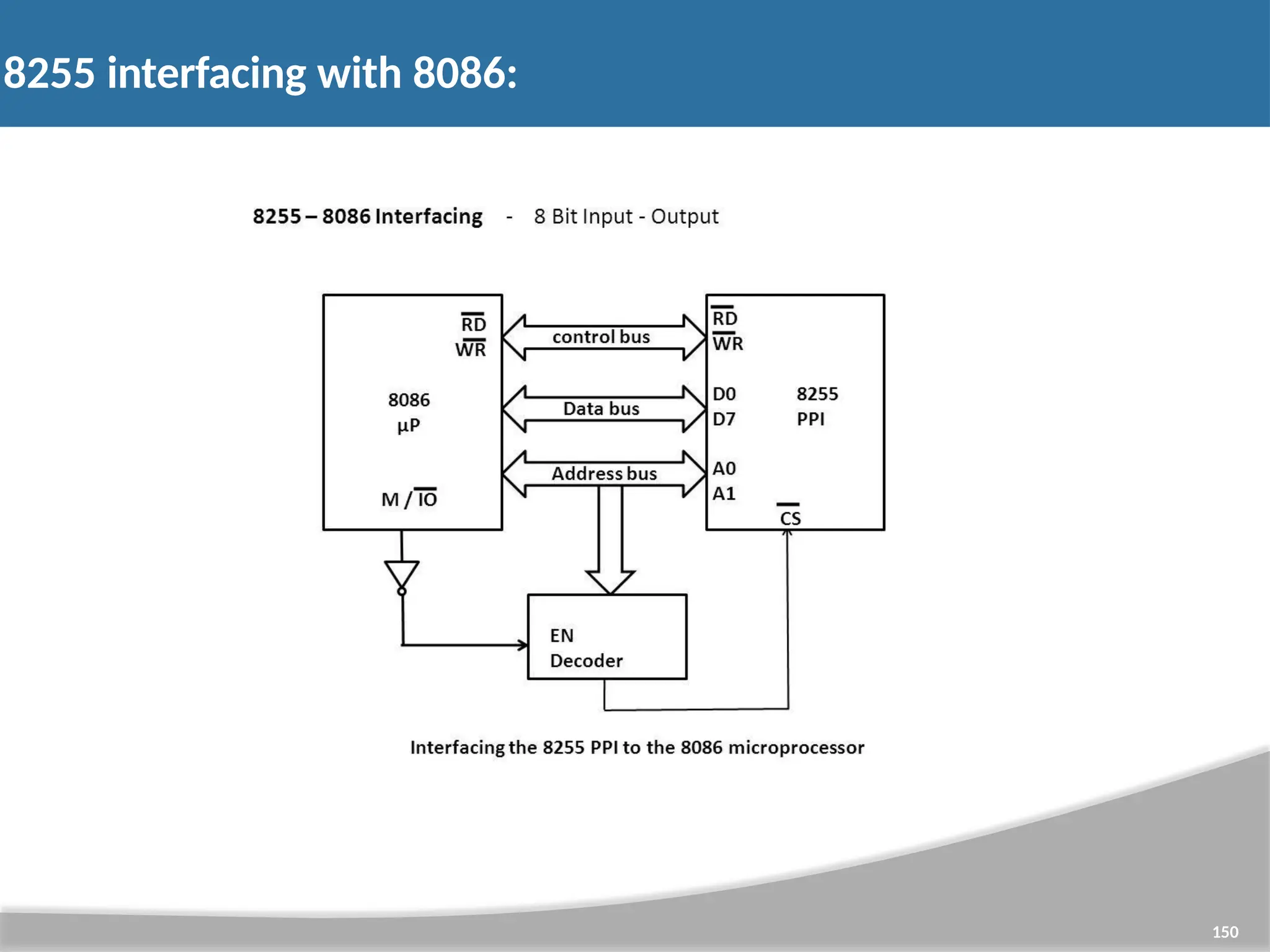
Data Bus buffer It is a 8-bit bidirectional Data bus. Used to interface between 8255 data bus with system bus. The internal data bus and Outer pins D0-D7 pins are connected in internally. The direction of data buffer is decided by Read/Control Logic. 86 193 8255- PROGRAMMABLE PERIPHERAL INTERFACE
140.
Read/Write Control Logic Thisis getting the input signals from control bus and Control signal are RD andWR. Address signals are A0, A1, and CS Address Bus. 8255 operation is enabledor disabled by CS. Group A and B get the Control Signal from CPU and send the command to the individual control blocks. Group A send the control signal to port A and Port C (Upper) PC7- PC4. Group B send the control signal to port B and Port C (Lower) PC3- PC0. 8255- PROGRAMMABLE PERIPHERAL INTERFACE 87 194
141.
PORT A: Thisis a 8-bit buffered I/O latch. It can be programmed by mode 0 , mode 1, mode 2 . PORT B: This is a 8-bit buffer I/O latch. It can be programmed by mode 0 and mode 1. PORTC: This is a 8-bit Unlatched buffer Input and an Output latch. It is spitted into two parts. It can be programmed by bit set/reset operation. 88 195 8255- PROGRAMMABLE PERIPHERAL INTERFACE
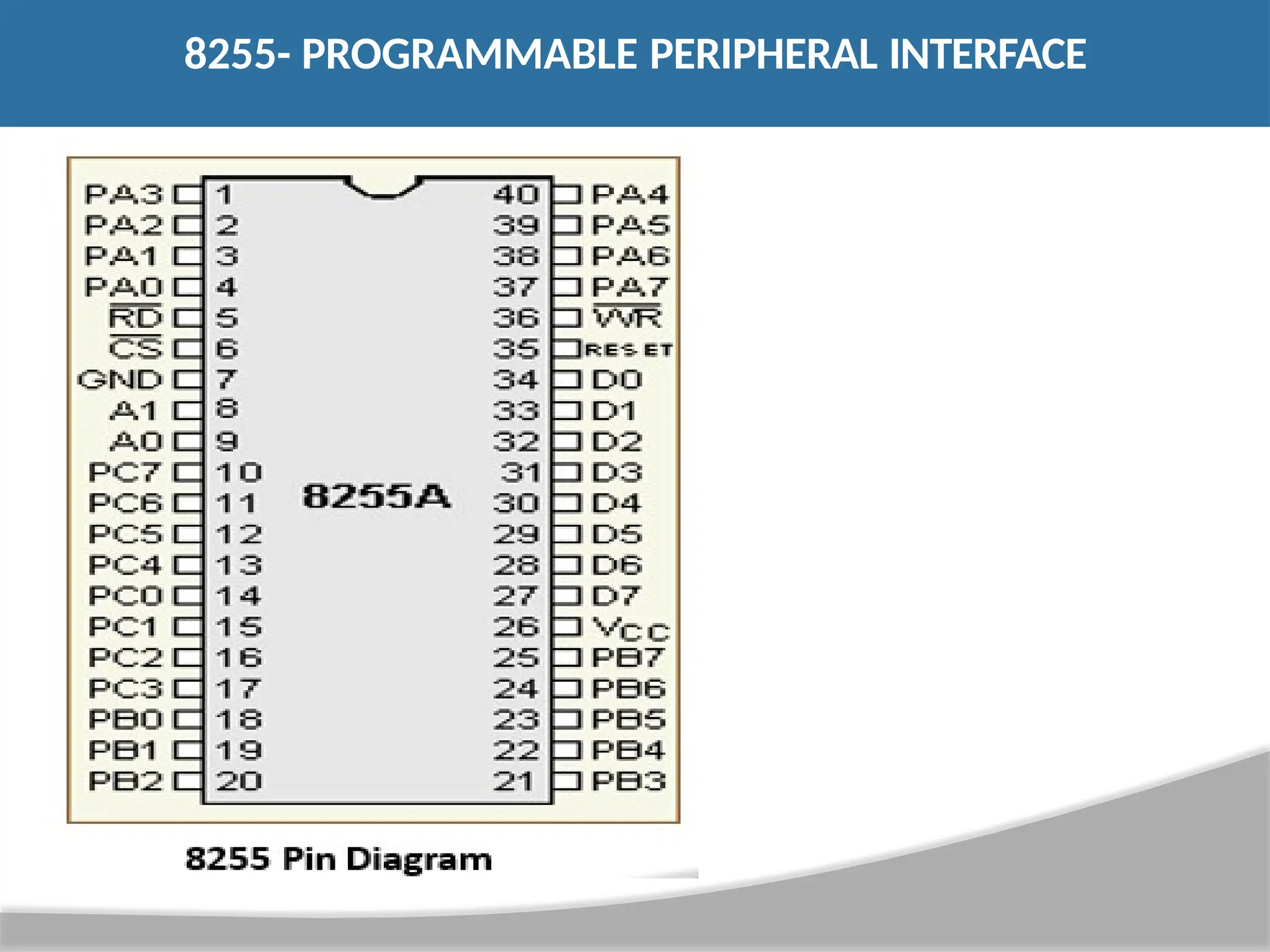
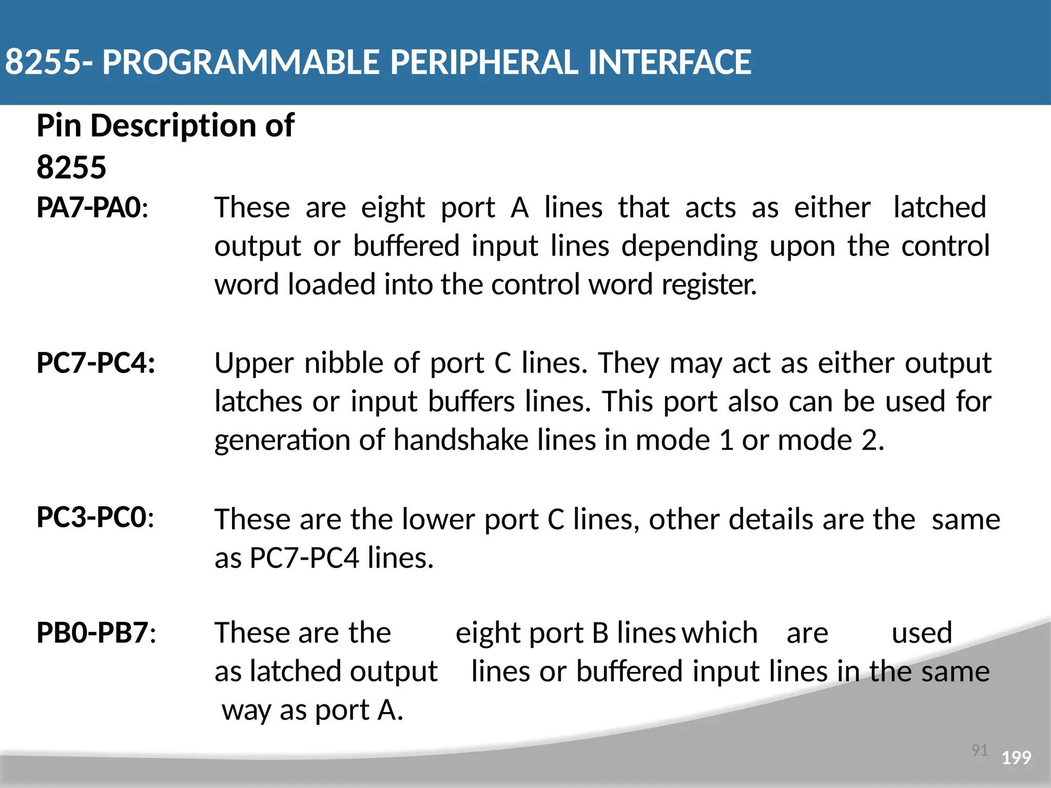
Pin Description of 8255 91199 PA7-PA0: These are eight port A lines that acts as either latched output or buffered input lines depending upon the control word loaded into the control word register. PC7-PC4: PC3-PC0: Upper nibble of port C lines. They may act as either output latches or input buffers lines. This port also can be used for generation of handshake lines in mode 1 or mode 2. These are the lower port C lines, other details are the same as PC7-PC4 lines. PB0-PB7: eight port B lineswhich are used lines or buffered input lines in the same These are the as latched output way as port A. 8255- PROGRAMMABLE PERIPHERAL INTERFACE
144.
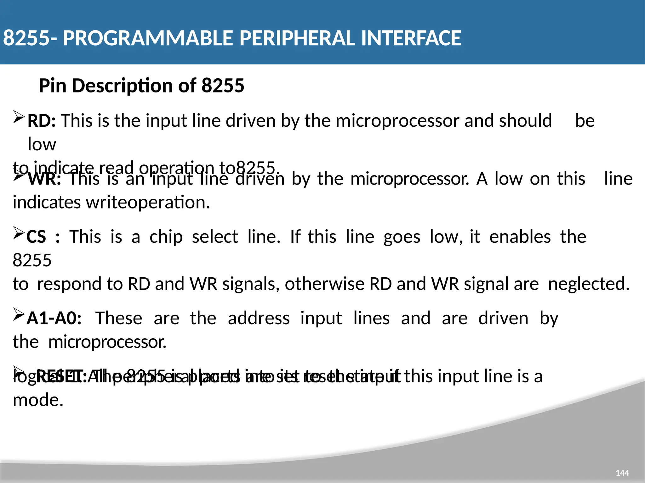
Pin Description of8255 RD: This is the input line driven by the microprocessor and should be low to indicate read operation to8255. 144 line WR: This is an input line driven by the microprocessor. A low on this indicates writeoperation. CS : This is a chip select line. If this line goes low, it enables the 8255 to respond to RD and WR signals, otherwise RD and WR signal are neglected. A1-A0: These are the address input lines and are driven by the microprocessor. RESET: The 8255 is placed into its reset state if this input line is a logical 1. All peripheral ports are set to the input mode. 8255- PROGRAMMABLE PERIPHERAL INTERFACE
145.
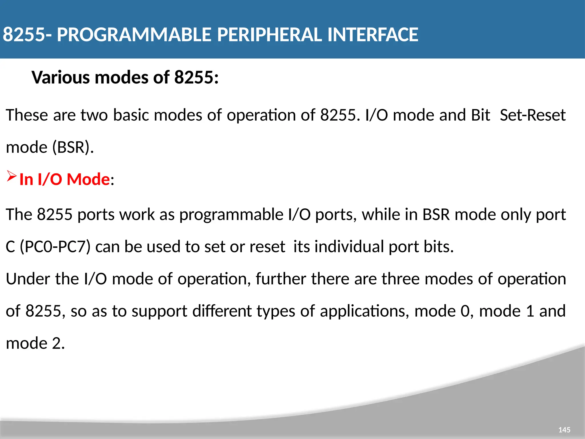
Various modes of8255: These are two basic modes of operation of 8255. I/O mode and Bit Set-Reset mode (BSR). In I/O Mode: The 8255 ports work as programmable I/O ports, while in BSR mode only port C (PC0-PC7) can be used to set or reset its individual port bits. Under the I/O mode of operation, further there are three modes of operation of 8255, so as to support different types of applications, mode 0, mode 1 and mode 2. 145 8255- PROGRAMMABLE PERIPHERAL INTERFACE
146.
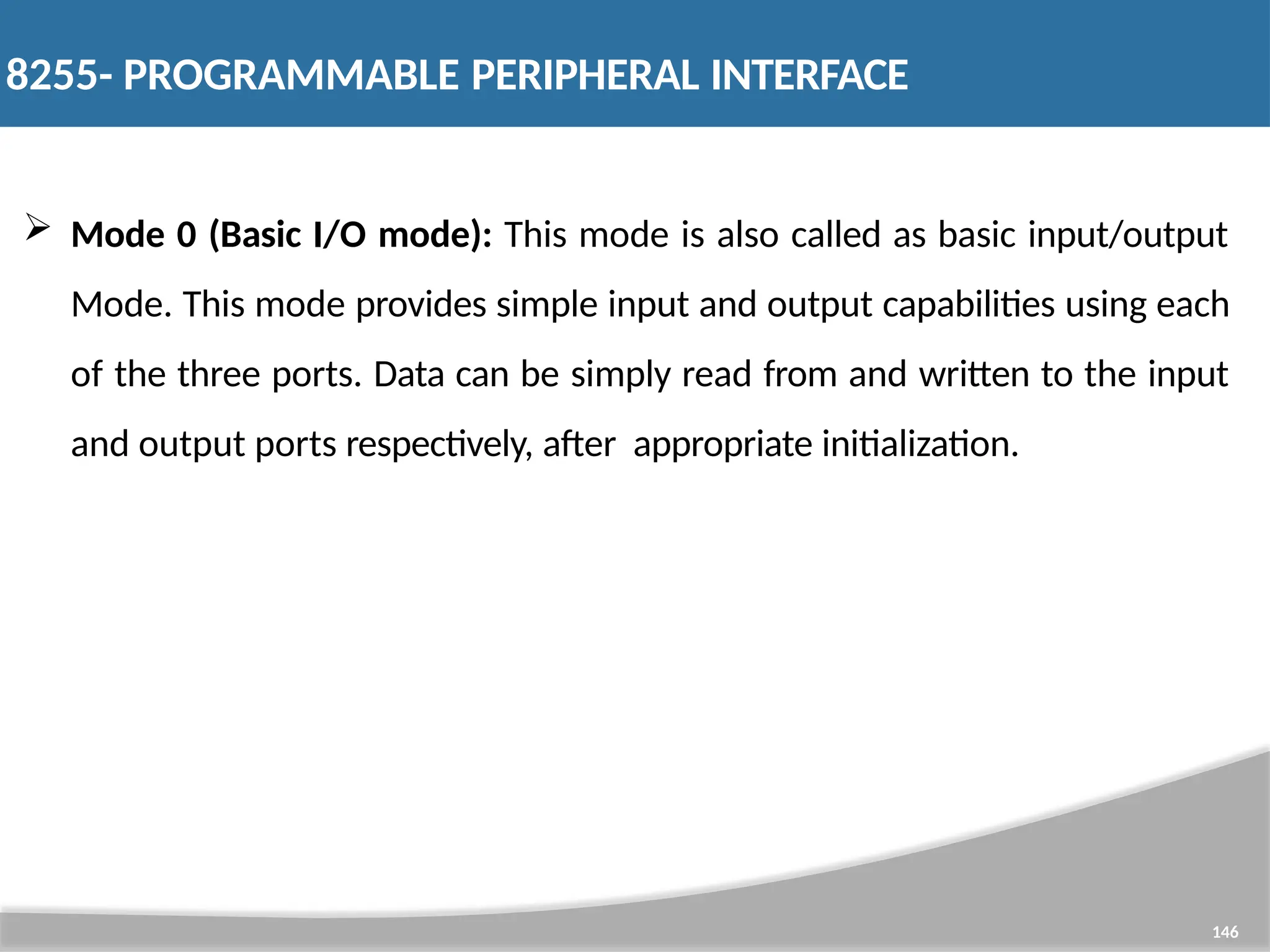
Mode 0(Basic I/O mode): This mode is also called as basic input/output Mode. This mode provides simple input and output capabilities using each of the three ports. Data can be simply read from and written to the input and output ports respectively, after appropriate initialization. 146 8255- PROGRAMMABLE PERIPHERAL INTERFACE
147.
Mode 1: (Strobedinput/output mode) in this mode the handshaking control the input and output action of the specified port. Port C lines PC0- PC2, provide strobe or handshake lines for port B. This group which includes port B and PC0-PC2 is called as group B for Strobed data input/output. Port C lines PC3-PC5 provides strobe lines for port A. This group including port A and PC3-PC5 from group A. Thus port C is utilized for generating handshake signals. 147 8255- PROGRAMMABLE PERIPHERAL INTERFACE
148.
Mode 2(Strobed bidirectional I/O): This mode of operation of 8255 is also called as strobed bidirectional I/O. This mode of operation provides 8255 with additional features for communicating with a peripheral device on an 8-bit data bus. 148 Handshaking signals are provided to maintain proper synchronization between the data transmitter and receiver. data flow and The interrupt generation and other functions are similar to mode 1. 8255- PROGRAMMABLE PERIPHERAL INTERFACE
149.
BSR Mode: Inthis mode any of the 8-bits of port C can be set or reset depending on D0 of the control word. The bit to be set or reset is selected by bit select flags D3, D2 and D1 of the CWR as given in table. 149 8255- PROGRAMMABLE PERIPHERAL INTERFACE
Stepper motoris often used in computer systems. Normally DC and AC motors move smoothly in a circular fashion. Stepper motor is a DC motor, specially designed, which moves in discrete or fixed step and thus complete one rotation of 360 degrees. To rotate the shaft of the motor a sequence of pulses are applied to the windings in a predefined sequence. The number of pulses required to complete one rotation depends on the number of teeth on the rotor. Hence rotation Per pulse sequence is 3600/NT where NT is the number of teeth on rotor. 151 Stepper motor
152.
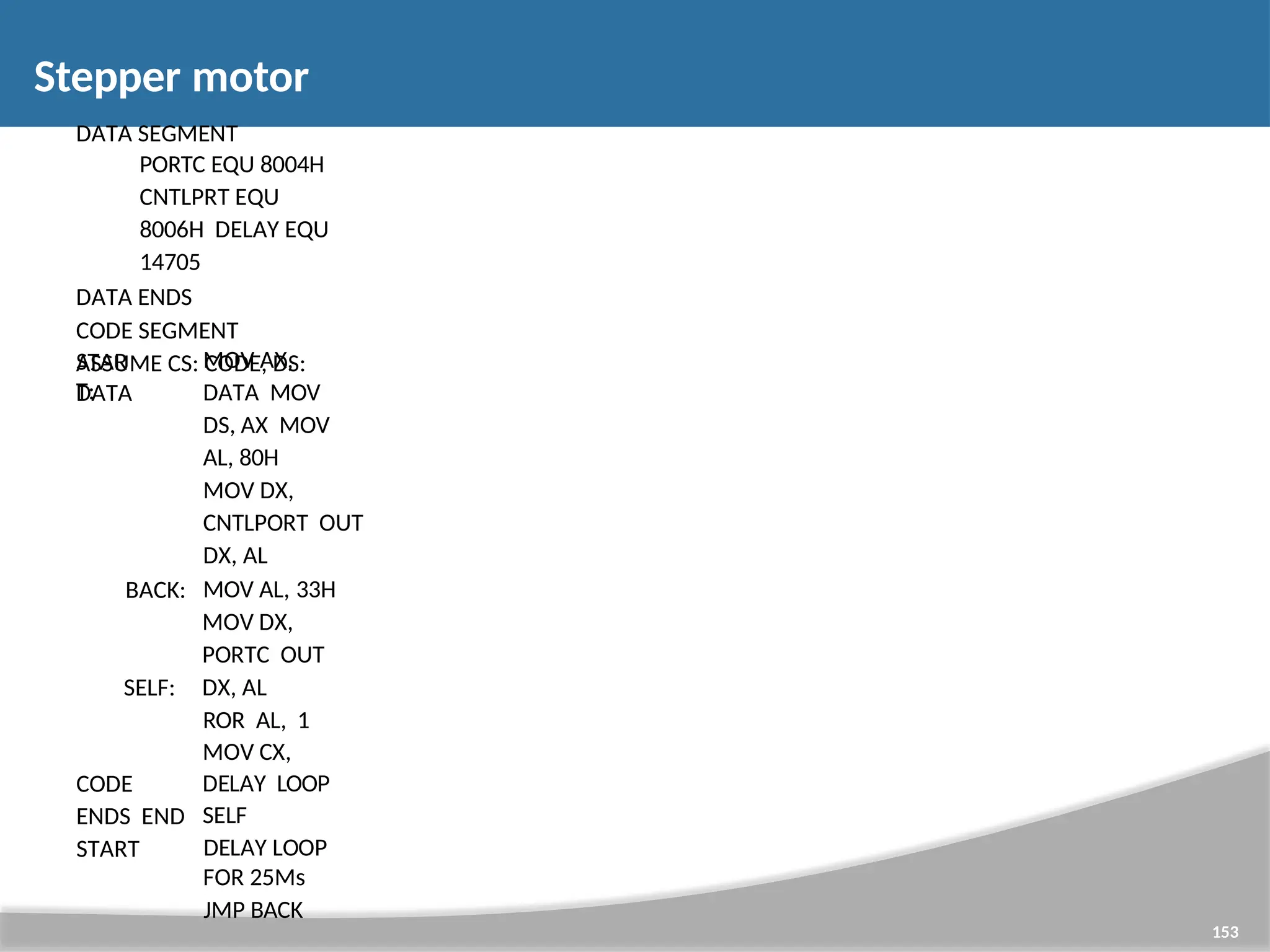
Programs for StepperMotor Rotation: 1. Program to rotate the stepper motor continuously in clockwise direction for following specification NT = Number of teeth on rotor = 200 Speed of motor = 12 rotations/minute. CPU frequency = 10MHz 152 Stepper motor
153.
DATA SEGMENT PORTC EQU8004H CNTLPRT EQU 8006H DELAY EQU 14705 DATA ENDS CODE SEGMENT ASSUME CS: CODE, DS: DATA 153 STAR T: BACK: SELF: MOV AX, DATA MOV DS, AX MOV AL, 80H MOV DX, CNTLPORT OUT DX, AL MOV AL, 33H MOV DX, PORTC OUT DX, AL ROR AL, 1 MOV CX, DELAY LOOP SELF DELAY LOOP FOR 25Ms JMP BACK CODE ENDS END START Stepper motor
154.
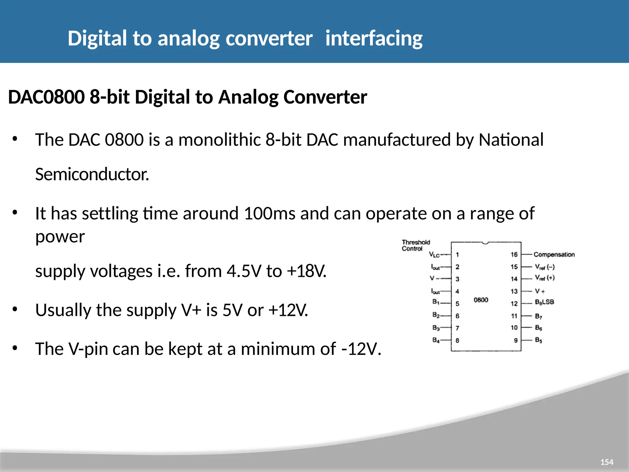
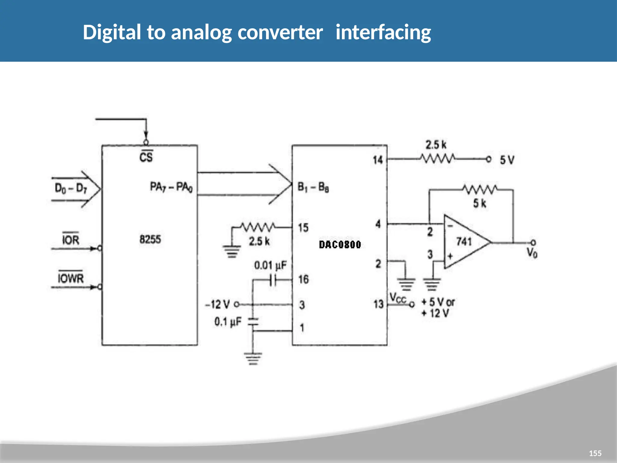
DAC0800 8-bit Digitalto Analog Converter • The DAC 0800 is a monolithic 8-bit DAC manufactured by National Semiconductor. • It has settling time around 100ms and can operate on a range of power supply voltages i.e. from 4.5V to +18V. • Usually the supply V+ is 5V or +12V. • The V-pin can be kept at a minimum of -12V. Digital to analog converter interfacing 154
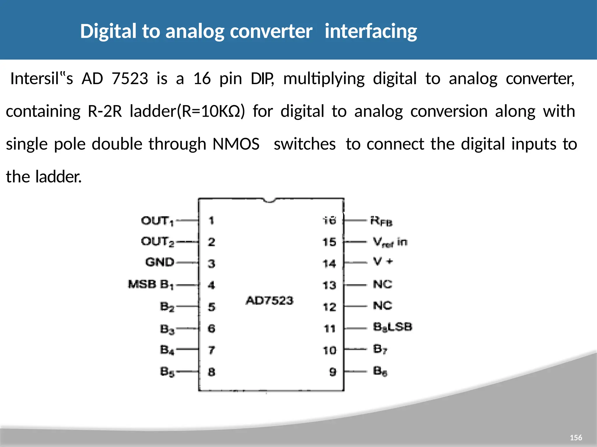
Intersil‟s AD 7523is a 16 pin DIP, multiplying digital to analog converter, containing R-2R ladder(R=10KΩ) for digital to analog conversion along with single pole double through NMOS switches to connect the digital inputs to the ladder. converter n ci 156 Digital to analog converter interfacing
157.
Pin Diagram ofAD7523 157 • The supply range extends from +5V to +15V , while Vref may be anywhere between -10V to +10V. The maximum analog output voltage will be +10V, when all the digital inputs are at logic high state. Usually a Zener is connected between OUT1 and OUT2 to save the DAC from negative transients. • An operational amplifier is used as a current to voltage converter at the output of AD 7523 to convert the current output of AD7523 to a proportional output voltage. • It also offers additional drive capability to the DAC output. An external feedback resistor acts to control the gain. One may not connect any external feedback resistor, if no gain control is required.
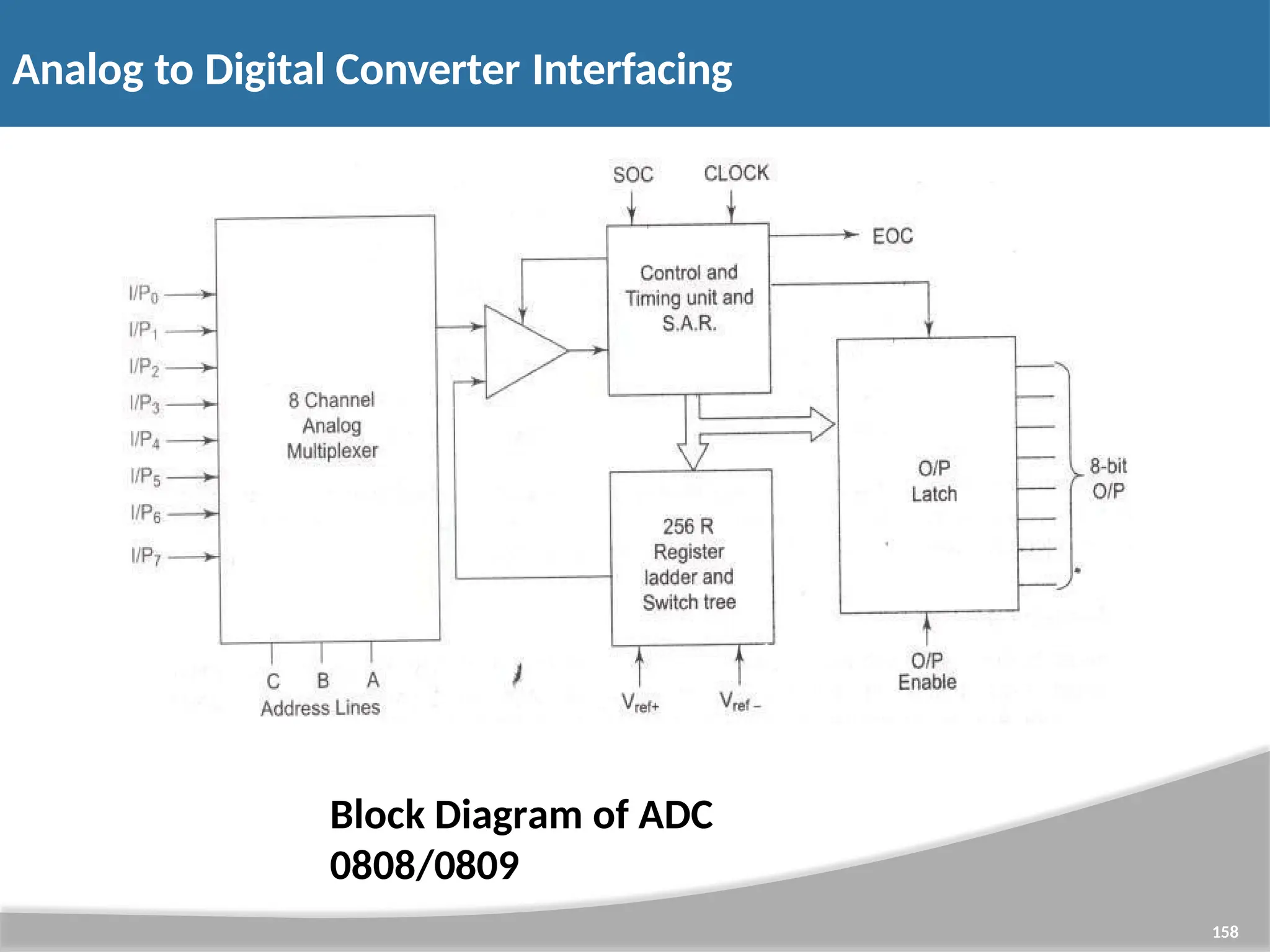
158.
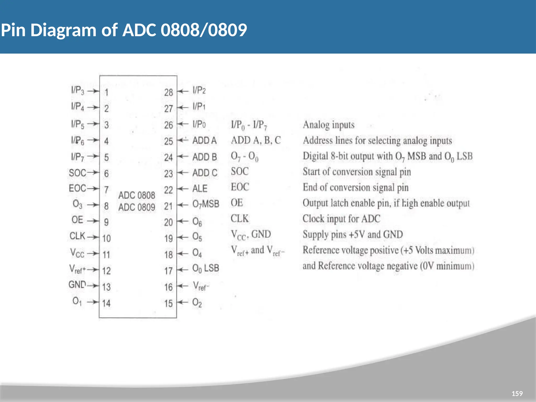
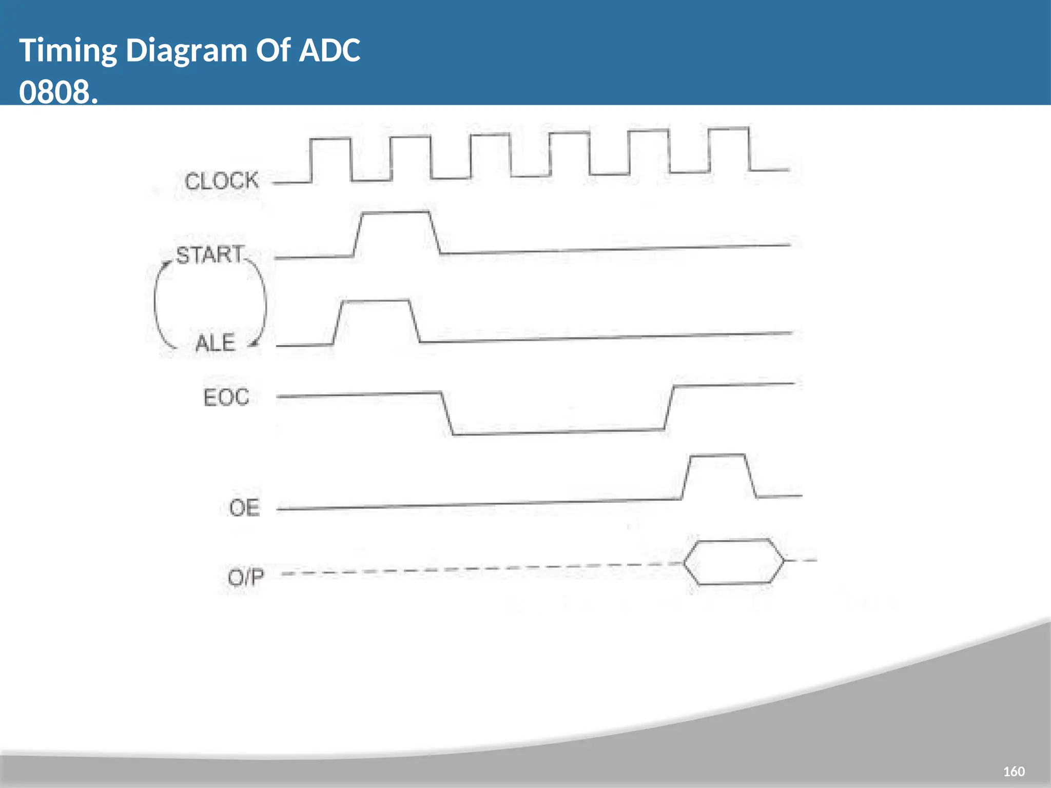
Block Diagram ofADC 0808/0809 Analog to Digital Converter Interfacing 158
Programmable interrupt controller8259A 162 • 8259 microprocessor is defined as Programmable Interrupt Controller (PIC) microprocessor. There are 5 hardware interrupts and 2 hardware interrupts in 8085 and 8086 respectively. • But by connecting 8259 with CPU, we can increase the interrupt handling capability. 8259 combines the multi interrupt input sources into a single interrupt output. Interfacing of single PIC provides 8 interrupts inputs from IR0-IR7. • For example, interfacing of 8085 and 8259 increases the interrupt handling capability of 8085 microprocessor from 5 to 8 interrupt levels.
163.
Features of 8259PIC microprocessor 163 • It is a LSI chip which manages 8 levels of interrupts i.e. it is used to implement 8 level interrupt systems. • It can be cascaded in a master slave configuration to handle up to 64 levels of interrupts. • It can identify the interrupting device. • It can resolve the priority of interrupt requests i.e. it does not require any external priority resolver. • It can be operated in various priority modes such as fixed priority and rotating priority. • The interrupt requests are individually mask-able.
164.
Features of 8259PIC microprocessor 164 • The operating modes and masks may be dynamically changed by the software at any time during execution of programs. • It accepts requests from the peripherals, determines priority of incoming request, checks whether the incoming request has a higher priority value than the level currently being serviced and issues an interrupt signal to the microprocessor. • It provides 8 bit vector number as an interrupt information. • It does not require clock signal. • It can be used in polled as well as interrupt modes. • The starting address of vector number is programmable. • It can be used in buffered mode
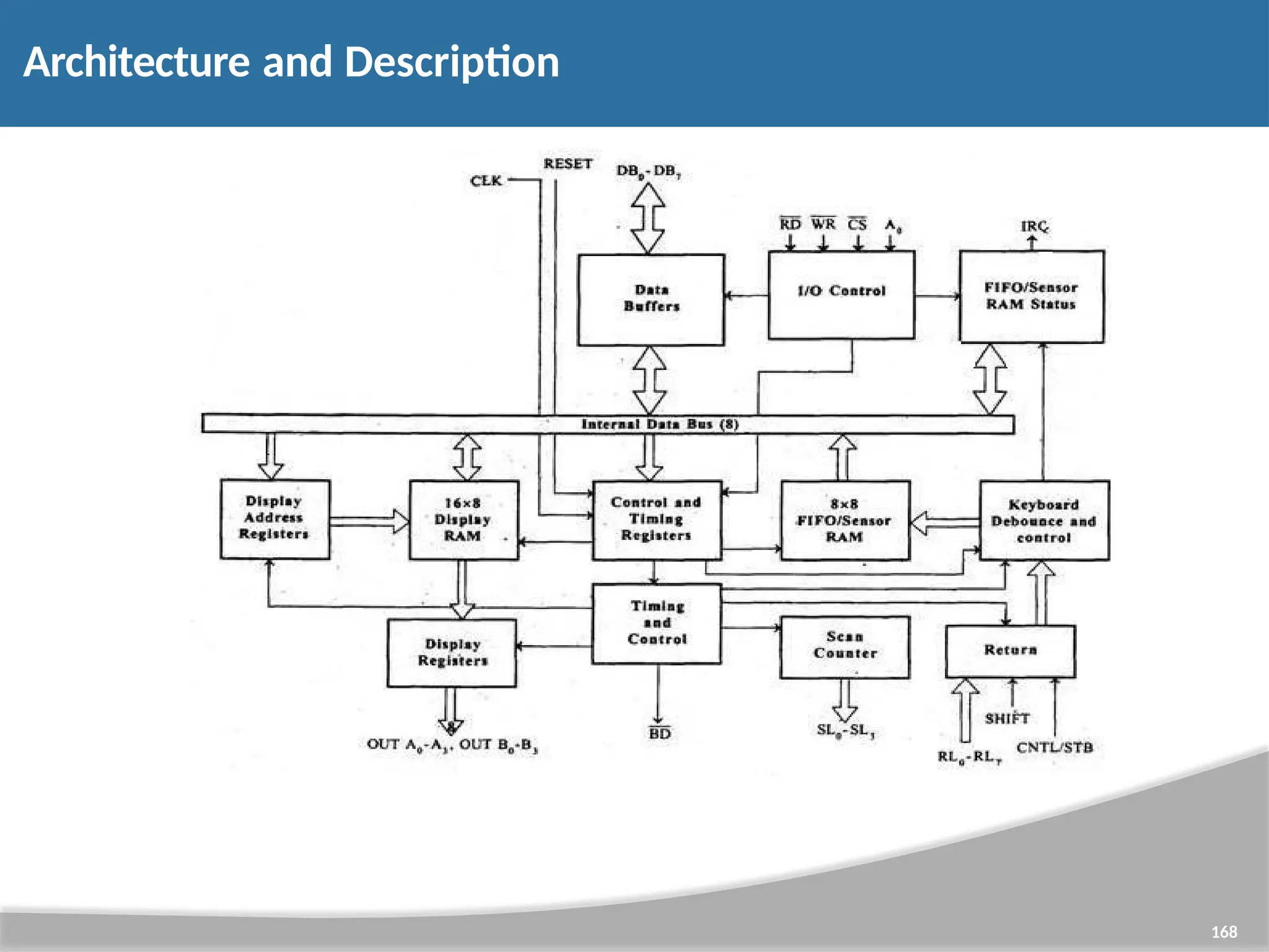
keyboard /display controller8279 167 8279programmable keyboard/display controller is designed by Intel that interfaces a keyboard with the CPU. The keyboard first scans the keyboard and identifies if any key has been pressed. It then sends their relative response of the pressed key to the CPU and vice-a-versa. How Many Ways the Keyboard is Interfaced with the CPU? The Keyboard can be interfaced either in the interrupt or the polled mode. In the Interrupt mode, the processor is requested service only if any key is pressed, otherwise the CPU will continue with its main task. In the Polled mode, the CPU periodically reads an internal flag of 8279 to check whether any key is pressed or not with key pressure.
• I/O Controland Data Buffer • This unit controls the flow of data through the microprocessor. It is enabled only when D is low. Its data buffer interfaces the external bus of the system with the internal bus of the microprocessor. The pins A0, RD, and WR are used for command, status or data read/write operations. • Control and Timing Register and Timing Control • This unit contains registers to store the keyboard, display modes, and other operations as programmed by the CPU. The timing and control unit handles the timings for the operation of the circuit. 169 Architecture and Description….
Programmable communication interface8251 USART 171 • Most of devices are parallel in nature. These devices transfer data simultaneously on data lines. But parallel data transfer process is very complicated and expensive. Hence in some situations the serial I/O mode is used where one bit is transferred over a single line at a time. In this type of transmission parallel word is converted into a stream of serial bits which is known as parallel to serial conversion. The rate of transmission in serial mode is BAUD, i.e., bits per second. The serial data transmission involves starting, end of transmission, error verification bits along with the data.
172.
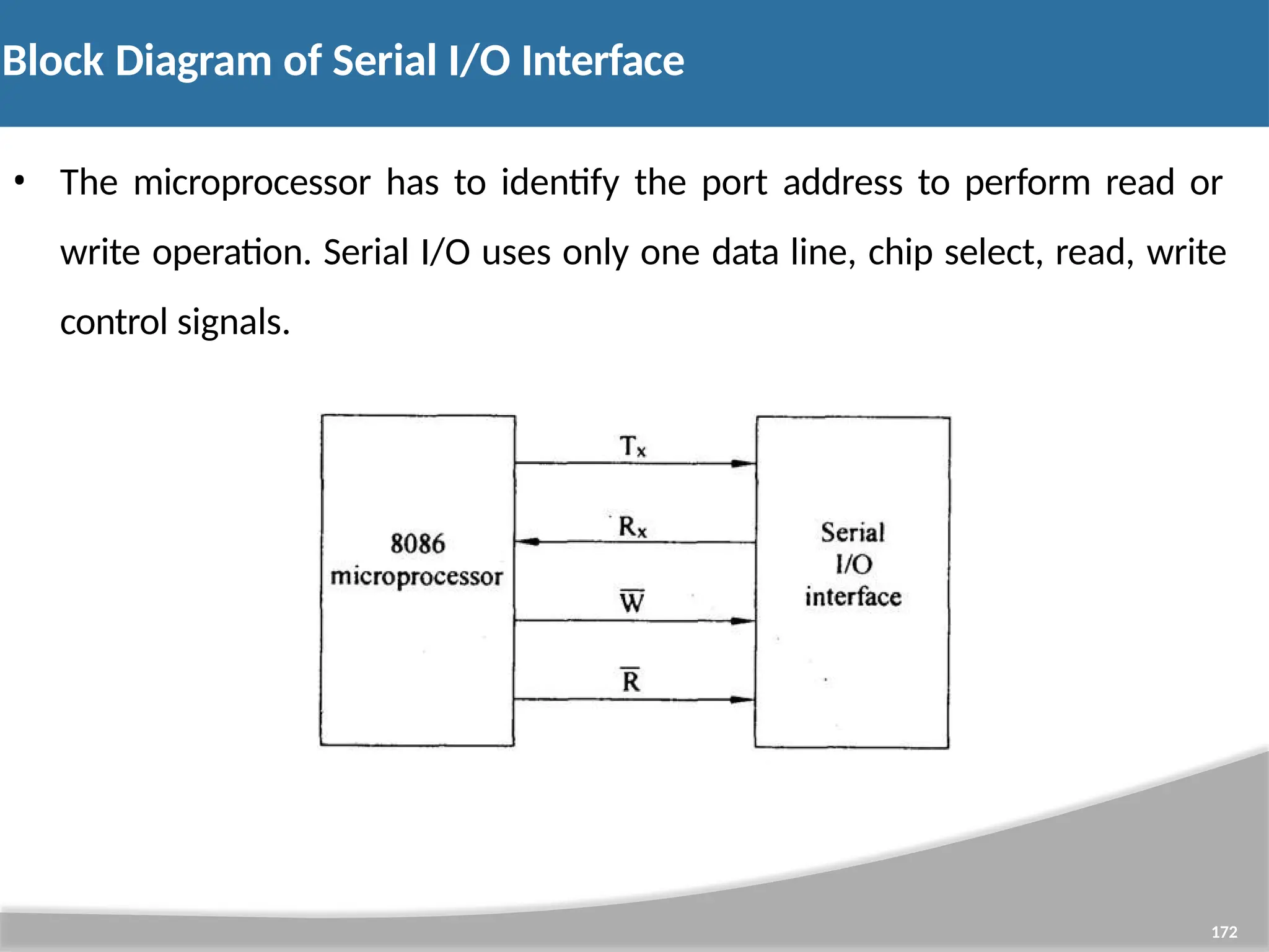
Block Diagram ofSerial I/O Interface • The microprocessor has to identify the port address to perform read or write operation. Serial I/O uses only one data line, chip select, read, write control signals. 172
173.
INTRODUCTION SERIAL COMMUNICATION 173 Serialcommunication is common method of transmitting data between a computer and a peripheral device such as a programmable instrument or even another computer. Serial communication transmits data one bit at a time, sequentially, over a single communication line to a receiver. Serial is also a most popular communication protocol that is used by many devices for instrumentation.
174.
Introduction Serial Communication 174 Thismethod is used when data transfer rates are very low or the data must be transferred over long distances and also where the cost of cable and synchronization difficulties makes parallel communication impractical. Serial communication is popular because most computers have one or more serial ports, so no extra hardware is needed other than a cable to connect the instrument to the computer or two computers together.
175.
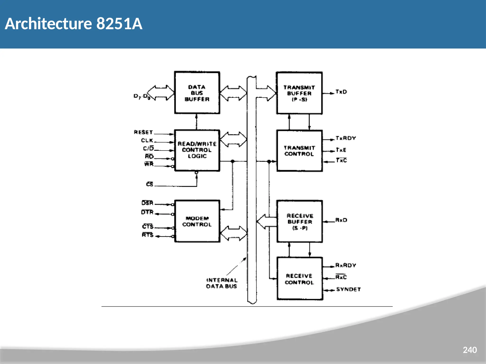
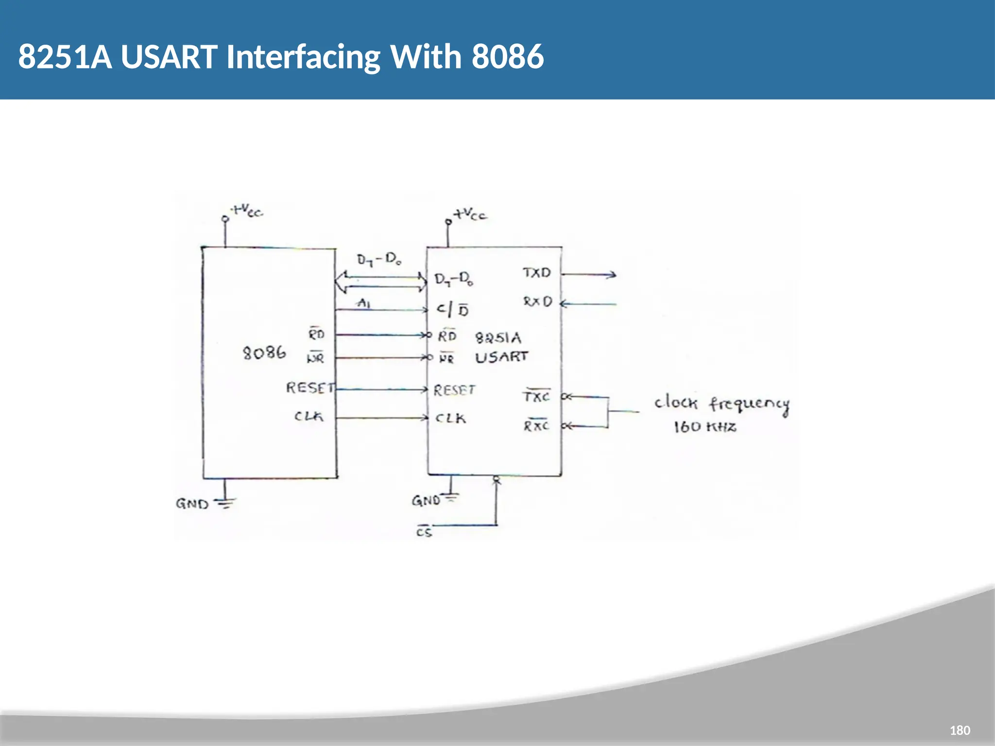
8251a-usart-universal Synchronous/Asynchronous Receiver/Transmitter 175 • AUSART is also called a programmable communications interface (PCI). When information is to be sent by 8086 over long distances, it is • economical to send it on a single line. The 8086 has to convert parallel data to serial data and then output it. Thus lot of microprocessor time is required for such a conversion. • Similarly, if 8086 receives serial data over long distances, the 8086 has to internally convert this into parallel data before processing it. Again, lot of time is required for such a conversion. The 8086 can delegate the job of conversion from serial to parallel and vice versa to the 8251A USART used in thesystem.
176.
8251A-USART-Universal Synchronous/Asynchronous Receiver/Transmitter 176 • TheIntel 8251A is the industry standard Universa l Synchronous/Asynchronous Receiver/Transmitter (USART), designed for data communications with Intel microprocessor families such as 8080, 85, 86 and • The 8251A converts the parallel data received from the processor on the D7-0 data pins into serial data, and transmits it on TxD (transmit data) output pin of 8251A. Similarly, it converts the serial data received on RxD (receive data) input into parallel data, and the processor reads it using the data pins D7-0.
177.
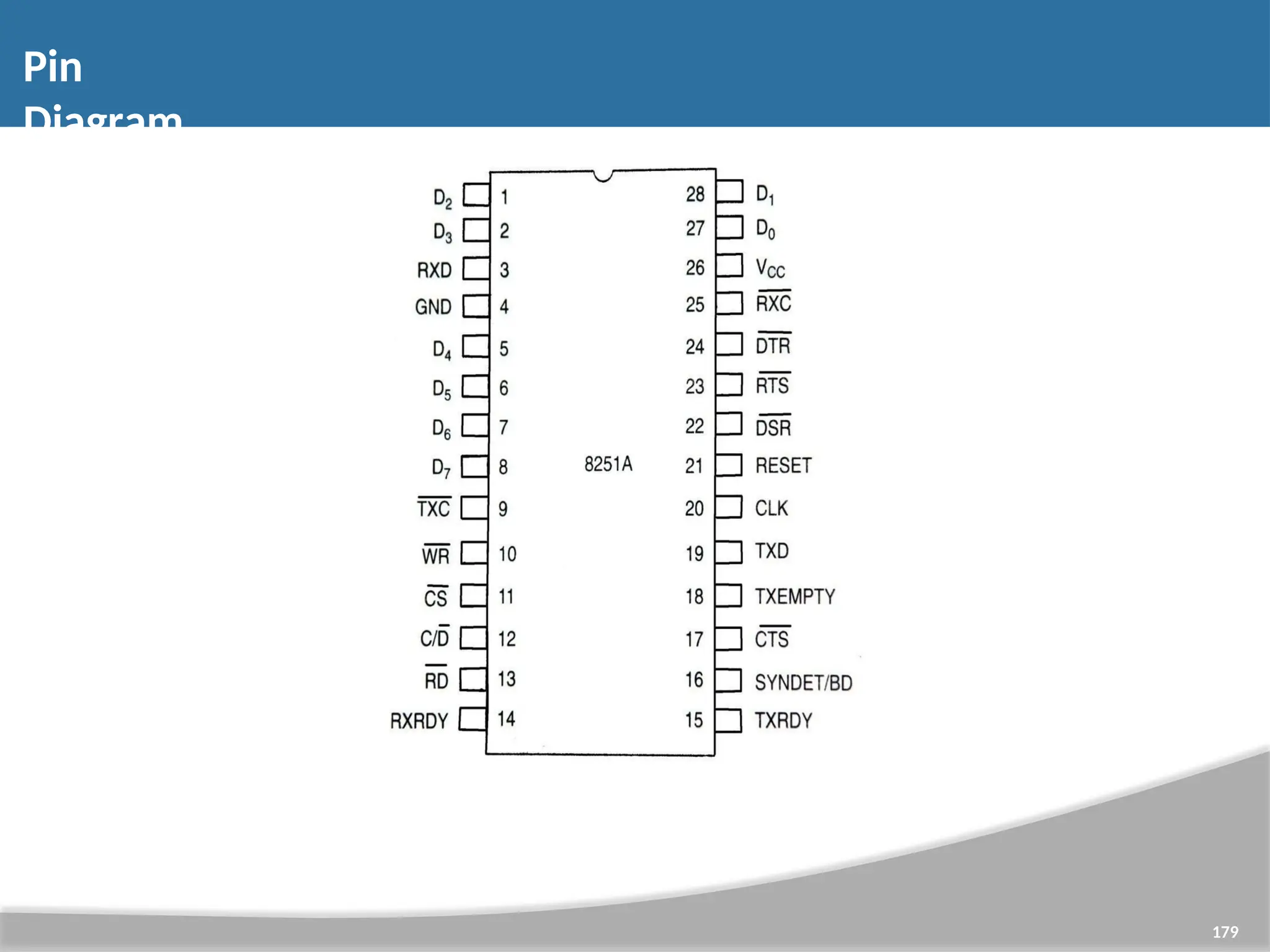
Features 177 Compatible withextended range of Intel microprocessors. It provides both synchronous and asynchronous data transmission. Synchronous 5-8 bit characters. Asynchronous 5-8 bit characters. It has full duplex, double buffered transmitter and receiver. Detects the errors-parity, overrun and framing errors. All inputs and outputs are TTL compatible. Available in 28-pin DIP package.
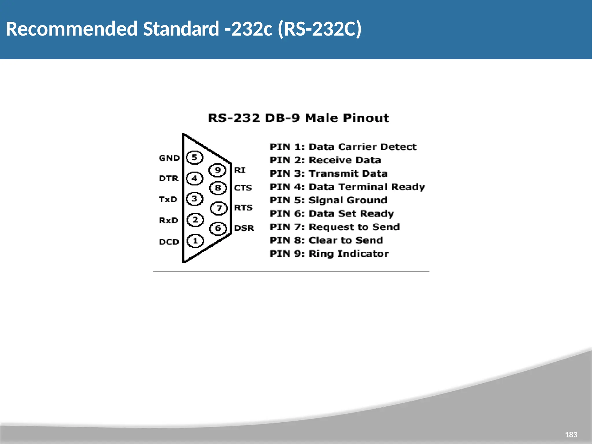
Recommended Standard -232c(RS-232C) 181 • RS-232 was first introduced in 1962 by the Radio Sector of the Electronic Industries Association EIA. RS-232 (Recommended standard-232) is a standard interface approved by the Electronic Industries Association (EIA) for connecting serial devices. In other words, RS-232 is a long-established standard that describes the physical interface and protocol for relatively low-speed serial data communication between computers and related devices. An industry trade group, the Electronic Industries Association (EIA), defined it originally for teletypewriter devices.
182.
Recommended Standard -232c(RS-232C) 182 • In 1987, the EIA released a new version of the standard and changed the name to EIA-232-D. Many people, however, still refer to the standard as RS- 232C, or just RS-232. RS-232 is the interface that your computer uses to talk to and exchange data with your modem and other serial devices. The serial ports on most computers use a subset of the RS- 232C standard.
• Direct memoryaccess (DMA) is a feature of modern computer systems that allows certain hardware subsystems to read/write data to/from memory without microprocessor intervention, allowing the processor to do other work. • Used in disk controllers, video/sound cards etc, or between memory locations. • Typically, the CPU initiates DMA transfer, does other operations while the transfer is in progress, and receives an interrupt from the DMA controller once the operation is complete. • Can create cache coherency problems (the data in the cache may be different from the data in the external memory after DMA) 184 Need For DMA
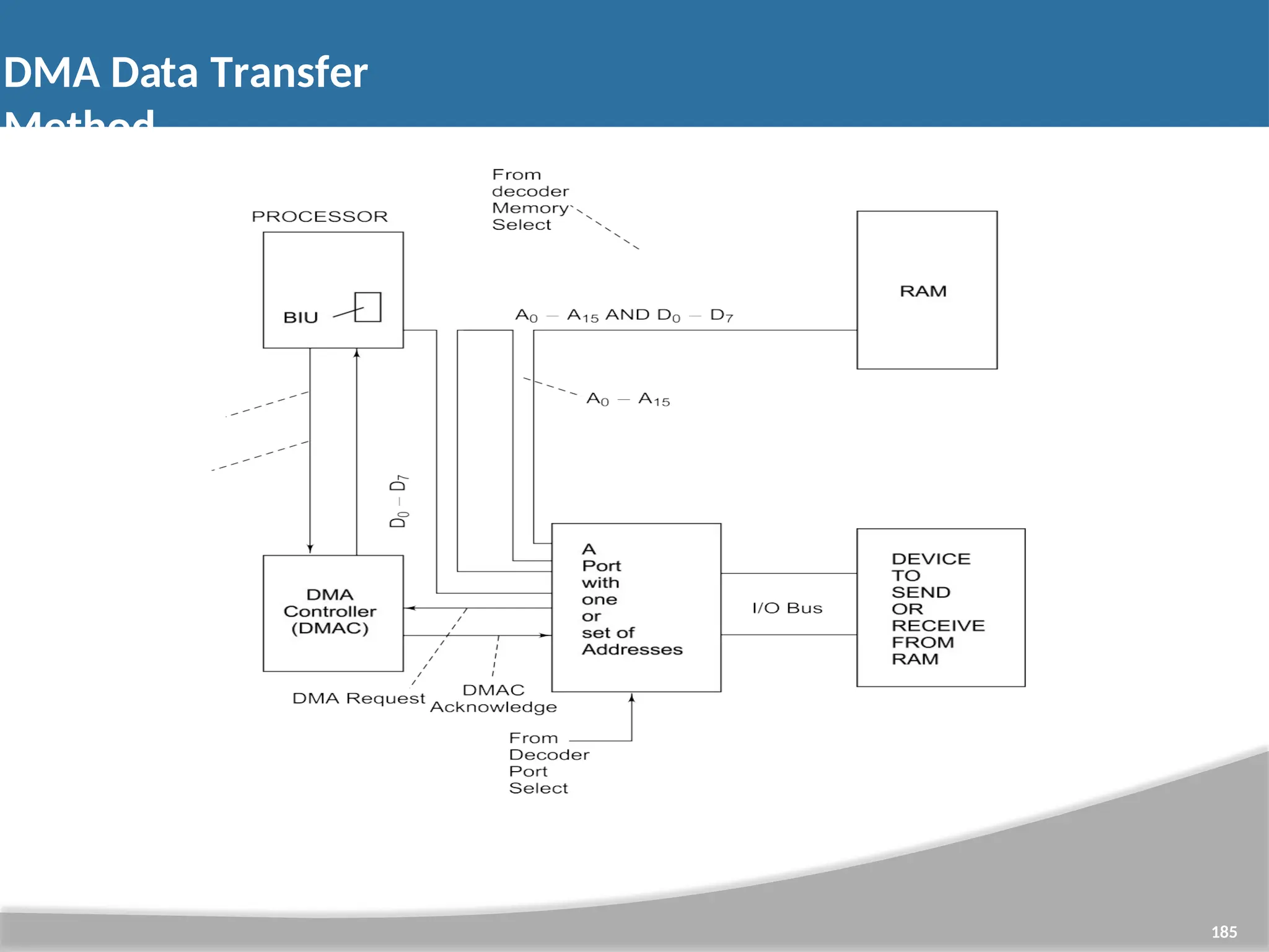
• The I/Odevice asserts the appropriate DRQ signal for the channel. • The DMA controller will enable appropriate channel, and ask the CPU to release the bus so that the DMA may use the bus. The DMA requests the bus by asserting the HOLD signal which goes to the CPU. • The CPU detects the HOLD signal, and will complete executing the current instruction. Now all of the signals normally generated by the CPU are placed in a tri-stated condition (neither high or low) and then the CPU asserts the HLDA signal which tells the DMA controller that it is now in charge of the bus. • The CPU may have to wait (hold cycles). 186 DMA Data Transfer Method
187.
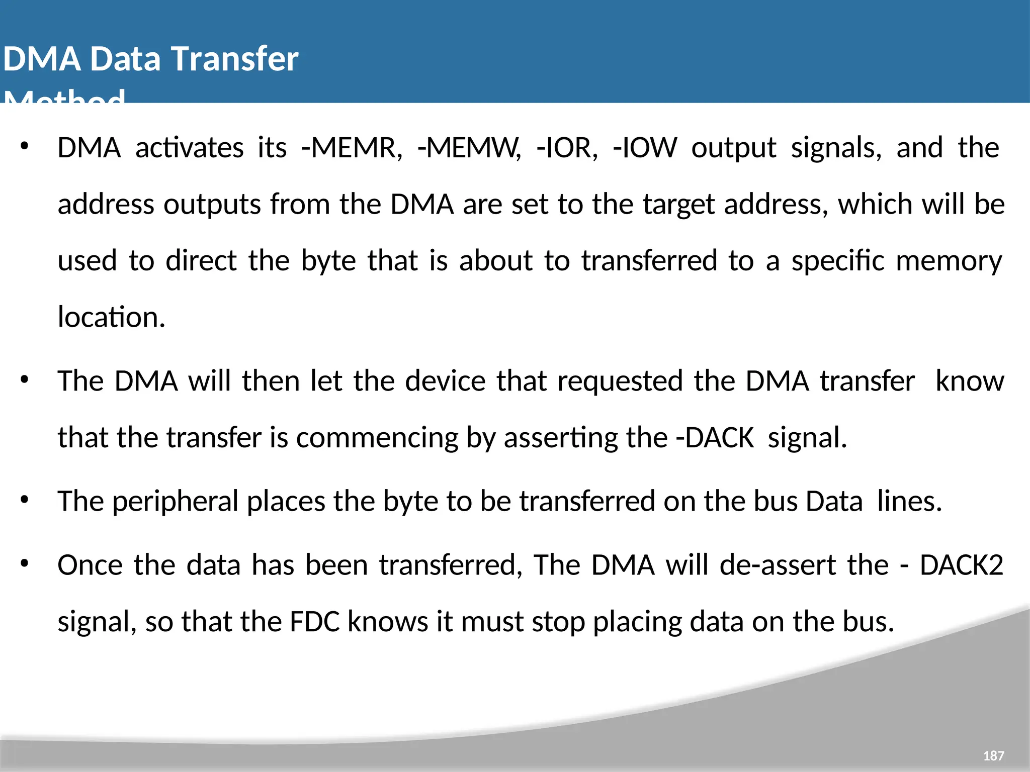
• DMA activatesits -MEMR, -MEMW, -IOR, -IOW output signals, and the address outputs from the DMA are set to the target address, which will be used to direct the byte that is about to transferred to a specific memory location. • The DMA will then let the device that requested the DMA transfer know that the transfer is commencing by asserting the -DACK signal. • The peripheral places the byte to be transferred on the bus Data lines. • Once the data has been transferred, The DMA will de-assert the - DACK2 signal, so that the FDC knows it must stop placing data on the bus. 187 DMA Data Transfer Method
188.
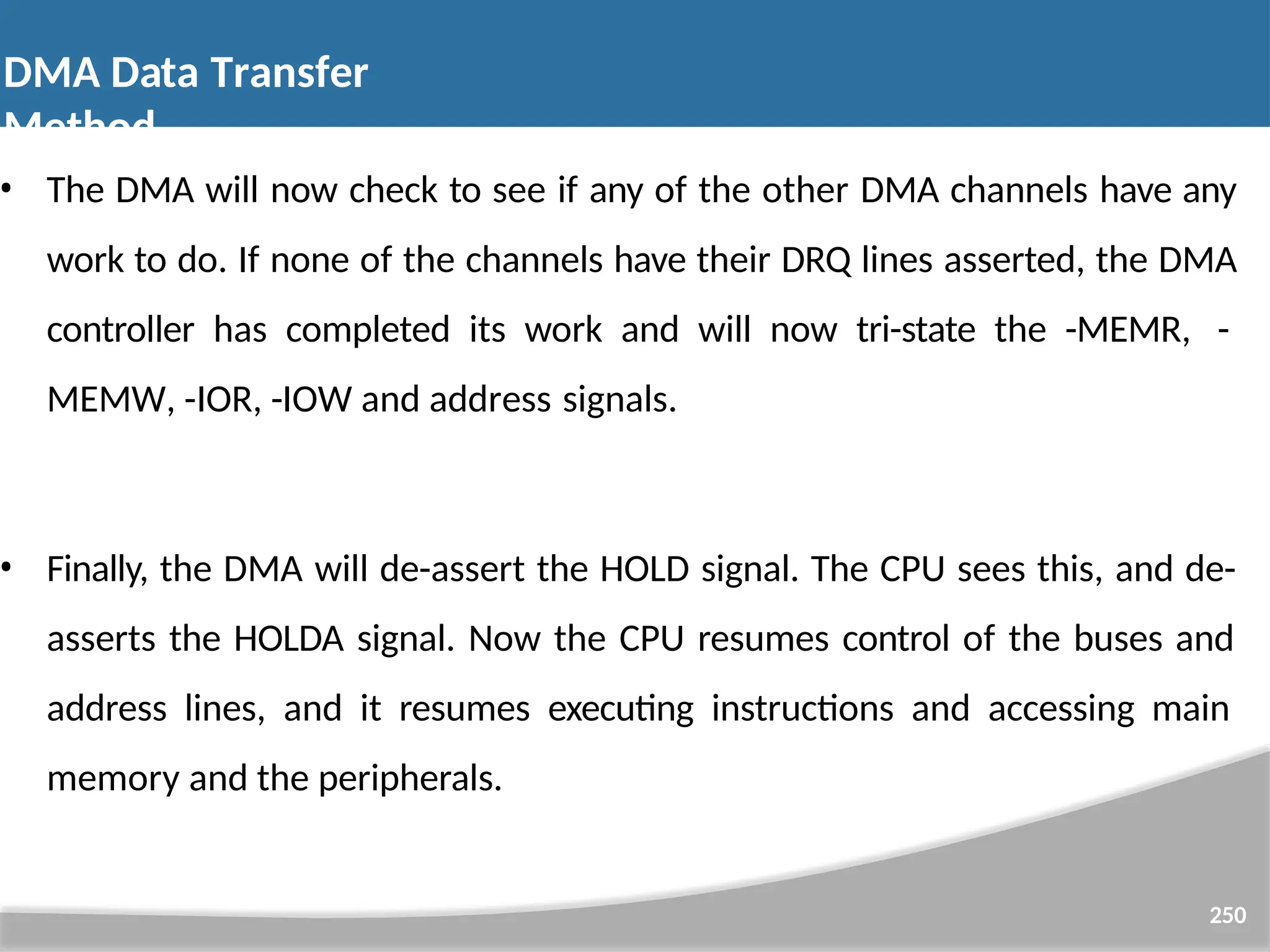
• The DMAwill now check to see if any of the other DMA channels have any work to do. If none of the channels have their DRQ lines asserted, the DMA controller has completed its work and will now tri-state the -MEMR, - MEMW, -IOR, -IOW and address signals. • Finally, the DMA will de-assert the HOLD signal. The CPU sees this, and de- asserts the HOLDA signal. Now the CPU resumes control of the buses and address lines, and it resumes executing instructions and accessing main memory and the peripherals. 250 DMA Data Transfer Method
189.
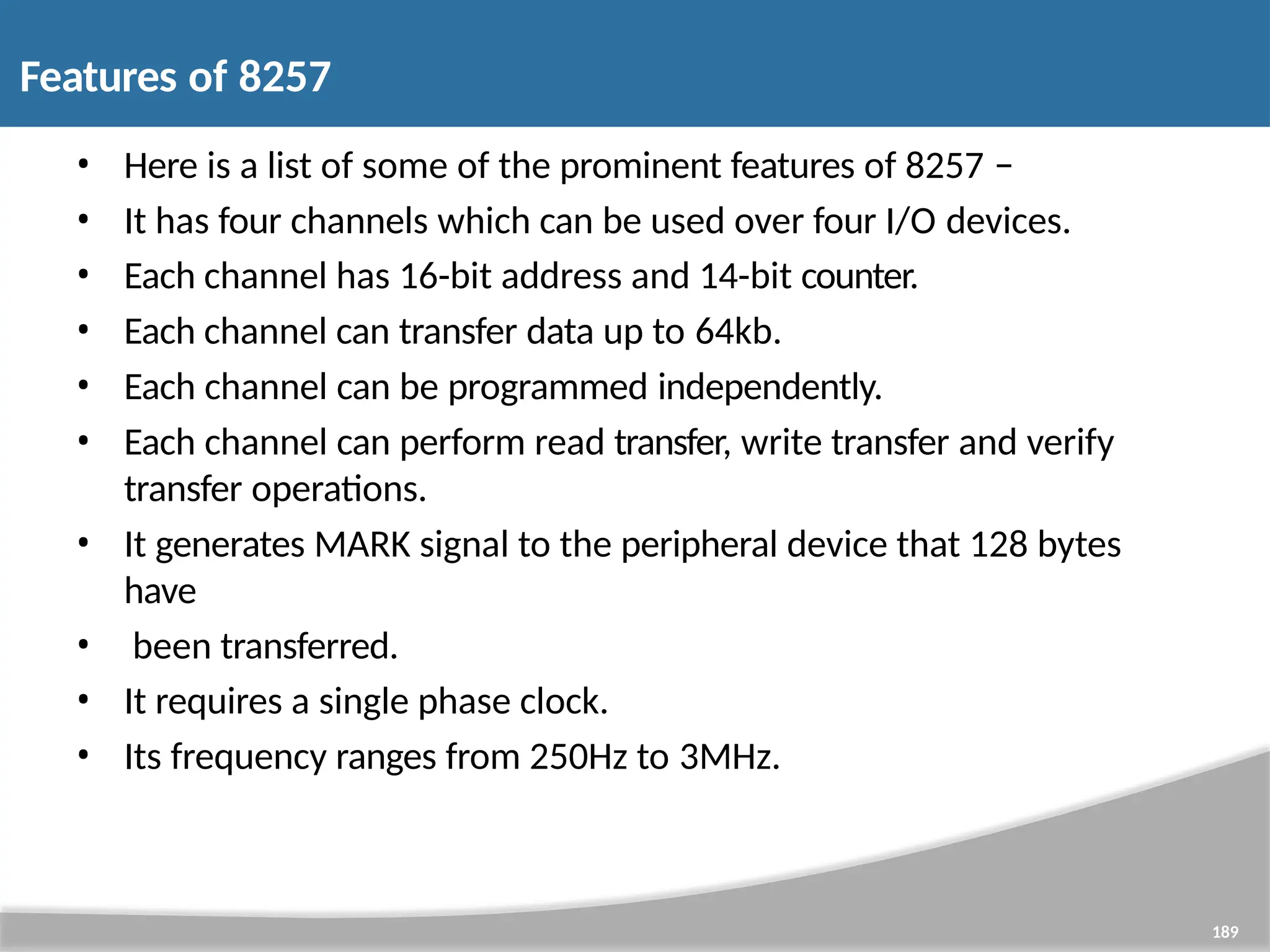
• Here isa list of some of the prominent features of 8257 − • It has four channels which can be used over four I/O devices. • Each channel has 16-bit address and 14-bit counter. • Each channel can transfer data up to 64kb. • Each channel can be programmed independently. • Each channel can perform read transfer, write transfer and verify transfer operations. • It generates MARK signal to the peripheral device that 128 bytes have • been transferred. • It requires a single phase clock. • Its frequency ranges from 250Hz to 3MHz. 189 Features of 8257
The overallsystem cost is high. A large sized PCB is required components. 197 for assembling all the Overall product design requires more time. Physical size of the product is big. A discrete components are used, the system is not reliable. Disadvantages of Microprocessor
198.
As theperipherals are integrated into a single chip, the overall system cost is very less. 198 As the peripherals are integrated with a microprocessor the more reliable. system is Though microcontroller may have on chip ROM,RAM and I/O ports, addition ROM, RAM I/O ports may be interfaced externally if required. On chip ROM provide a software security. Advantages of Microcontroller based System
199.
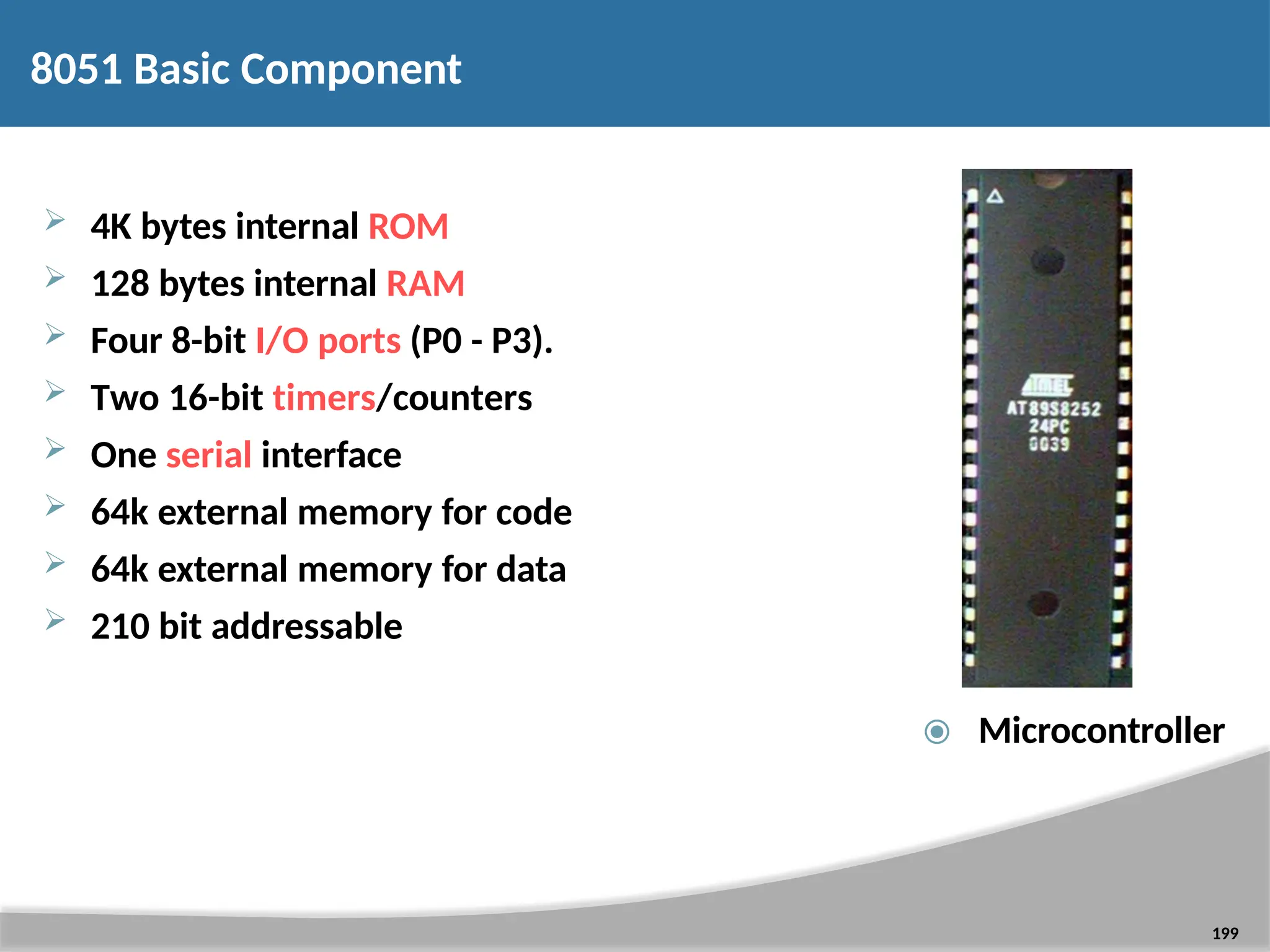
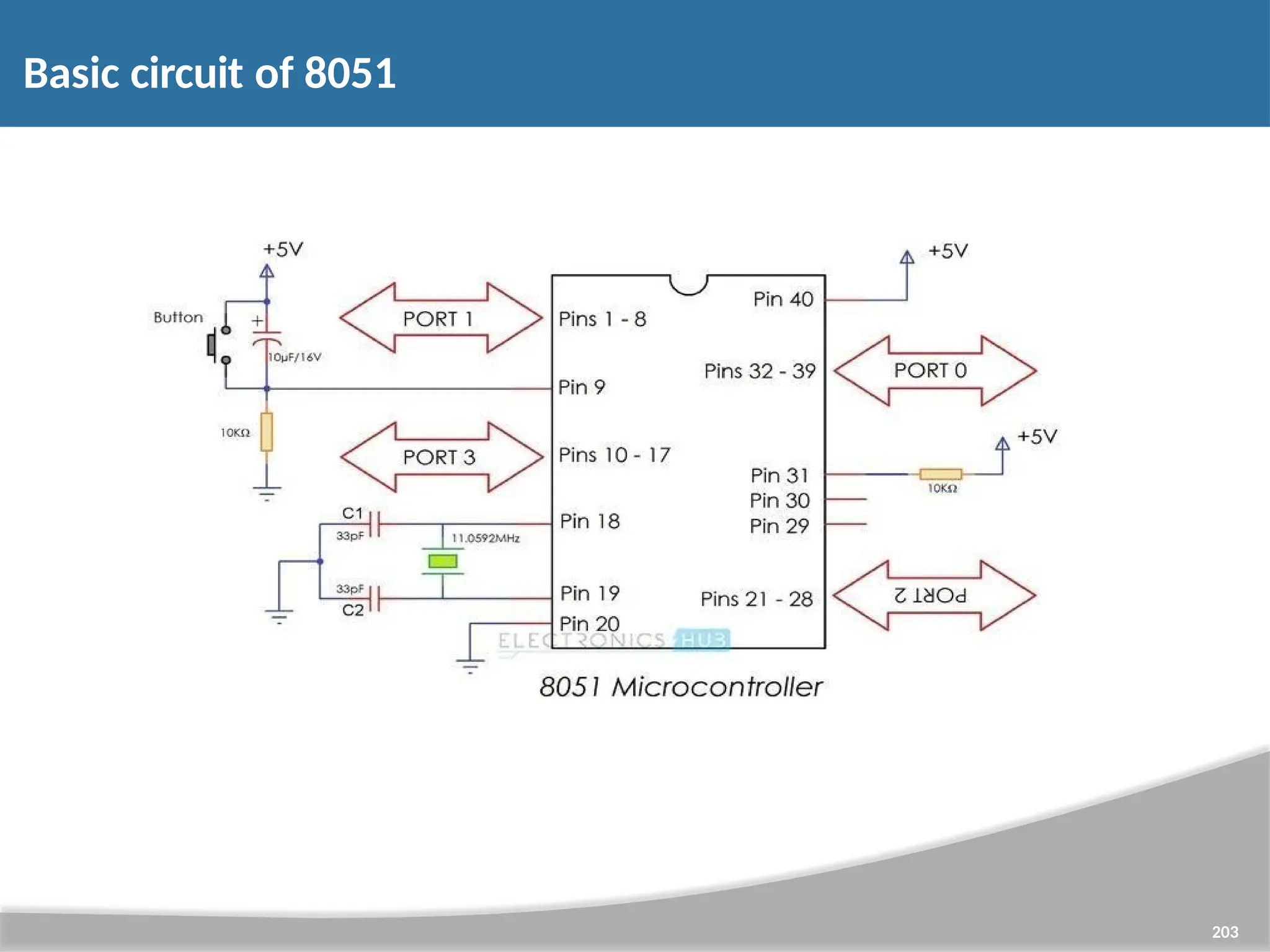
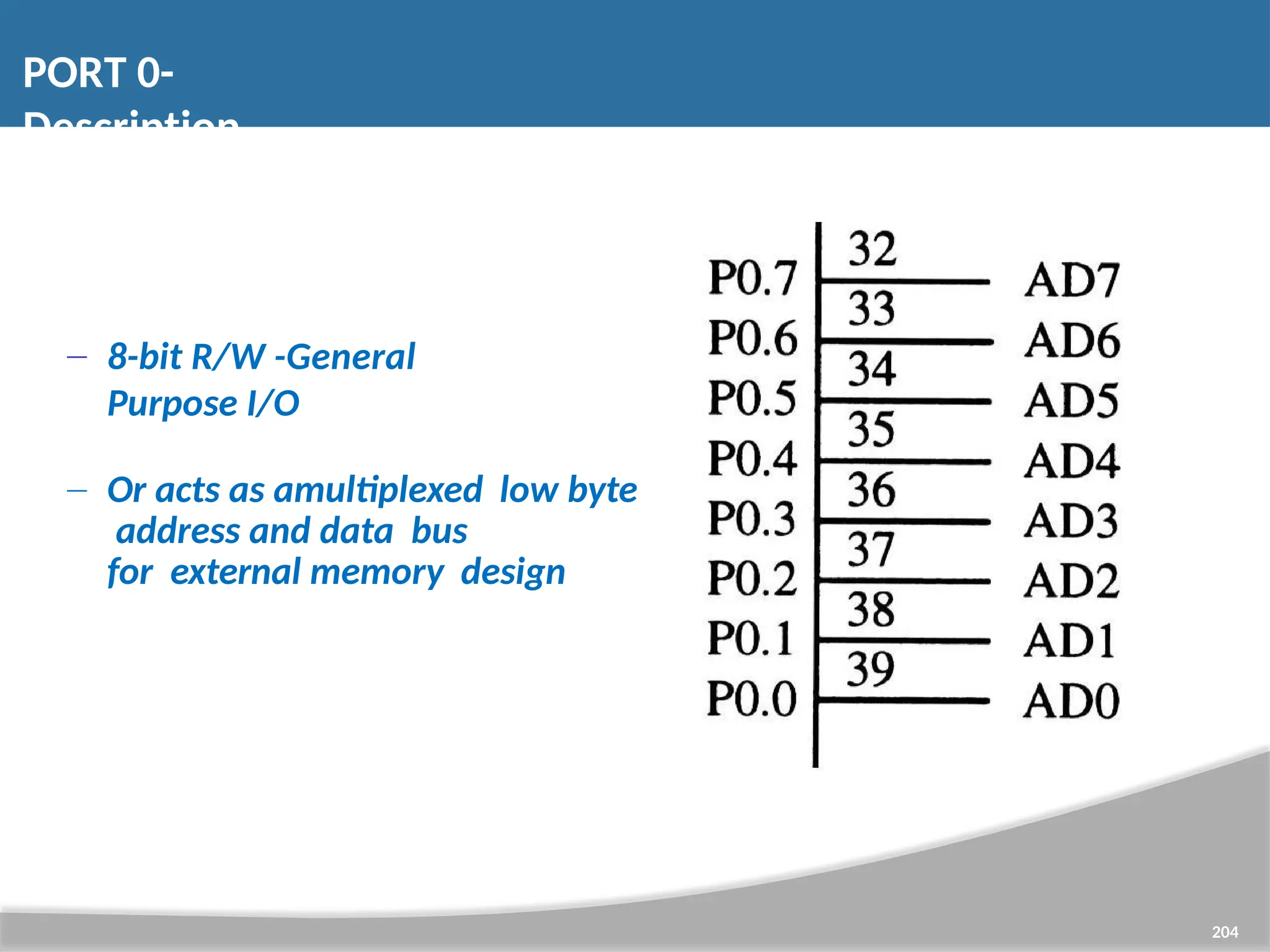
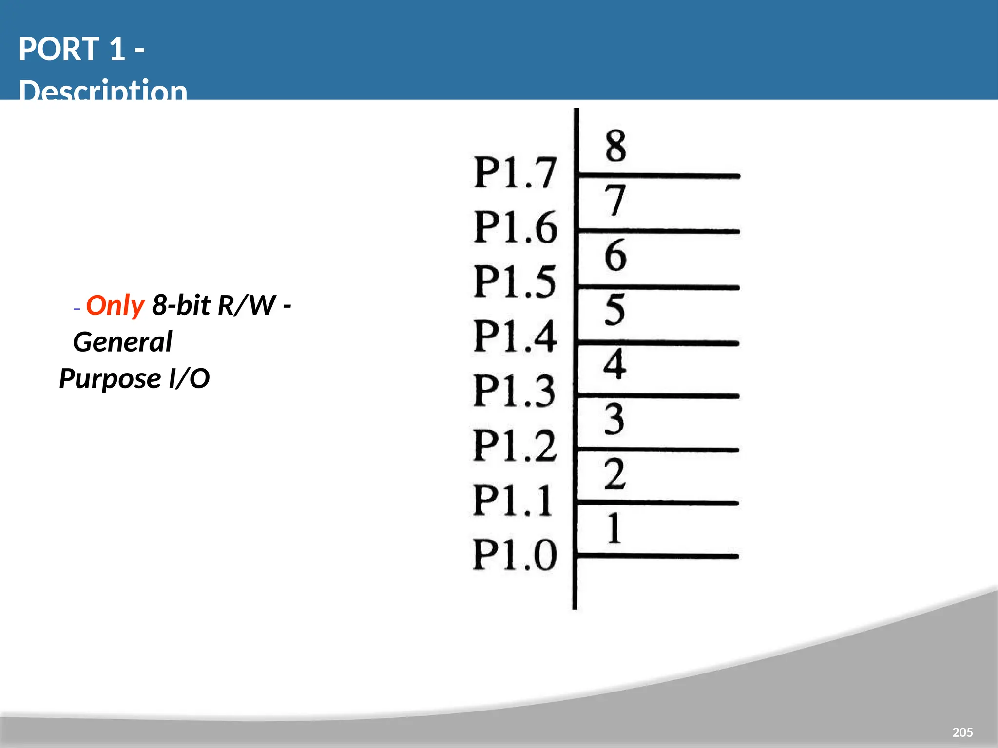
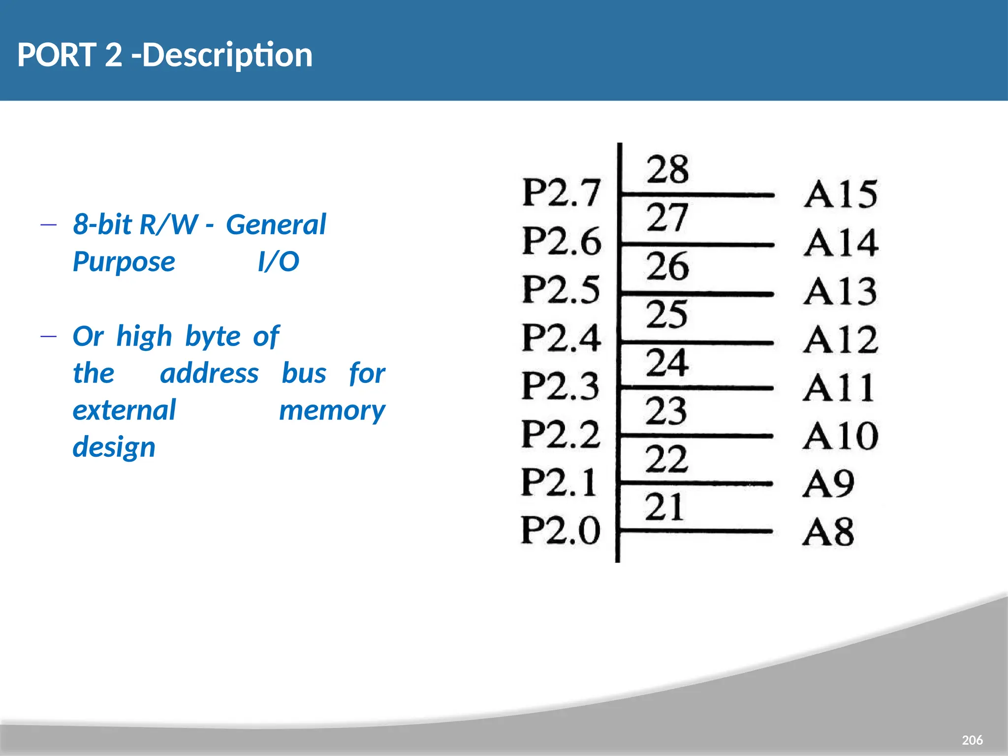
8051 Basic Component 4K bytes internal ROM 128 bytes internal RAM Four 8-bit I/O ports (P0 - P3). Two 16-bit timers/counters One serial interface 64k external memory for code 64k external memory for data 210 bit addressable ⦿ Microcontroller 199
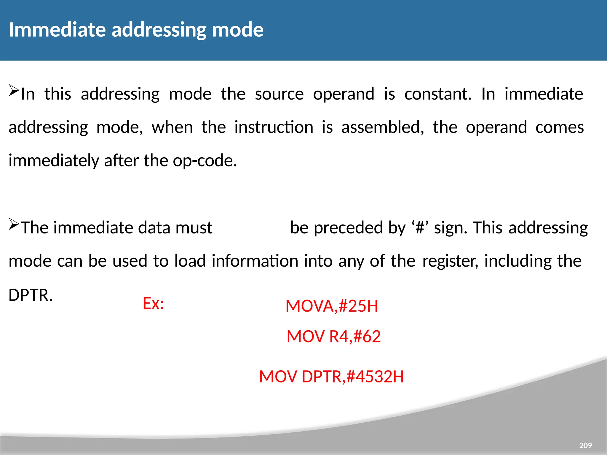
Immediate addressing mode 209 Inthis addressing mode the source operand is constant. In immediate addressing mode, when the instruction is assembled, the operand comes immediately after the op-code. The immediate data must be preceded by ‘#’ sign. This addressing mode can be used to load information into any of the register, including the DPTR. Ex: MOVA,#25H MOV R4,#62 MOV DPTR,#4532H
210.
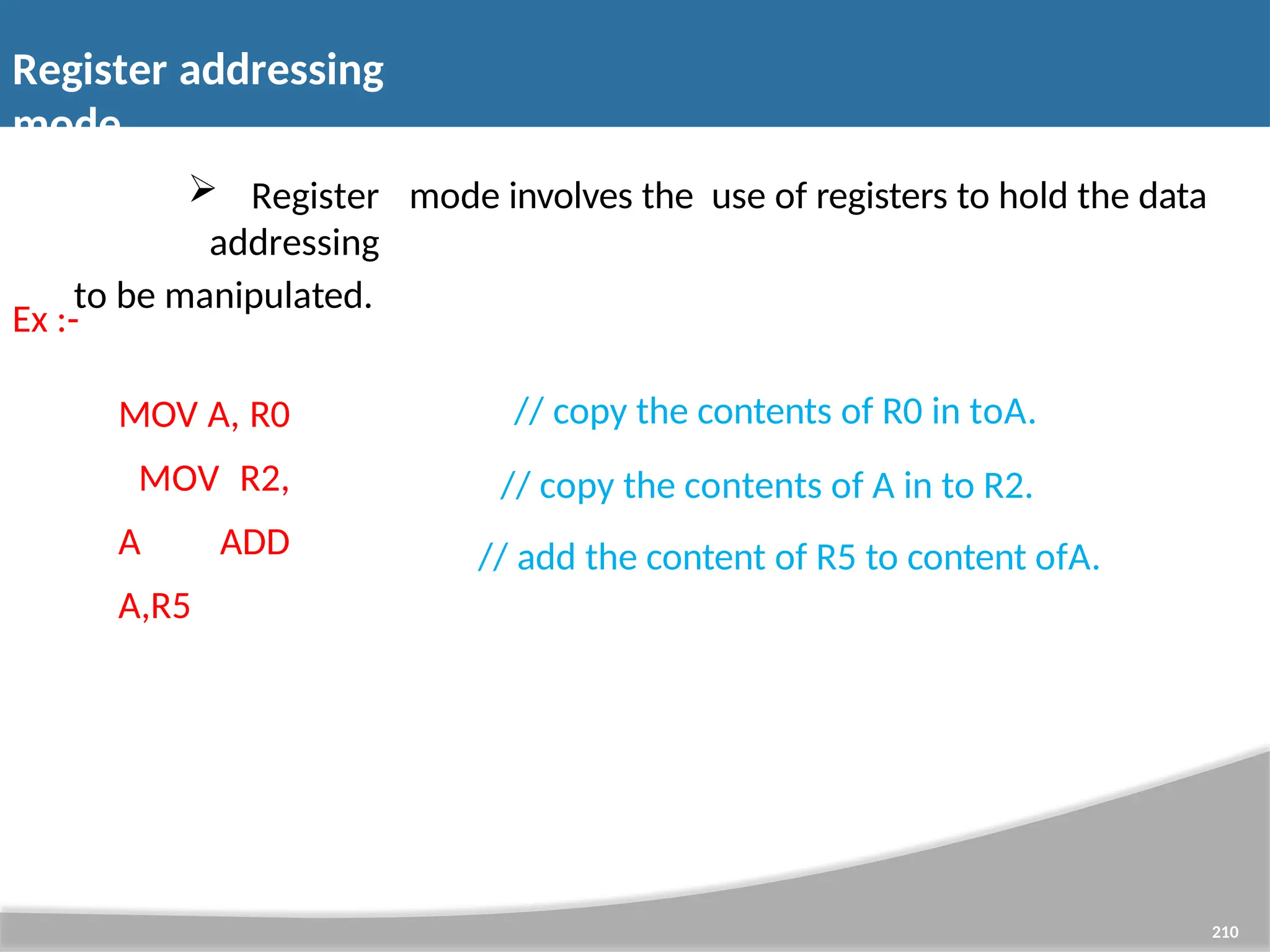
Register addressing mode 210 Register addressing tobe manipulated. mode involves the use of registers to hold the data Ex :- MOV A, R0 MOV R2, A ADD A,R5 // copy the contents of R0 in toA. // copy the contents of A in to R2. // add the content of R5 to content ofA.
211.
Direct addressing mode 211 Indirect addressing mode, the data is in a RAM memory location whose address is known, and this address is given as a part of the instruction. Contrast this with the immediate addressing mode in which itself is provided with the instruction. Ex:- the operand MOV R0,40H //save content of RAM location 40h into R0. MOV 56H,A // save content of A in RAM location 56H
212.
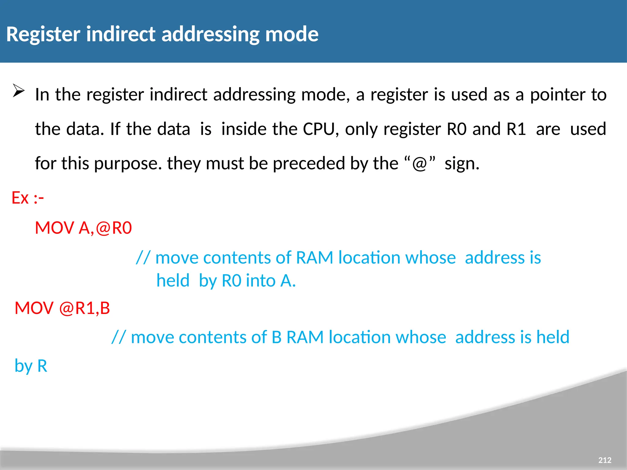
Register indirect addressingmode 212 In the register indirect addressing mode, a register is used as a pointer to the data. If the data is inside the CPU, only register R0 and R1 are used for this purpose. they must be preceded by the “@” sign. Ex :- MOV A,@R0 // move contents of RAM location whose address is held by R0 into A. MOV @R1,B // move contents of B RAM location whose address is held by R
213.
Indexed addressing mode 213 Indexedaddressing mode is widely used in accessing data elements of look- up table entries located in the program ROM space of the 8051. The instruction used for this purpose is “MOV A, @A+DPTR”. Indexed addressing mode is widely used in accessing data elements of look- up table entries located in the program ROM space of the 8051. The instruction used for this purpose is “MOV A, @A+DPTR”.
214.
Instruction set of8051 8051 has simple instruction set in different groups. There are, Arithmeticinstructions Logicalinstructions Data transferinstructions Branching and loopinginstructions Bit controlinstructions 214
215.
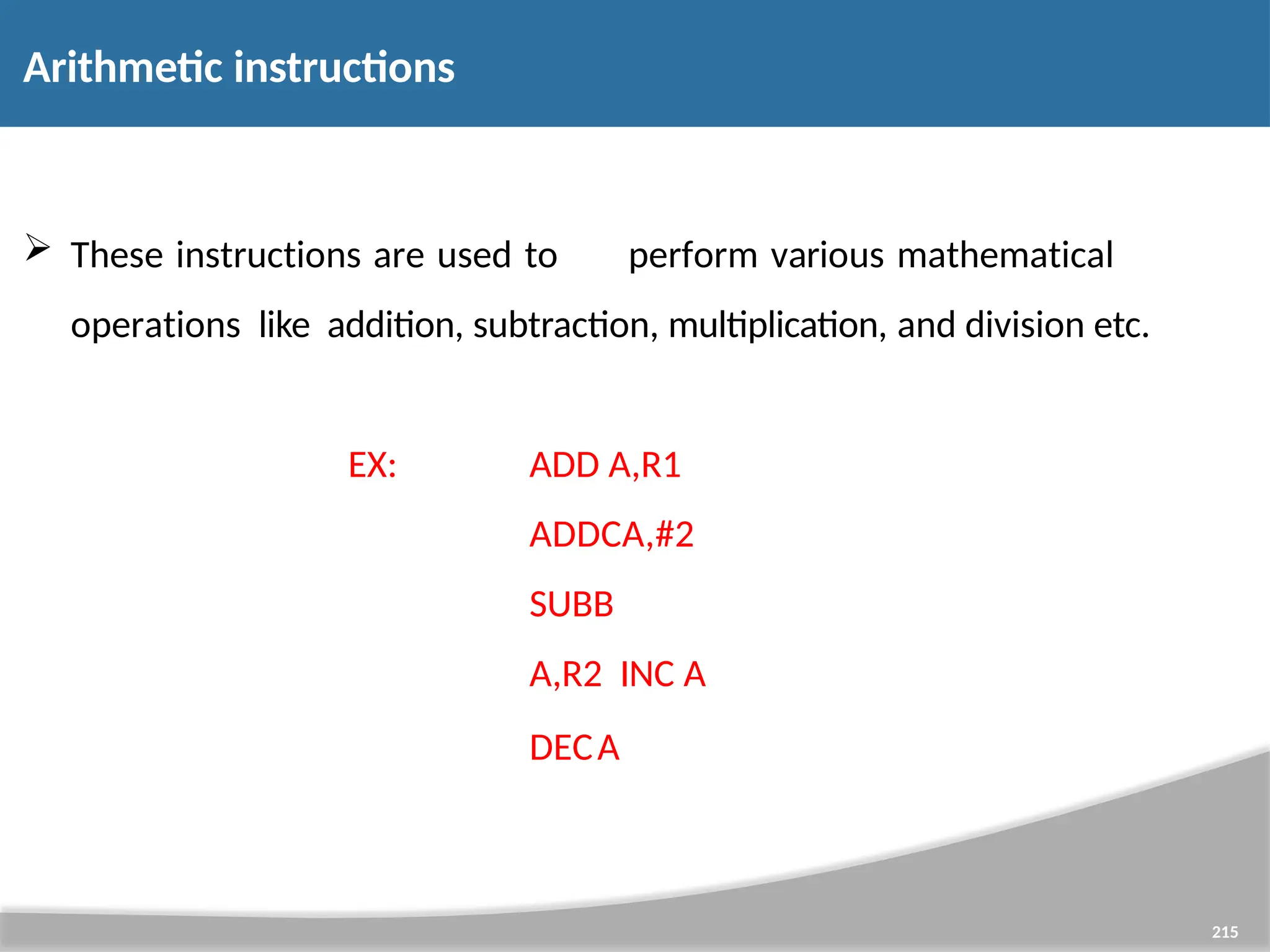
Arithmetic instructions 215 Theseinstructions are used to perform various mathematical operations like addition, subtraction, multiplication, and division etc. EX: ADD A,R1 ADDCA,#2 SUBB A,R2 INC A DECA
216.
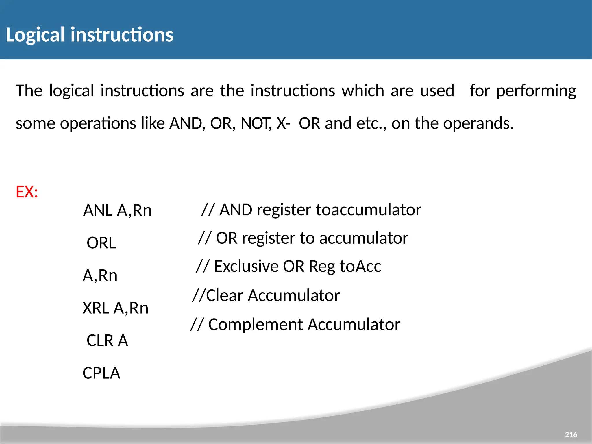
Logical instructions 216 The logicalinstructions are the instructions which are used for performing some operations like AND, OR, NOT, X- OR and etc., on the operands. EX: ANL A,Rn ORL A,Rn XRL A,Rn CLR A CPLA // AND register toaccumulator // OR register to accumulator // Exclusive OR Reg toAcc //Clear Accumulator // Complement Accumulator
217.
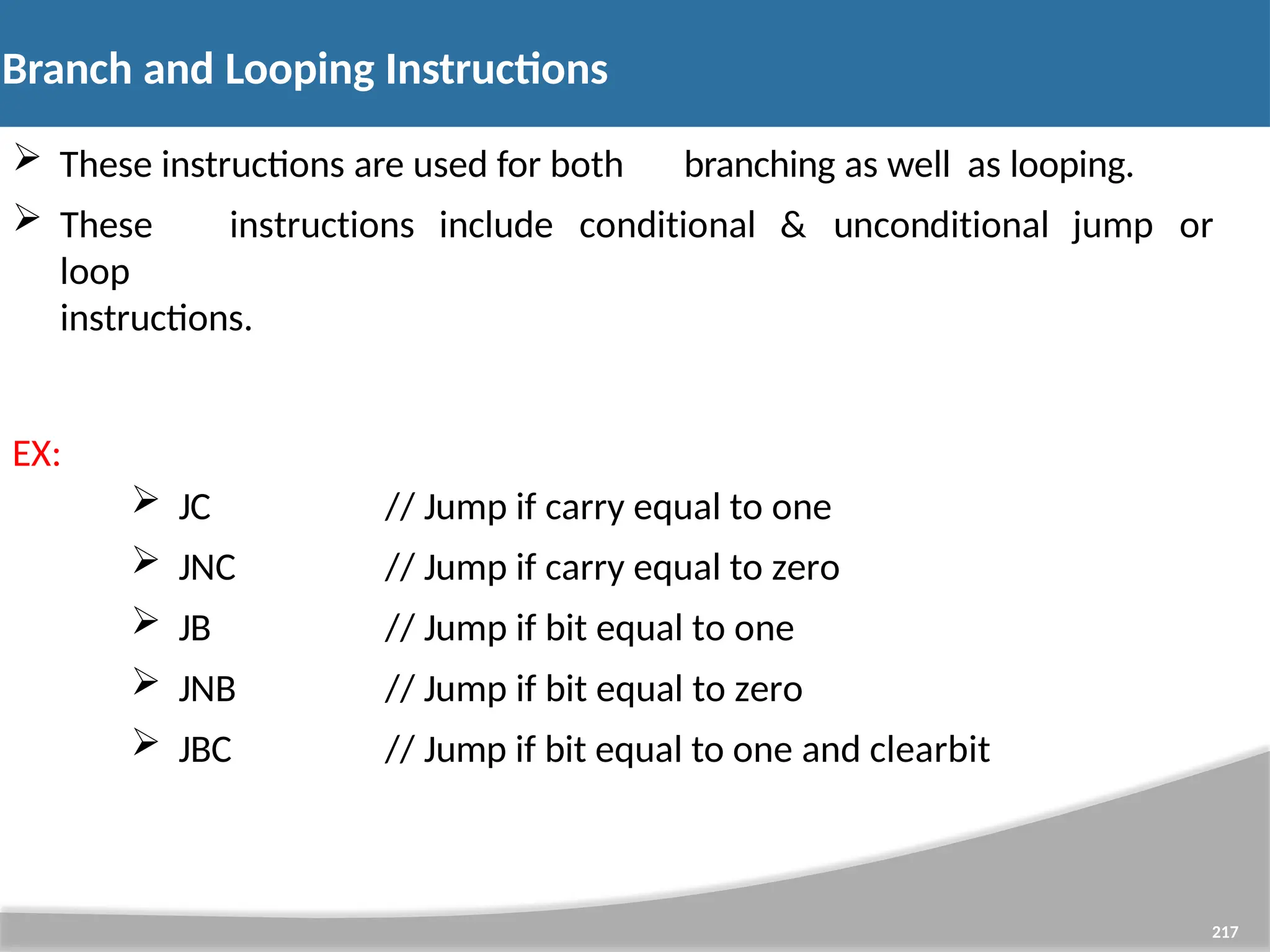
Branch and LoopingInstructions 217 These instructions are used for both branching as well as looping. These instructions include conditional & unconditional jump or loop instructions. EX: JC JNC JB JNB JBC // Jump if carry equal to one // Jump if carry equal to zero // Jump if bit equal to one // Jump if bit equal to zero // Jump if bit equal to one and clearbit
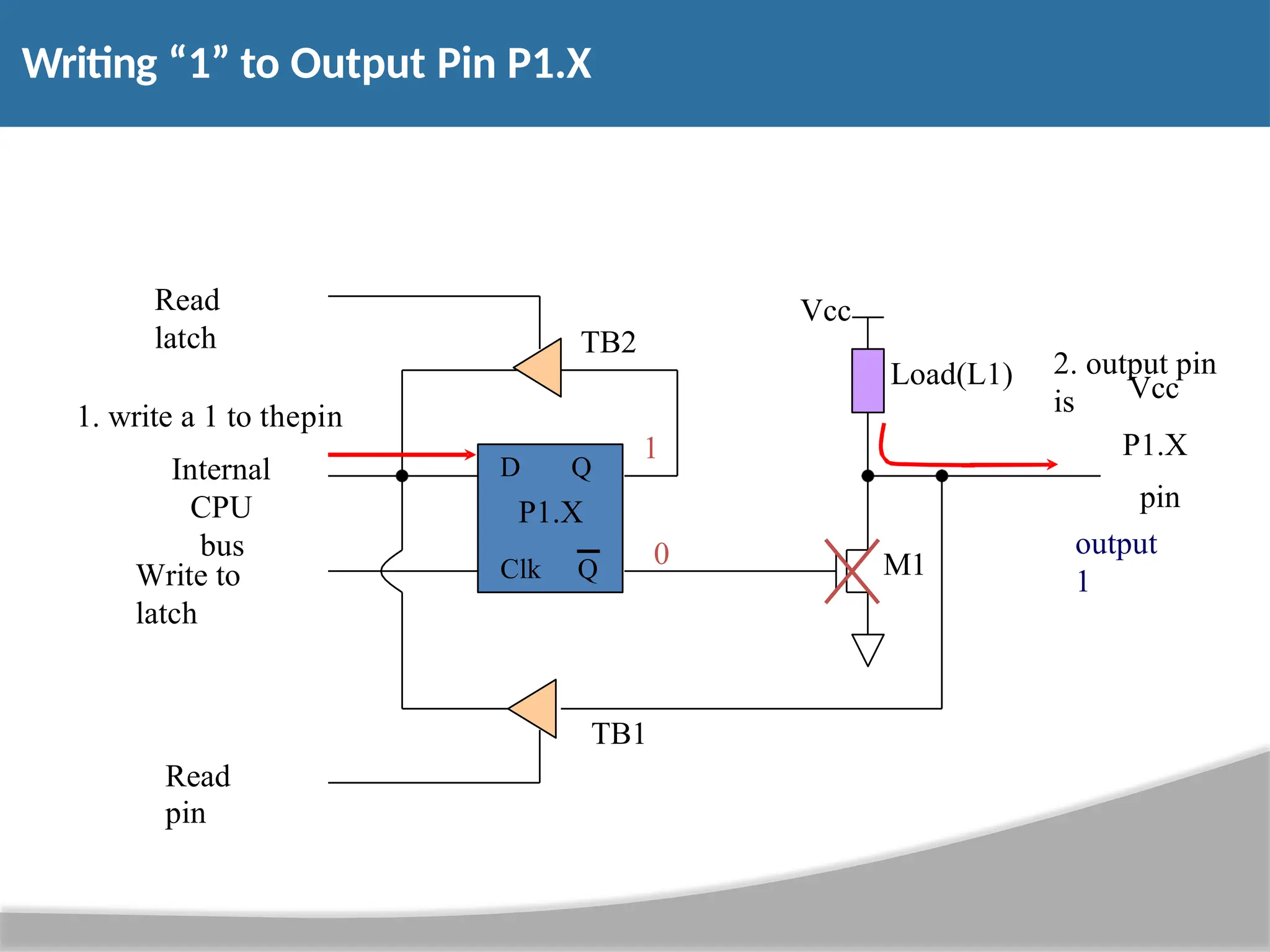
Writing “1” toOutput Pin P1.X Vcc Load(L1) Read latch Write to latch Internal CPU bus M1 D Q P1.X Clk Q 2. output pin is Vcc P1.X pin 1. write a 1 to thepin 1 TB1 Read pin 0 output 1 TB2
220.
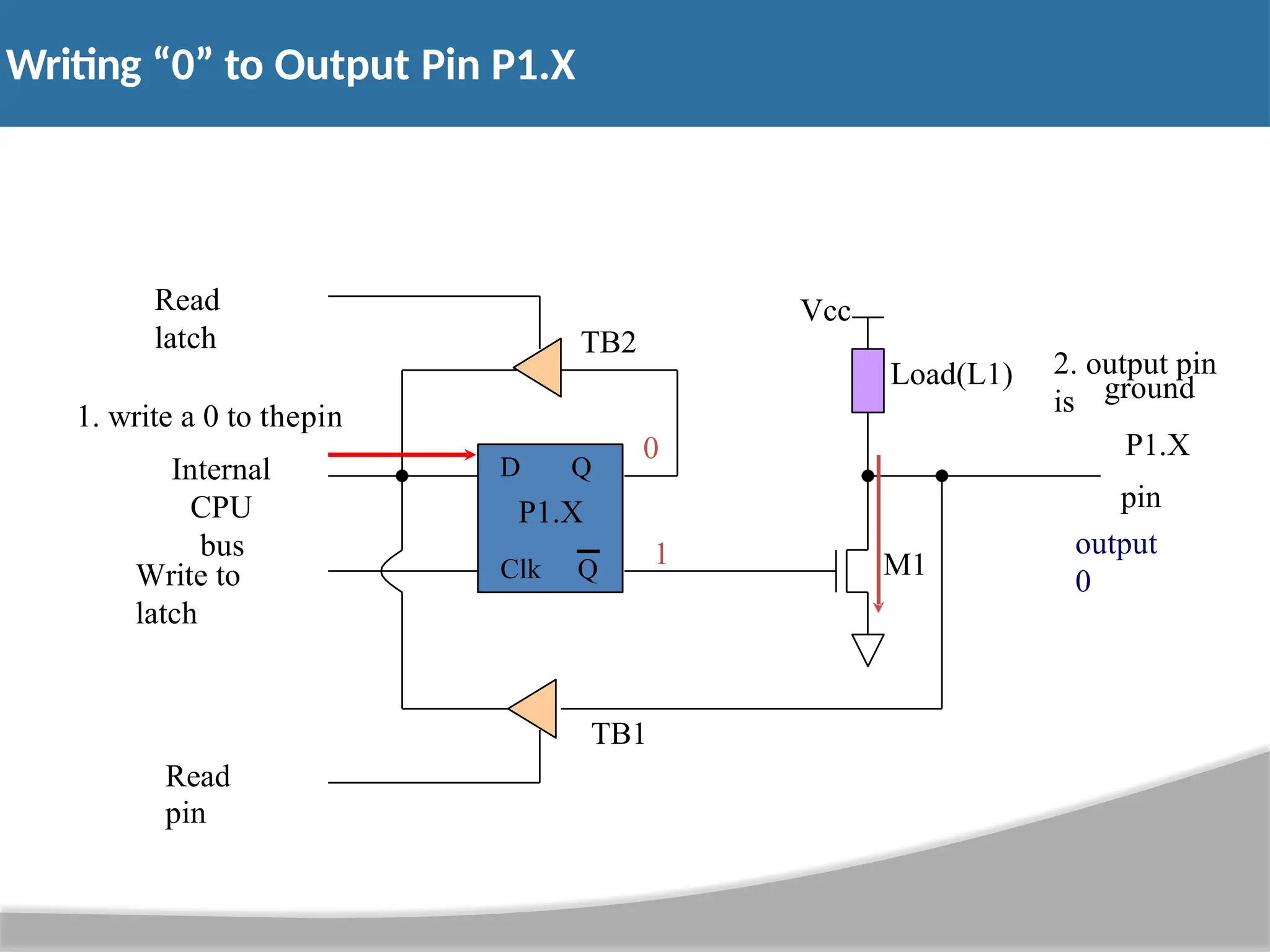
Writing “0” toOutput Pin P1.X Vcc Load(L1) Read latch Write to latch Internal CPU bus M1 D Q P1.X Clk Q 2. output pin is ground P1.X pin 1. write a 0 to thepin 0 TB1 Read pin 1 output 0 TB2
221.
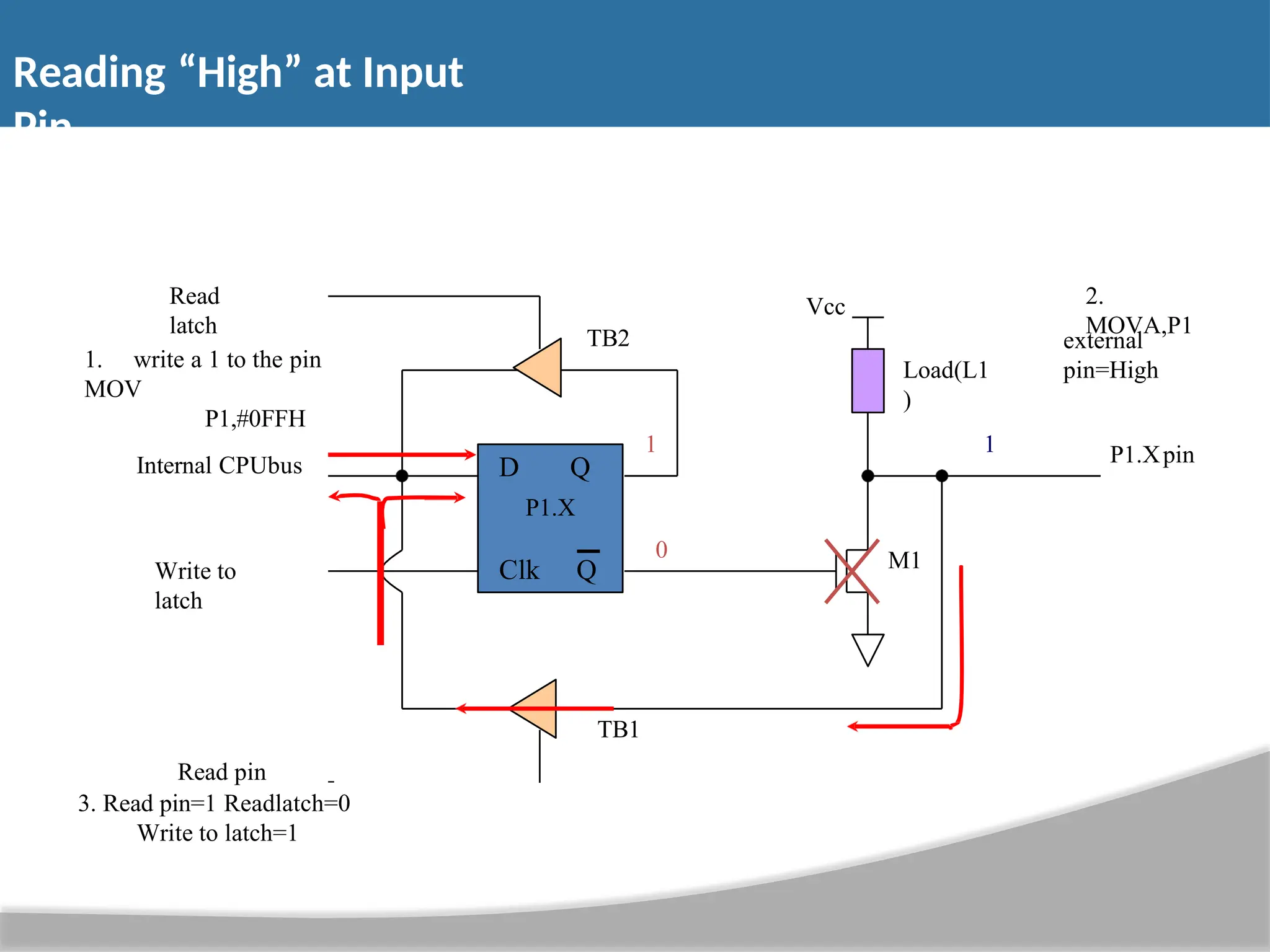
Reading “High” atInput Pin Vcc Load(L1 ) Read latch Write to latch Internal CPUbus M1 P1.Xpin D Q P1.X Clk Q 2. MOVA,P1 TB1 Read pin 3. Read pin=1 Readlatch=0 Write to latch=1 external pin=High 1. write a 1 to the pin MOV P1,#0FFH 1 0 1 TB2
222.
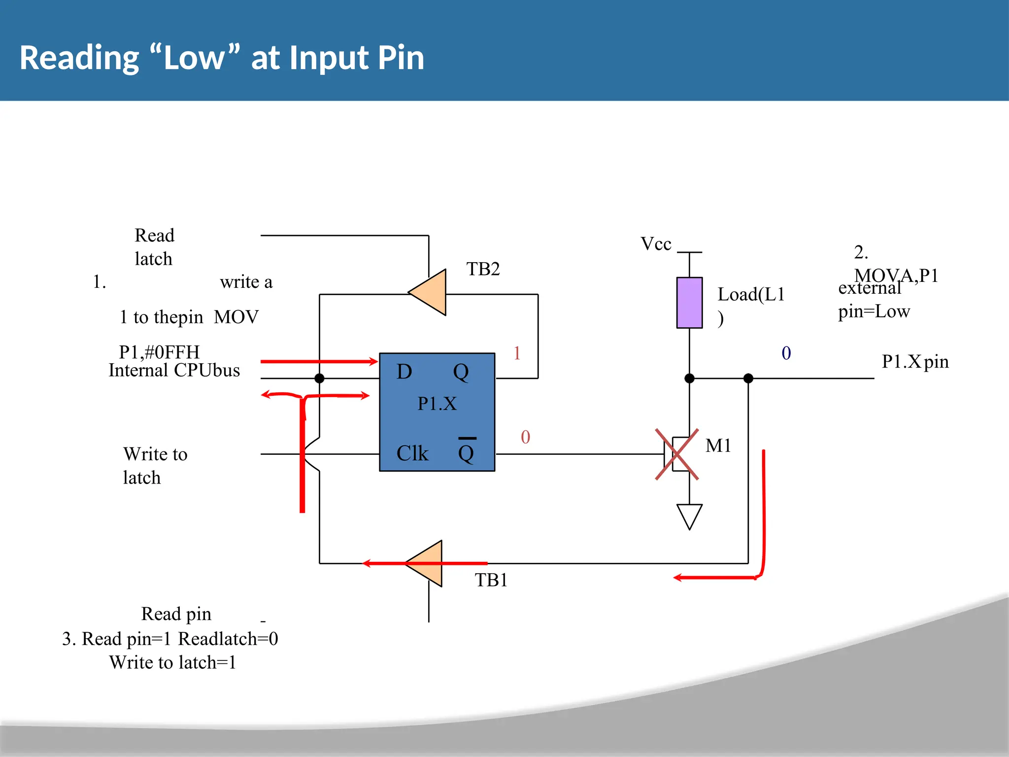
Reading “Low” atInput Pin Vcc Load(L1 ) Read latch Write to latch Internal CPUbus M1 P1.Xpin D Q P1.X Clk Q 2. MOVA,P1 TB1 Read pin 3. Read pin=1 Readlatch=0 Write to latch=1 external pin=Low 1. write a 1 to thepin MOV P1,#0FFH 1 0 0 TB2
223.
A and BRegisters • A and B are “accumulators” forarithmetic instructions • They can be accessed by direct mode as special function registers: • B – address 0F0h • A – address 0E0h - use “ACC” for direct mode
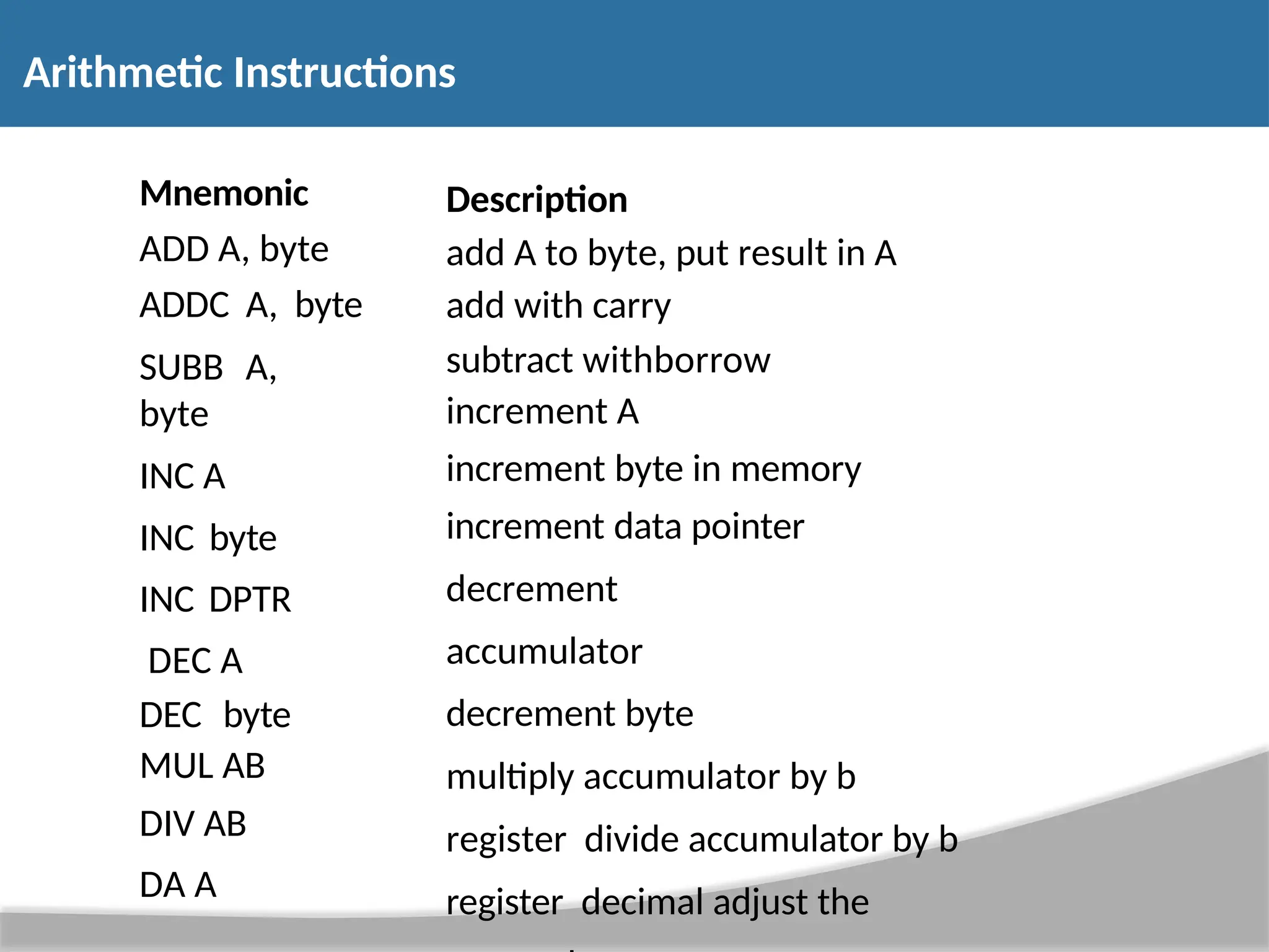
Arithmetic Instructions Mnemonic ADD A,byte ADDC A, byte SUBB A, byte INC A INC byte INC DPTR DEC A DEC byte MUL AB DIV AB DA A Description add A to byte, put result in A add with carry subtract withborrow increment A increment byte in memory increment data pointer decrement accumulator decrement byte multiply accumulator by b register divide accumulator by b register decimal adjust the
226.
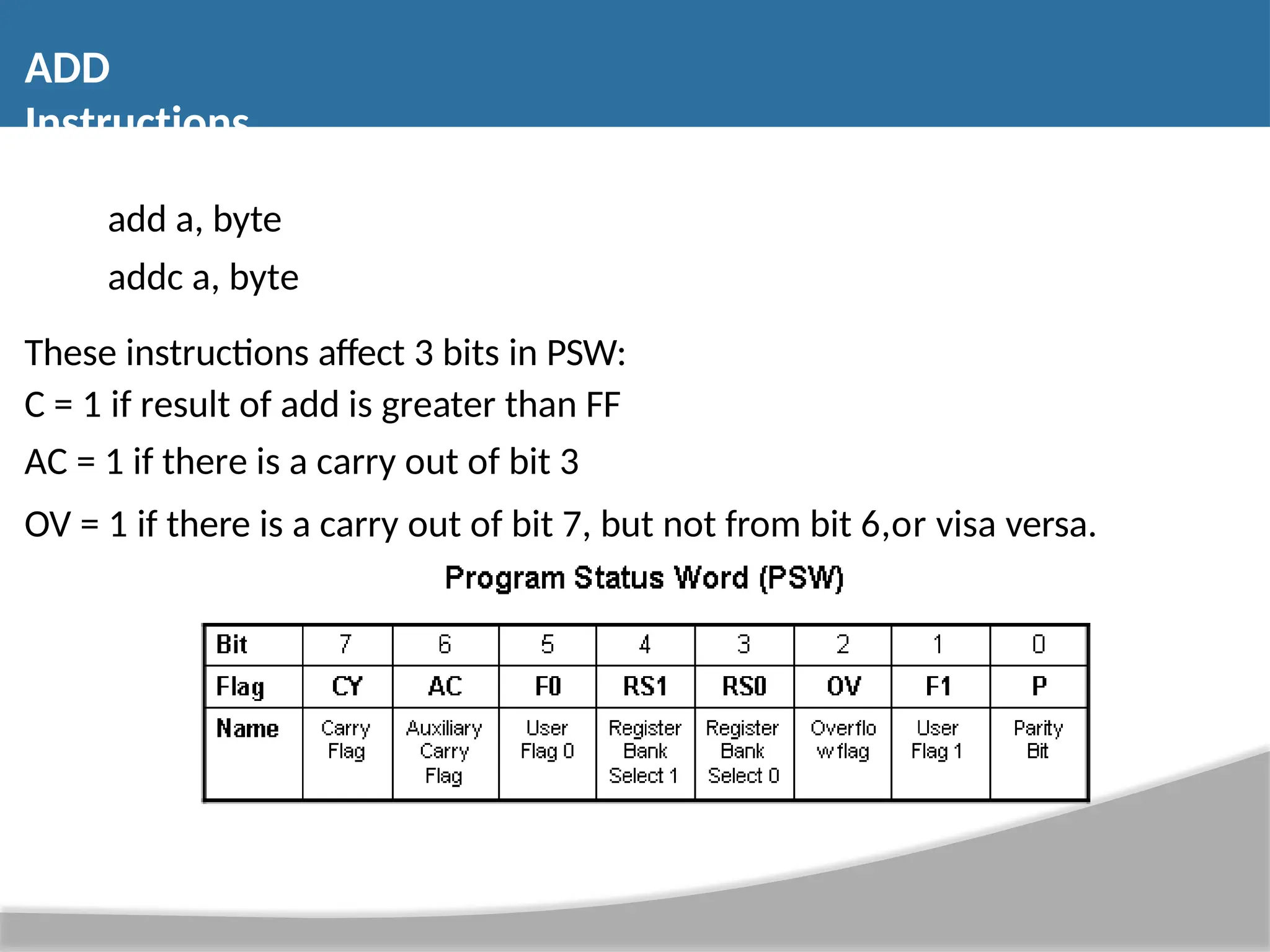
ADD Instructions add a, byte addca, byte These instructions affect 3 bits in PSW: C = 1 if result of add is greater than FF AC = 1 if there is a carry out of bit 3 OV = 1 if there is a carry out of bit 7, but not from bit 6,or visa versa.
227.
Increment and Decrement •The increment and decrement instructions do NOT affect the C flag. • Notice we can only Increment the data pointer, not decrement. INC A increment A INC byte increment byte in memory INC DPTR increment data pointer DEC A decrement accumulator DEC byte decrement byte
228.
Other LogicInstructions • CLR- clear • RL – rotateleft • RLC – rotate left through Carry • RR – rotate right • RRC – rotate right through Carry • SWAP – swap accumulator nibbles
8051 hastwo 16-bit programmable timers/counters. They can be configured to operate either as timers or as event counters. The names of the two counters are T0 and T1 respectively. The timer content is available in four 8-bit special function registers, viz, TL0,TH0,TL1 and TH1 respectively. In the"timer" function mode, the counter is incremented in every machine cycle. Thus, one can think of it as counting machinecycles. Hence the clock rate is 1/12 th of the oscillatorfrequency. In the "counter" function mode, the register is incremented in response to a 1 to 0 transition at its corresponding external input pin (T0 or T1). It requires 2 machine cycles to detect a high to low. TIMER/COUNTER
231.
The operationof the timers/counters is controlled by two special function registers, TMOD and TCON respectively. Timer Mode control (TMOD) Special Function Register: TMOD register is not bit addressable. TMOD Address: 89 H Operation of Timer/Counter
Timer modes ofoperation Timer Mode-0: In this mode, the timer is used as a 13-bit UP counter as follows. Fig: Operation of Timer in Mode 2 The lower 5 bits of TLX and 8 bits of THX are used for the 13 bit count. Upper 3 bits of TLX are ignored. When the counter rolls over from all 0's to all 1's, TFX flag is set and an interrupt is generated.
234.
Timer modes ofoperation The input pulse is obtained from the previous stage. If TR1/0 bit is 1 and Gate bit is 0, the counter continues counting up. If TR1/0 bit is 1 and Gate bit is 1, then the operation of the counter is controlled by input. This mode is useful to measure the width of a given pulse fed to input.
235.
This modeis similar to mode-0 except for the fact that the Timer operates in 16-bit mode. Timer Mode- 1: Fig: Operation of Timer in Mode 1
236.
Timer Mode-2: (Auto-ReloadMode) This is a 8 bit counter/timer operation. Counting is performed in TLX while THX stores a constant value. In this mode when the timer overflows i.e. TLX becomes FFH, it is fed with the value stored in THX. For example if we load THX with 50H then the timer in mode 2 will count from 50H to FFH. After that 50H is again reloaded. This mode is useful in applications like fixed time sampling Fig: Operation of Timer in Mode 2
237.
Timer Mode- 3: Timer 1in mode-3 simply holds its count. The effect is same as setting TR1=0. Timer0 in mode-3 establishes TL0 and TH0 as two separate counters. Fig: Operation of Timer in Mode 3 Control bits TR1 and TF1 are used by Timer-0 (higher 8 bits) (TH0) in Mode-3 while TR0 and TF0 are available to Timer-0 lower 8 bits(TL0).
238.
An interruptis an external or internal event that microcontroller to inform it that a device needs its service. interrupts the Interrupts vs. Polling A single microcontroller can serve several devices. There are two ways to do that: – interrupts – polling. Interrupts
239.
In Polling, the microcontroller ‘s program simply checks each of the I/O devices to see if any device needs servicing. If so, it performs the service. In the interrupt method, whenever any device needs microcontrollers service, it tells to microcontroller by sending an interrupt signal. The program which is associated with the interrupt is called the interrupt service routine (ISR) or interrupt handler. Interrupts
240.
Finish currentinstruction and saves the PC on stack. Jumps to a fixed location in memory depend on type of interrupt. Starts to execute the interrupt service routine until RETI (return from interrupt). Upon executing the RETI the microcontroller returns to the place where it was interrupted. Get pop PC from stack. Steps in executing an interrupt
241.
Original 8051has 6 sources of interrupts 1. Reset 2. Timer 0 overflow 3. Timer 1 overflow 4. External Interrupt 0 5. External Interrupt 1 6. Serial Port events buffer full, buffer empty, etc) Interrupt Sources
242.
Each interrupthas a specific place in code memory where program execution (interrupt service routine) begins. External Interrupt 0 Timer 0 overflow External Interrupt 1 Timer 1 overflow Serial Timer 2 overflow(8052+) : : : : : : 0003h 000Bh 0013h 001Bh 0023h 002bh Interrupt Vectors Note: that there are only 8 memory locations between vectors.
Enabling an interrupt by bit operation Recommended in the middle of program SETB EA SETB ET0 SETB ET1 SETB EX0 SETB EX1 SETB ES ;Enable All ;Enable Timer0 over flow ;Enable Timer1 over flow ;Enable INT0 ;Enable INT1 ;Enable Serial port by mov instruction Recommended in the first of program • MOV IE, #10010110B SETB SETB SETB SETB SETB SETB IE.7 IE.1 IE.3 IE.0 IE.2 IE.4
What iftwo interrupt sources interrupt at the same time? The interrupt with the highest PRIORITY gets serviced first. All interrupts have a power on default priority order. 1. External interrupt 0 (INT0) 2. Timer interrupt0 (TF0) 3. External interrupt 1 (INT1) 4. Timer interrupt1 (TF1) 5. Serial communication (RI+TI) Priority can also be set to “high” or “low” by IP reg. Interrupt Priorities
247.
IP.7: reserved IP.6: reserved IP.5:timer 2 interrupt priority bit(8052 only) IP.4: serial port interrupt priority bit IP.3: timer 1 interrupt priority bit IP.2: external interrupt 1 priority bit IP.1: timer 0 interrupt priority bit IP.0: external interrupt 0 priority bit Interrupt Priorities (IP) Register
248.
The serialport of 8051 is full duplex, i.e., it can transmit and receive simultaneously. The register SBUF is used to hold the data. The special function register SBUF is physically two registers. One is, write-only and is used to hold data to be transmitted out of the 8051 via TXD. The other is, read-only and holds the received data from external sources via RXD. Both mutually exclusive registers have the same address 099H. SERIAL COMMUNICATION
Real world interfacingof 8051 with external memory • A single microcontroller can serve several devices. There are two ways to do that is interrupts or polling. In the interrupt method, whenever any device needs its services, the device notifies the micro controller interrupts whatever it is doing and serves the device. • The program which is associated with the interrupt is called the interrupt service routine (ISR) or Interrupt handler. • In polling, the microcontrollers continuously monitor the status of several devices and serve each of them as certain conditions are met. • The advantage of interrupts is that microcontroller can serve many devices. 8051 SERIAL DATA COMMUNICATION AND PROGRAMMING
251.
Addresses ofPorts and Devices in 4. Addresses of Ports and Devices in Real World Interfacing Device Control Register, Status Register, Receive Buffer, Transmit Buffer Each I/O device is at a distinct address or set of addresses Each device has three sets of registers ─data buffer register(s), control register(s) and status register Device Addresses Device control and status addresses and port address remains constant and are not re-locatable in a program as the glue circuit (hardware) to accesses these is fixed during the circuit design. There can be common addresses for 8051 SERIAL DATA COMMUNICATION AND PROGRAMMING
252.
The processor, memory,devices Glue Circuit The processor, memory and devices are interfaced (glued) together using a programmable circuit like GAL or FPGA. The circuit consists of the address decoders as per the memory and device addresses allocated and the needed latches multiplexers/ demultiplexers. Device Addresses There may be common addresses for control and status bits There can be a control bits, which changes the function of a register at a device address 8051 SERIAL DATA COMMUNICATION AND PROGRAMMING
253.
Stepper motors arebasically two types: Unipolar and Bipolar. • Unipolar stepper motor generally has five or six wire, in which four wires are one end of four stator coils, and other end of the all four coils is tied together which represents fifth wire, this is called common wire. • In Bipolar stepper motor there is just four wires coming out from two sets of coils, means there are no common wire. Stepper Motor interacting with 8051
254.
• Stepper motoris made up of a stator and a rotator. • Stator represents the four electromagnet coils which remain stationary around the rotator, and rotator represents rotates. permanent magnet which • Whenever the electromagnetic coils energised by applying field is created,resulting the the rotatio n current, the of rotator (permanent magnet). • On the basis of this “sequence” we can divide the working method of Unipolar stepper motor in three modes: Wave drive mode, full step drive mode and half step drive mode. Stepper Motor interacting with 8051
255.
• Wave drivemode: In this mode one coil is energised at a time, all four coil are energised one after another. It produces less torque in compare with Full step drive mode but power consumption is less. • Following is the table for producing this mode using microcontroller, means we need to give Logic 1 to the coils in the sequential manner. Stepper Motor interacting with 8051
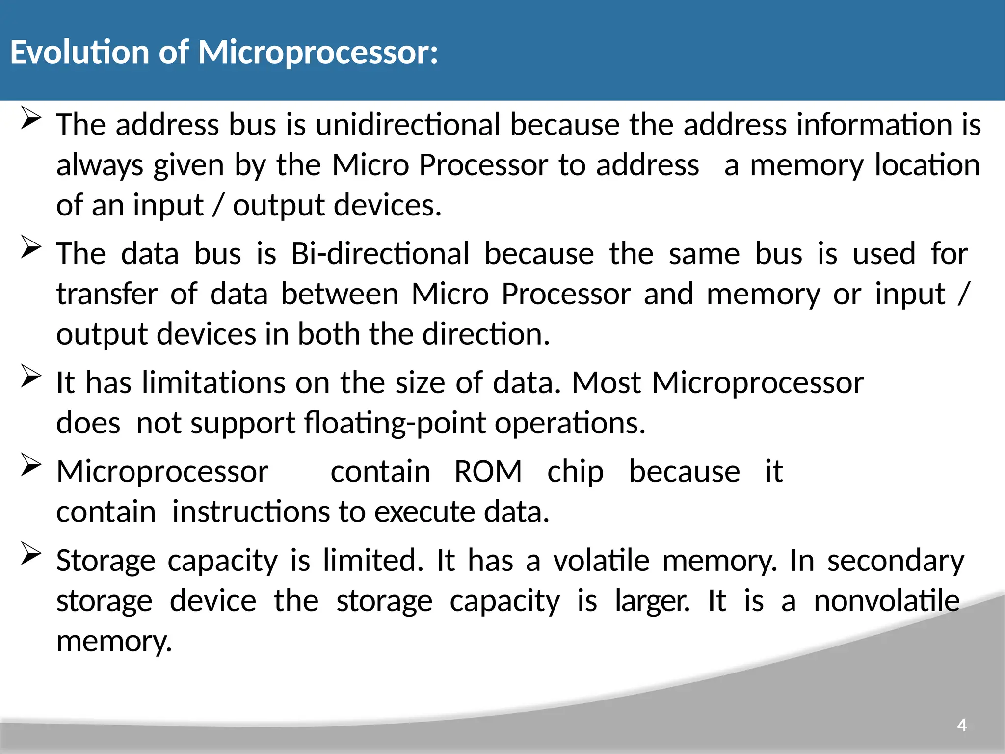
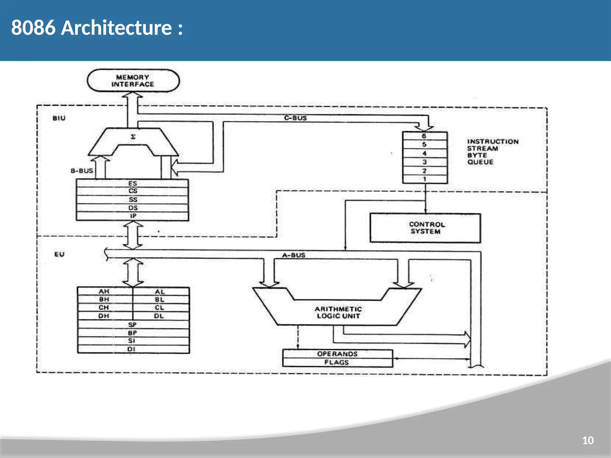
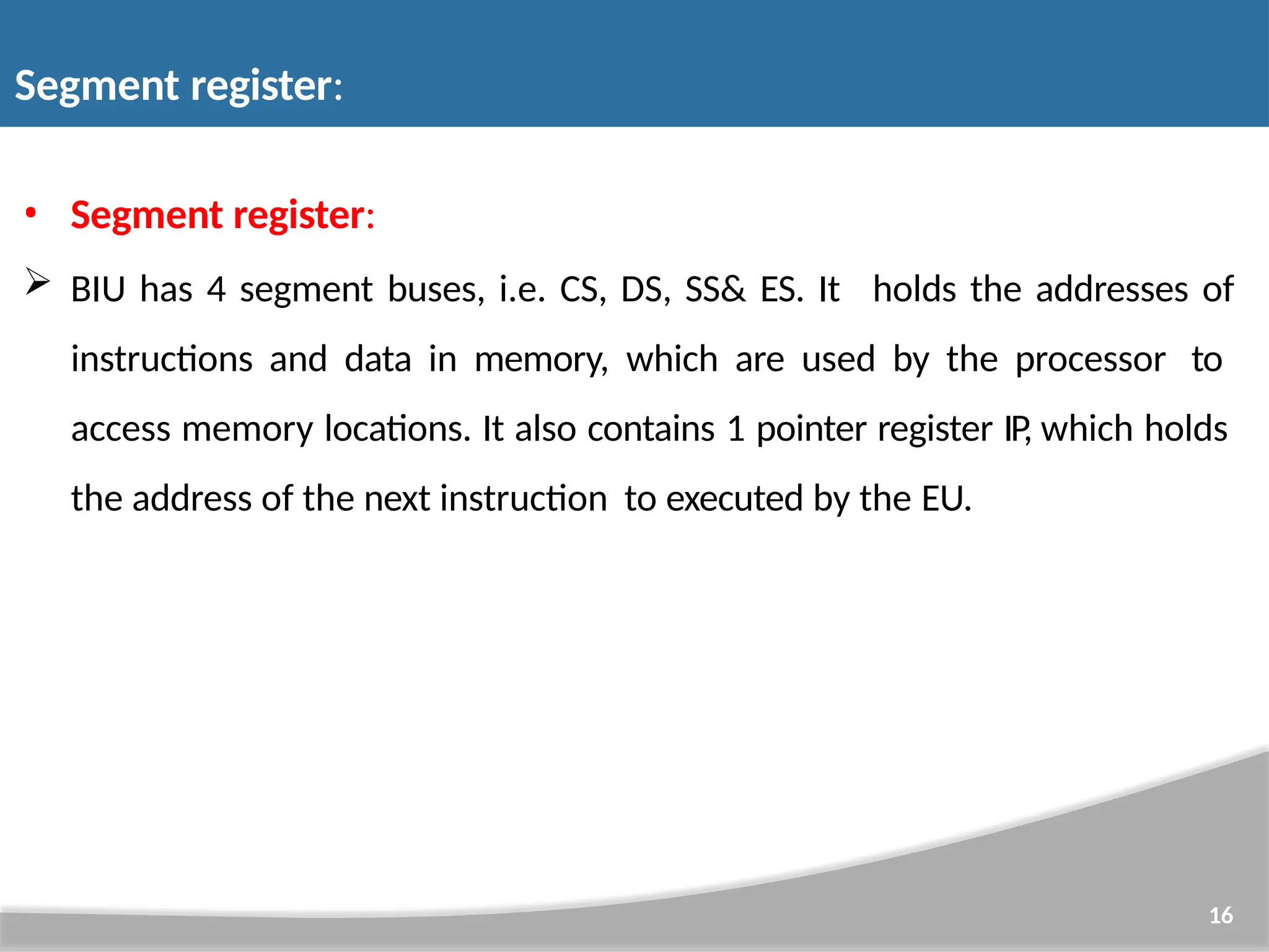
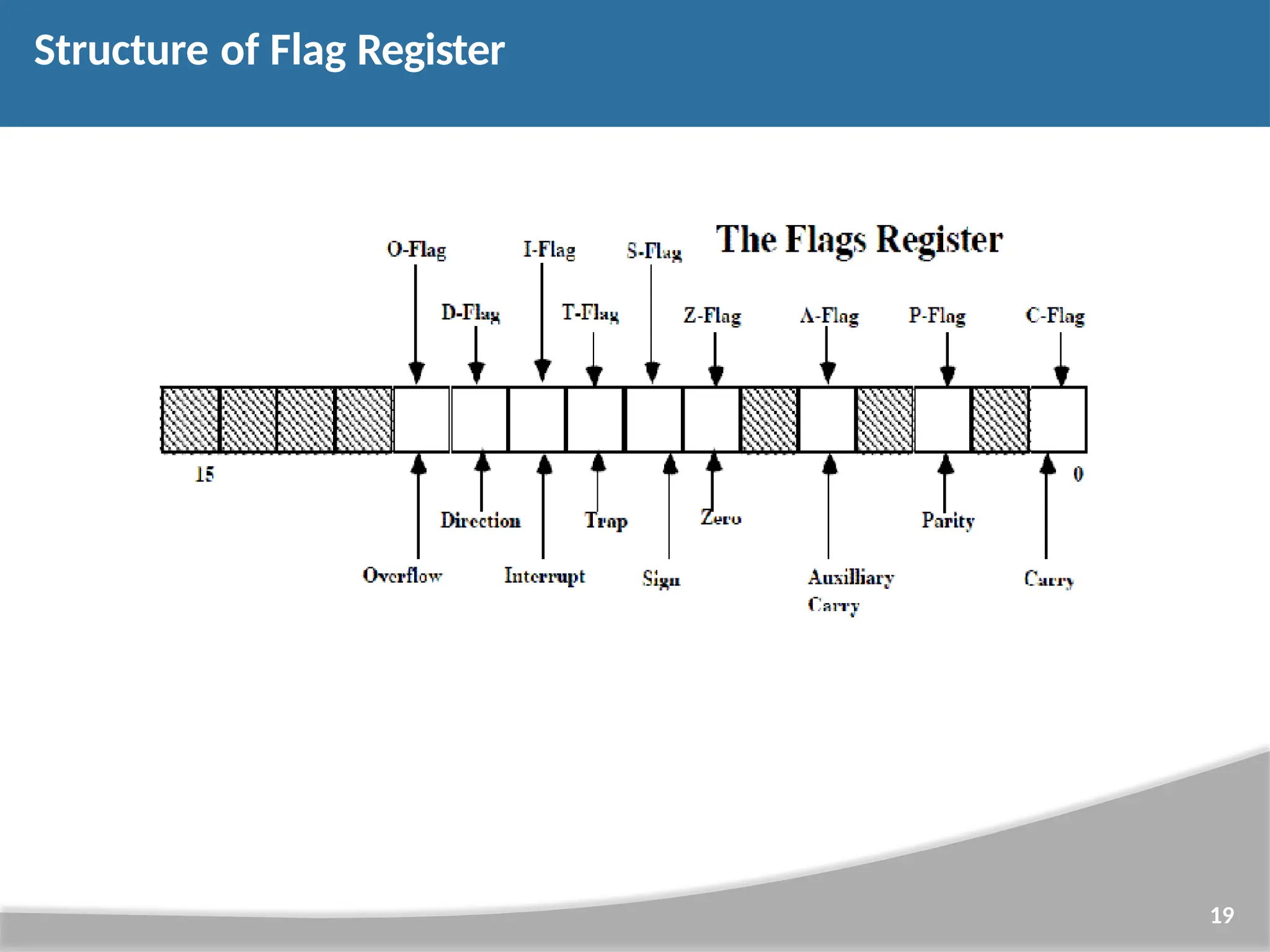
![Direct addressing mode: • In the direct addressing mode, a 16-bit memory address (offset) directly specified in the instruction as a part of it. Example: MOV AX, [5000H]. Register addressing mode: 27 • In the register addressing mode, the data is stored in a register and it is referred using the particular register. All the registers, except IP, used in this mode. may be Example: MOV BX, AX Addressing Modes of 8086](https://image.slidesharecdn.com/mpmcppt1-250630101357-9236328f/75/Microprocessors-Microcontrollers-Architecture-and-Description-27-2048.jpg)
![Register indirect addressing mode: • Sometimes, the address of the memory location which contains data or operands is determined in an indirect way, using the offset registers. The mode of addressing is known as register indirect mode. • In this addressing mode, the offset address of data is in either BX or SI or DI Register. The default segment is either DS or ES. E• xample: MOV AX, [BX]. 28 Addressing Modes of 8086](https://image.slidesharecdn.com/mpmcppt1-250630101357-9236328f/75/Microprocessors-Microcontrollers-Architecture-and-Description-28-2048.jpg)
![Indexed addressing mode: • In this addressing mode, offset of the operand is stored one of the index registers. DS & ES are the default segments for index registers SI & DI respectively. Example: MOV AX, [SI] • Here, data is available at an offset address stored in SI in DS. 29 Addressing Modes of 8086](https://image.slidesharecdn.com/mpmcppt1-250630101357-9236328f/75/Microprocessors-Microcontrollers-Architecture-and-Description-29-2048.jpg)
![Register relative addressing mode: • In this addressing mode, the data is available at an effective address formed by adding an 8-bit or 16-bit displacement with the content of any one of the register BX, BP, SI & DI in the default (either in DS & ES) segment. 30 Example: MOV AX, 50H [BX] Addressing Modes of 8086](https://image.slidesharecdn.com/mpmcppt1-250630101357-9236328f/75/Microprocessors-Microcontrollers-Architecture-and-Description-30-2048.jpg)
![• 31 • Based indexed addressing mode: • The effective address of data is formed in this addressing mode, by adding content of a base register (any one of BX or BP) to the content of an index register (any one of SI or DI). The default segment register may be ES or DS. Example: MOV AX, [BX][SI] Relative based indexed: • The effective address is formed by adding an 8 or 16-bit displacement with the sum of contents of any of the base registers (BX or BP) and any one of the index registers, in a default segment. Example: MOV AX, 50H [BX] [SI] • Addressing Modes of 8086](https://image.slidesharecdn.com/mpmcppt1-250630101357-9236328f/75/Microprocessors-Microcontrollers-Architecture-and-Description-31-2048.jpg)
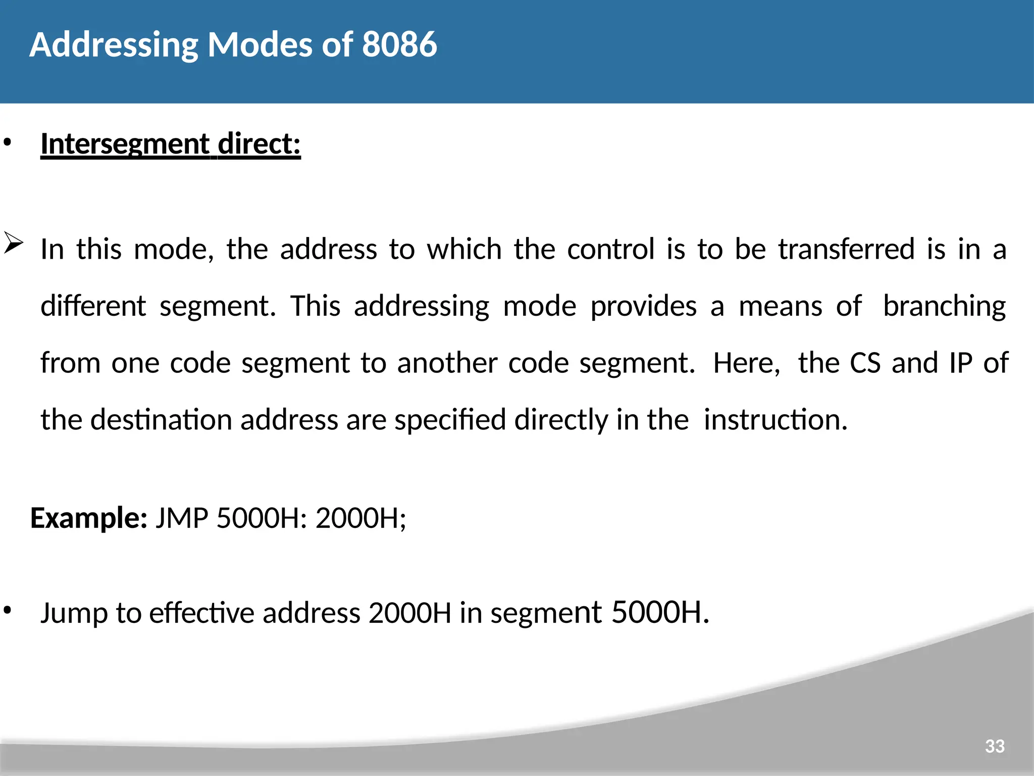
![Intersegment indirect: In this mode, the address to which the control is to be transferred lies in a different segment and it is passed to the instruction indirectly, i.e. contents of a memory block containing four bytes, i.e. IP(LSB), IP(MSB), CS(LSB) and CS(MSB) sequentially. The starting address of the memory block may be referred using any of the addressing modes, except immediate mode. Example: JMP [2000H]. 34 Jump to an address in the other segment specified at effective 2000H in DS. address Addressing Modes of 8086](https://image.slidesharecdn.com/mpmcppt1-250630101357-9236328f/75/Microprocessors-Microcontrollers-Architecture-and-Description-34-2048.jpg)
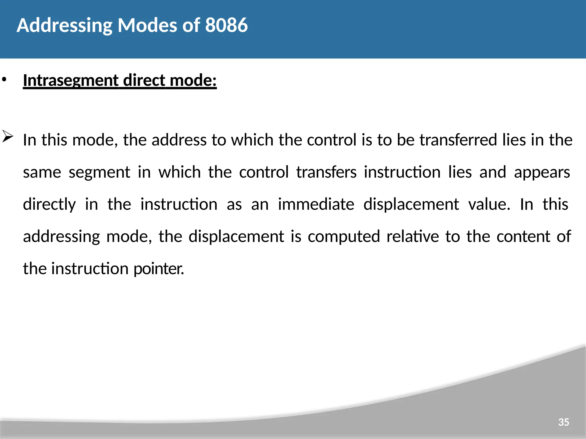
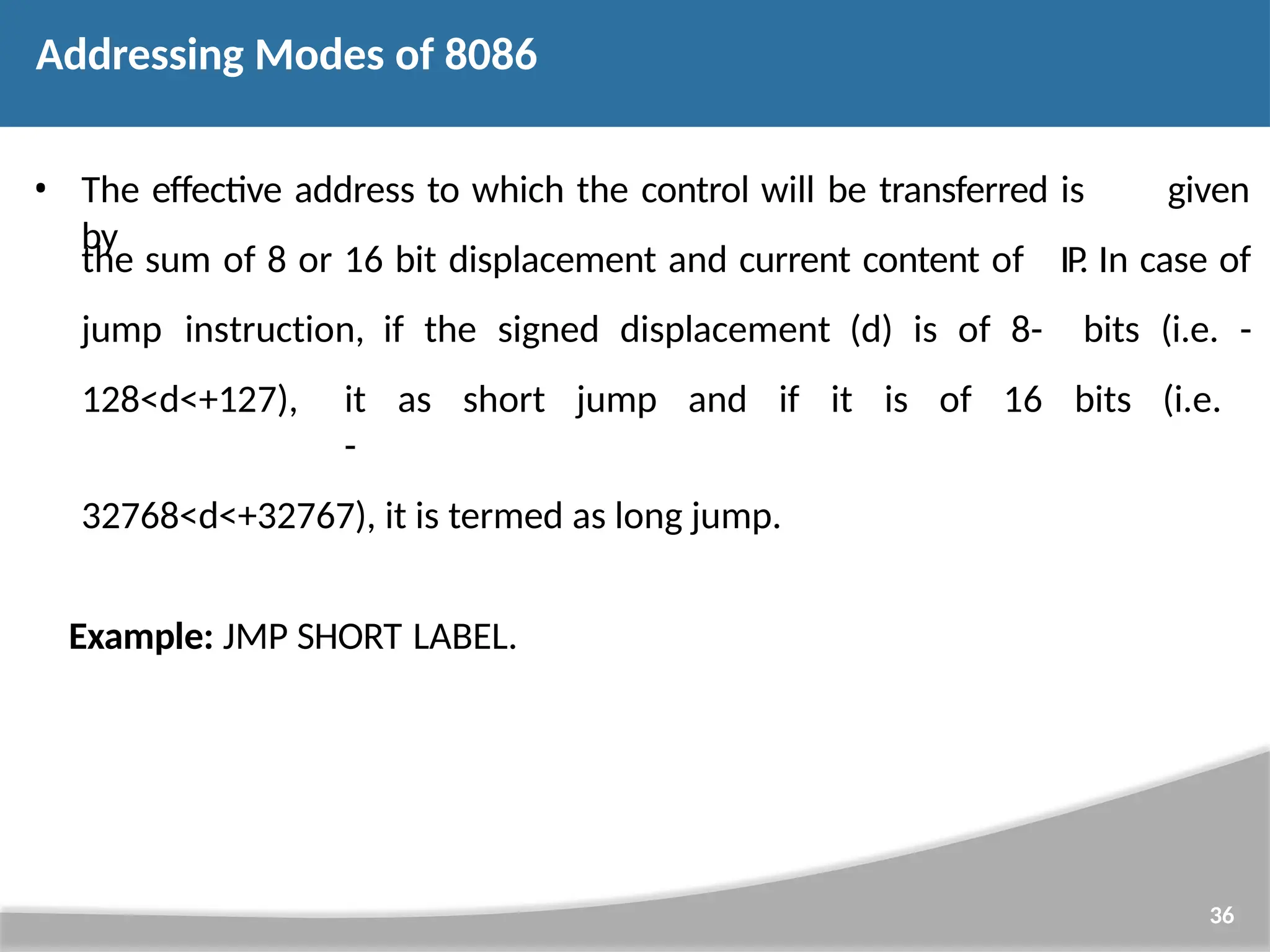
![• Intrasegment indirect mode: • In this mode, the displacement to which the control is to be transferred is in the same segment in which the control transfer instruction lies, but it is passed to the instruction directly. Here, the branch address is found as the content of a register or a memory location. • This addressing mode may be used in unconditional branch instructions. • Example: JMP [BX]; Jump to effective address stored in BX. 37 Addressing Modes of 8086](https://image.slidesharecdn.com/mpmcppt1-250630101357-9236328f/75/Microprocessors-Microcontrollers-Architecture-and-Description-37-2048.jpg)
![General Form: • MOV destination, source • Here the source and destination needs to be of the same size, that is both 8 bit or both 16 bit. • MOV instruction does not affect any flags. Example:- 40 • • MOV BX, 00F2H; load the immediate number 00F2H in BX register • MOV CL, [2000H] ;Copy the 8 bit content of the memory location, at a displacement of2000H from data segment base to the CL register Data Transfer instructions](https://image.slidesharecdn.com/mpmcppt1-250630101357-9236328f/75/Microprocessors-Microcontrollers-Architecture-and-Description-40-2048.jpg)
![•MOV [589H], BX; Copy the 16 bit content of BX register on to the memory location, which at a displacement of 589H from the data segment base. • MOV DS, CX; Move the content of CX to DS PUSH instruction • The PUSH instruction decrements the stack pointer by two and copies the word from source to the location where stack pointer now points. Here the source must of word size data. Source can be a general purpose register, segment register or a memory location. 41 Data Transfer instructions](https://image.slidesharecdn.com/mpmcppt1-250630101357-9236328f/75/Microprocessors-Microcontrollers-Architecture-and-Description-41-2048.jpg)
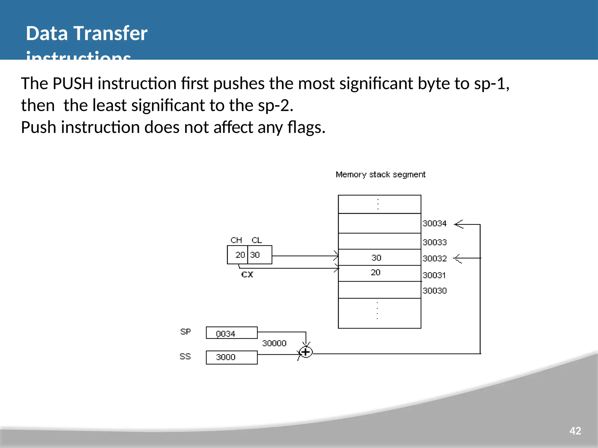
![XCHG instruction • The XCHG instruction exchanges contents of the destination and source. Here destination and source can be register and register or register and memory location, but XCHG cannot interchange the value of 2 memory locations. General Format • XCHG Destination, Source Example: • XCHG BX, CX; exchange word in CX with the word in BX • XCHG AL, CL; exchange byte in CL with the byte in AL • XCHG AX, SUM[BX];here physical address, which is DS+SUM+[BX]. The content at physical address and the content of AX are interchanged. 45 Data Transfer instructions](https://image.slidesharecdn.com/mpmcppt1-250630101357-9236328f/75/Microprocessors-Microcontrollers-Architecture-and-Description-45-2048.jpg)
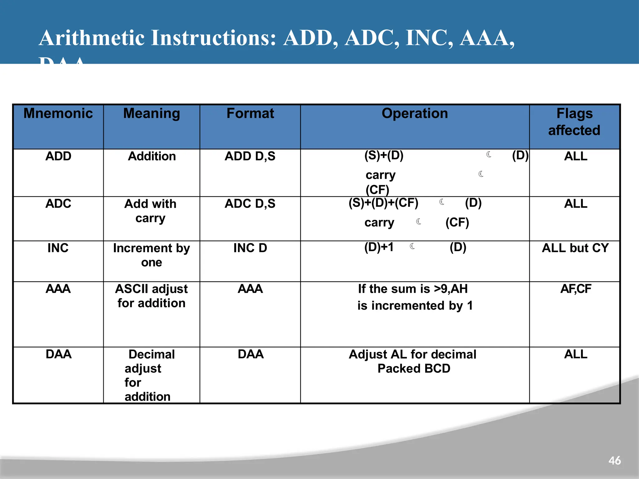
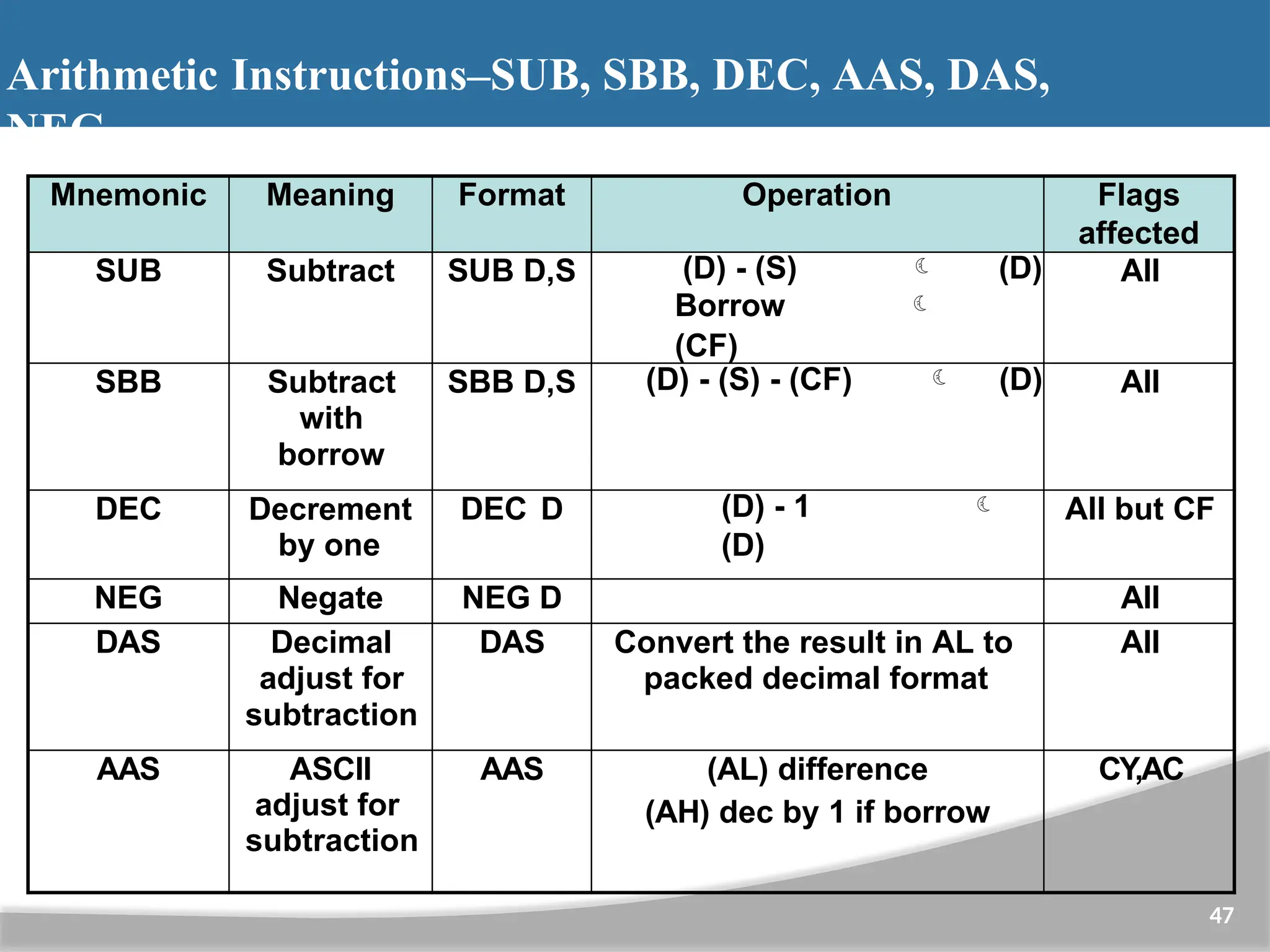
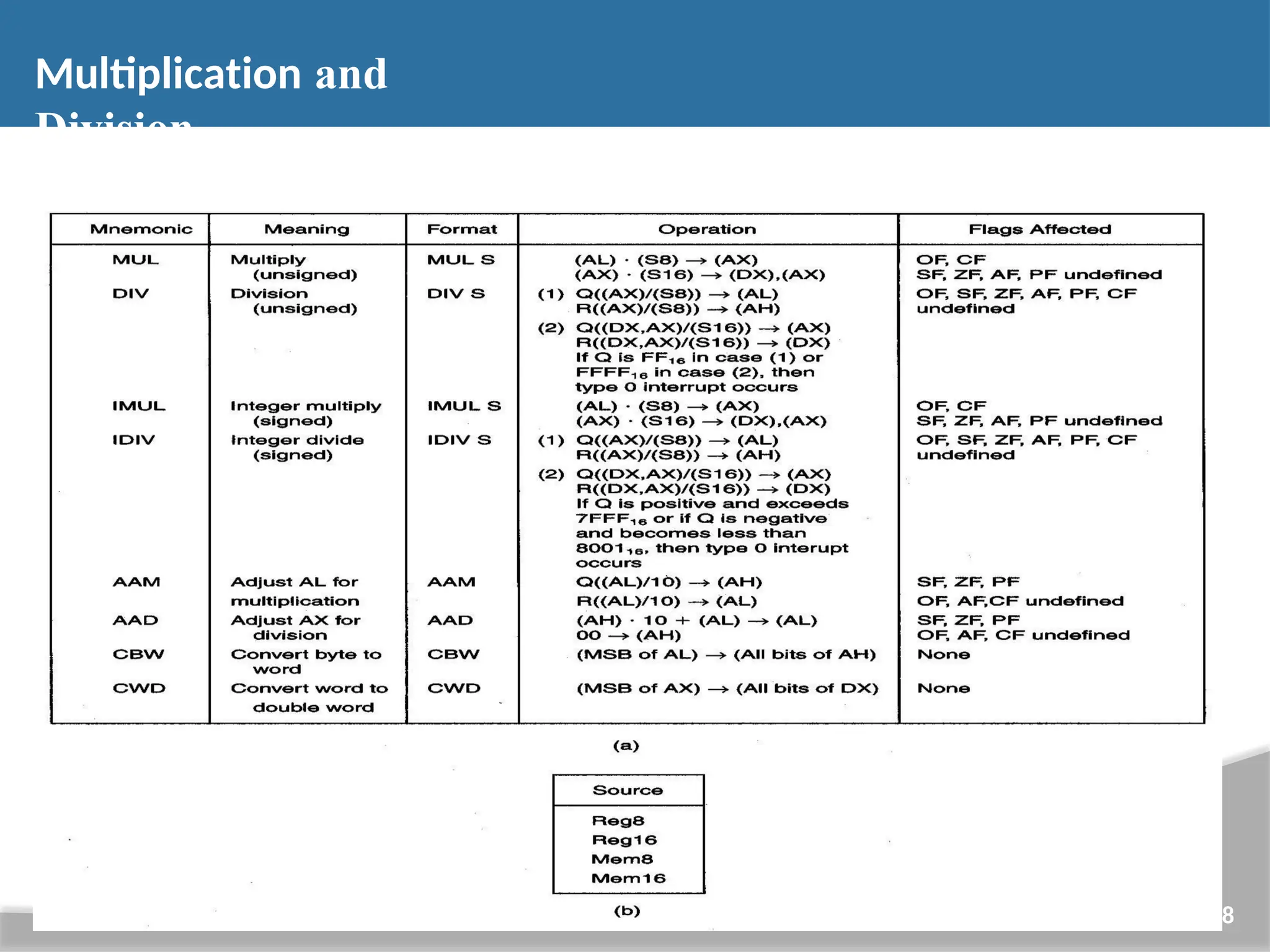
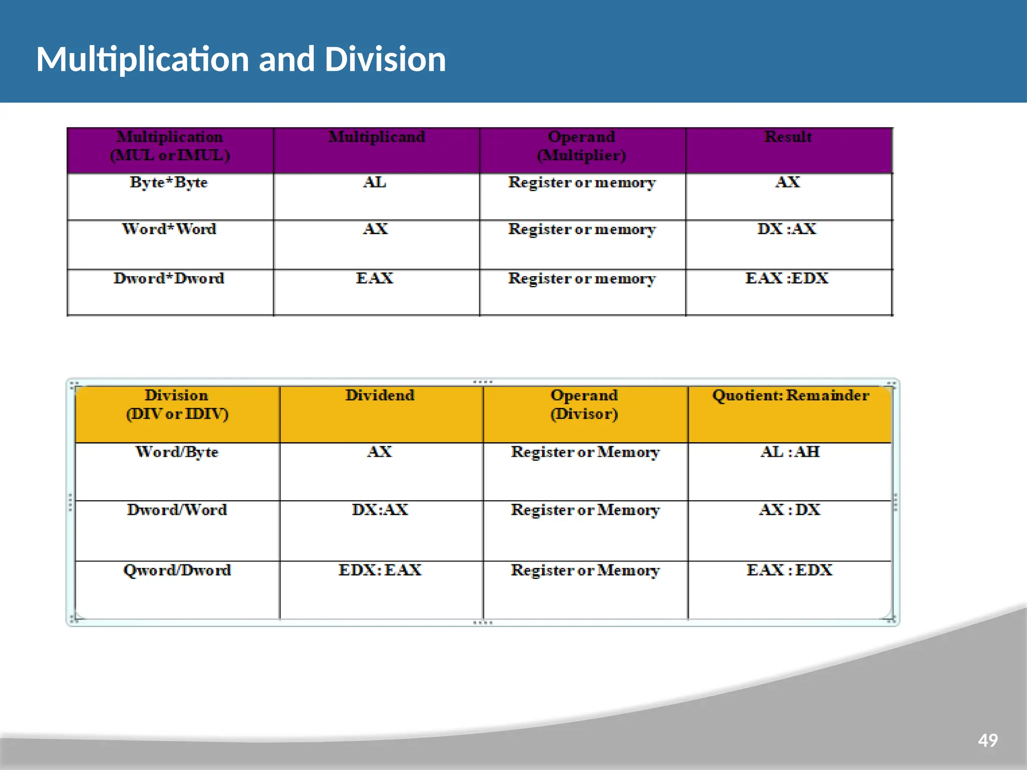
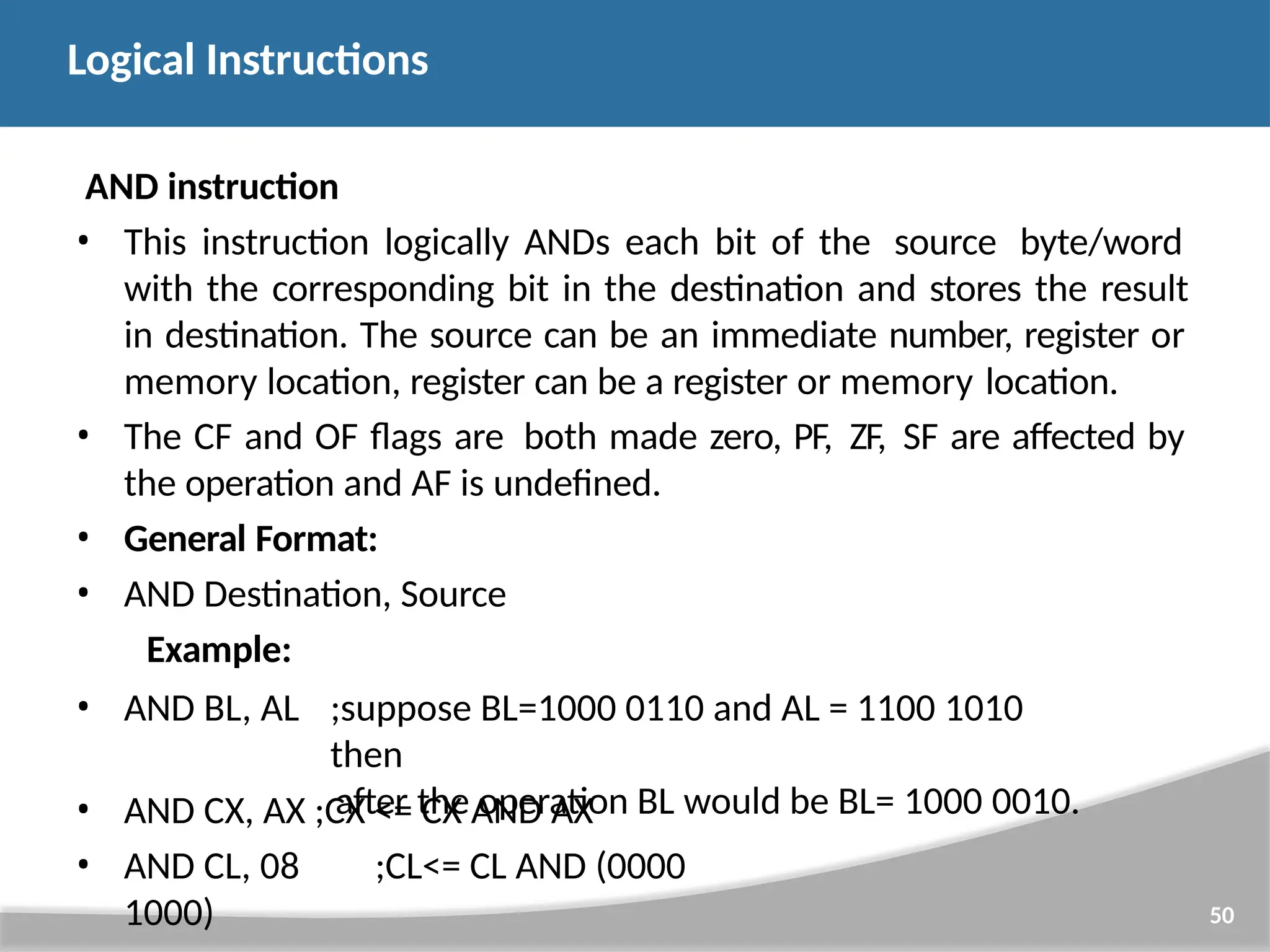
![Example: • OR BL, AL; suppose BL=1000 0110 and AL = 1100 1010 then after the operation BL would be BL= 1100 1110. • OR CX, AX;CX <= CX AND AX • OR CL, 08;CL<= CL AND (0000 1000) NOT instruction • The NOT instruction complements (inverts) the contents of an operand register or a memory location, bit by bit. The examples are as follows: Example: • NOT AX (BEFORE AX= (1011)2= (B) 16 AFTER EXECUTION AX= (0100)2= (4)16). • NOT [5000H] 52 Logical Instructions](https://image.slidesharecdn.com/mpmcppt1-250630101357-9236328f/75/Microprocessors-Microcontrollers-Architecture-and-Description-52-2048.jpg)
![XOR instruction • The XOR operation is again carried out in a similar way to the AND and OR operation. The constraints on the operands are also similar. The XOR operation gives a high output, when the 2 input bits are dissimilar. Otherwise, the output is zero. The example instructions are as follows: Example: • XOR AX,0098H • XOR AX,BX • XOR AX,[5000H] 53 Logical Instructions](https://image.slidesharecdn.com/mpmcppt1-250630101357-9236328f/75/Microprocessors-Microcontrollers-Architecture-and-Description-53-2048.jpg)
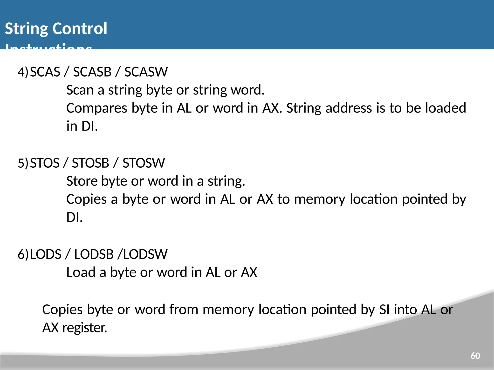
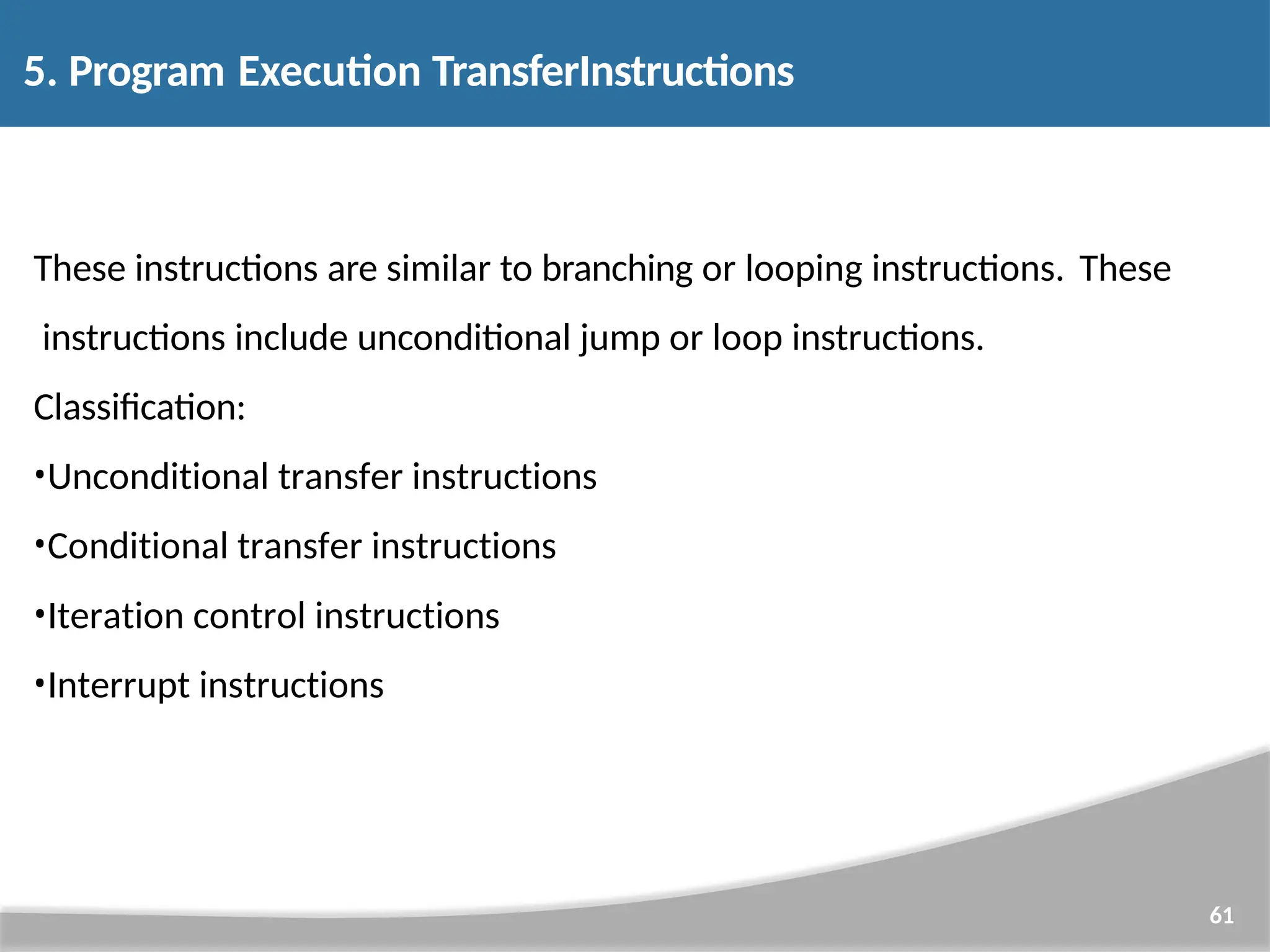
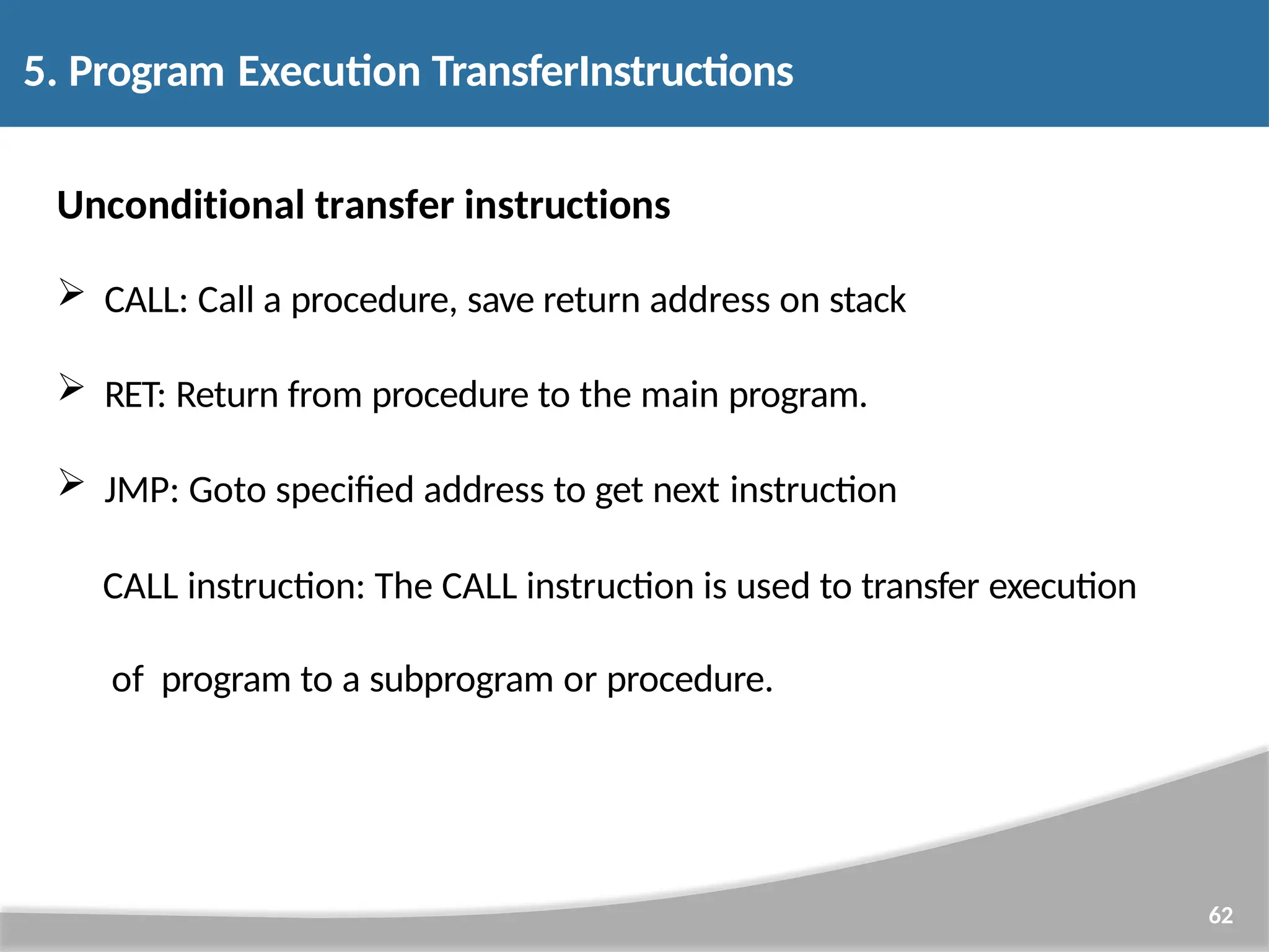
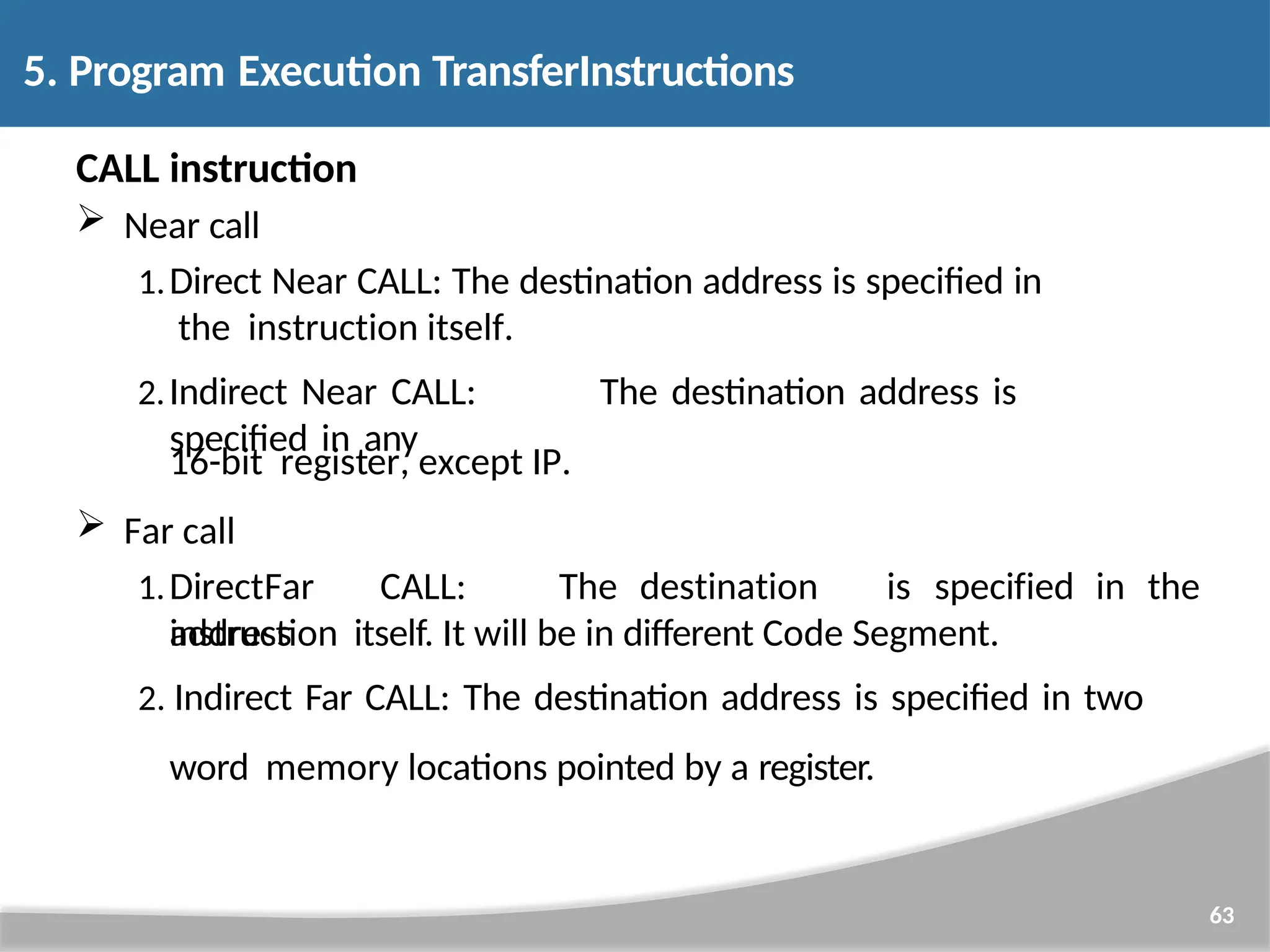
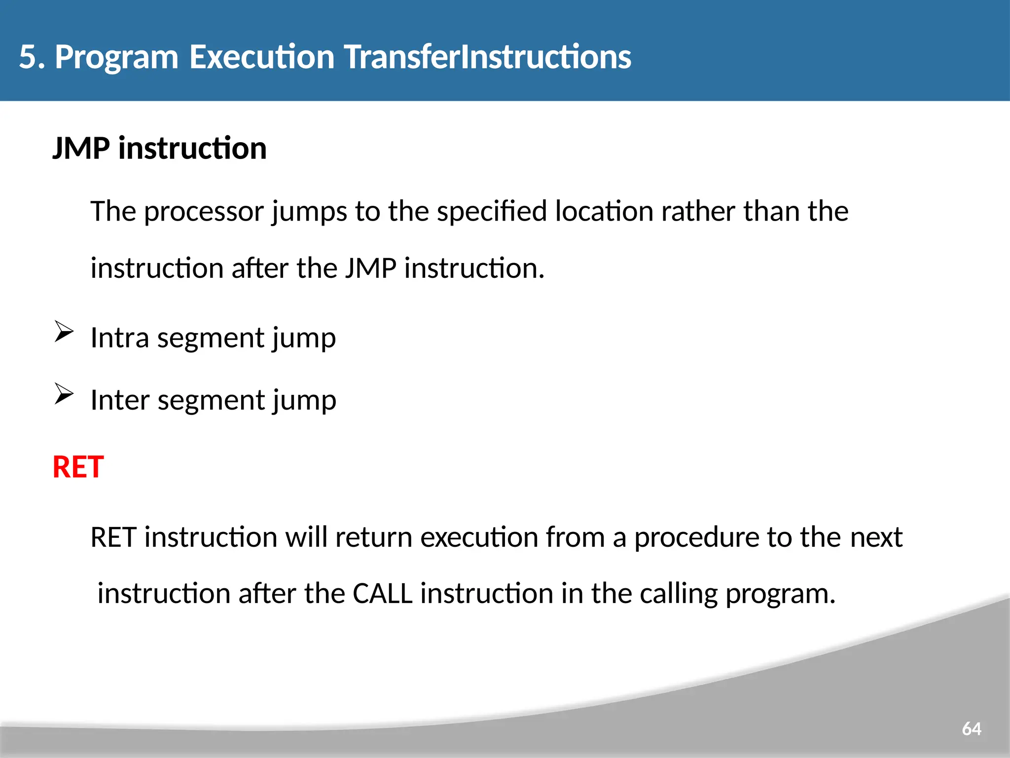
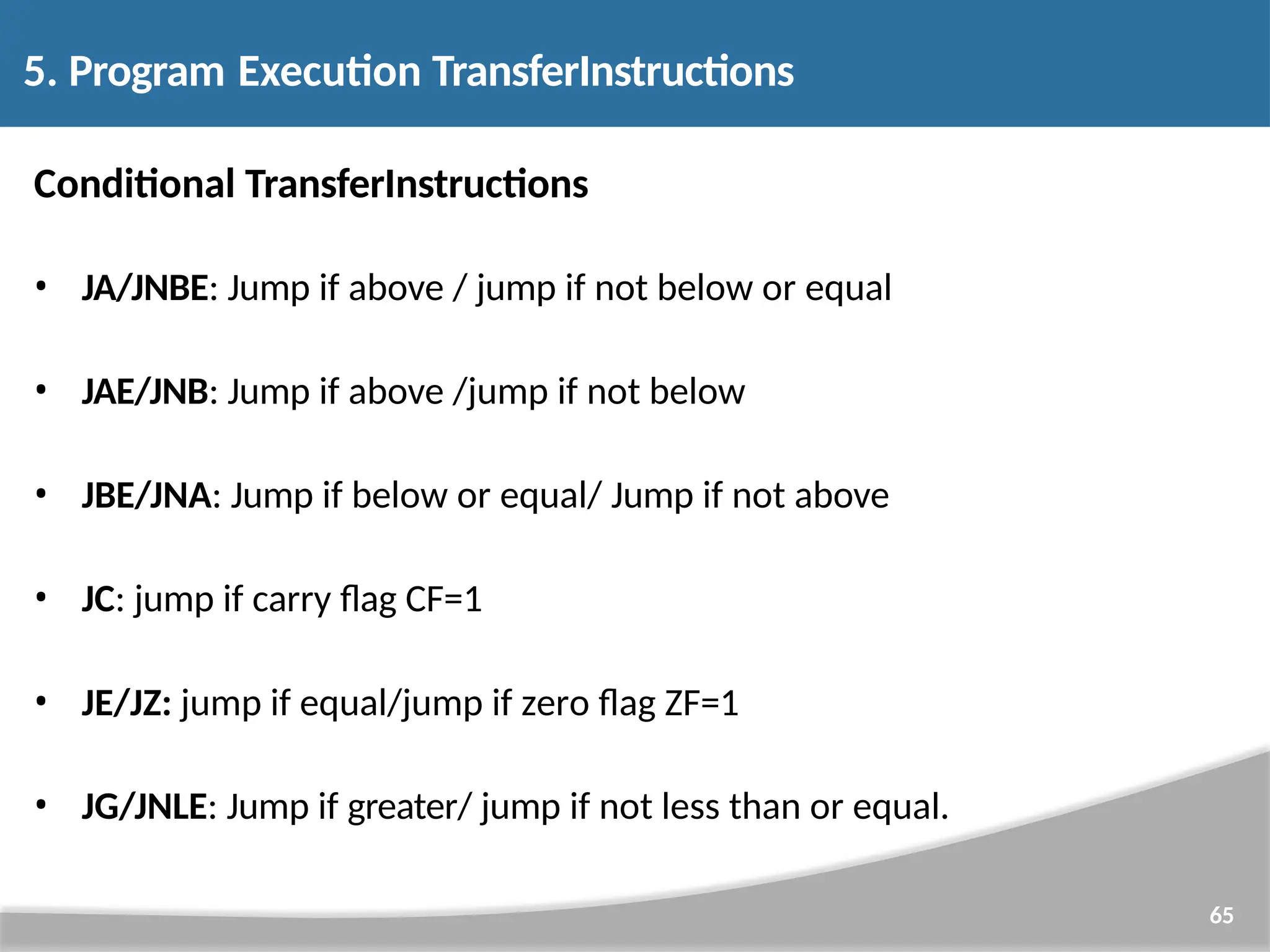
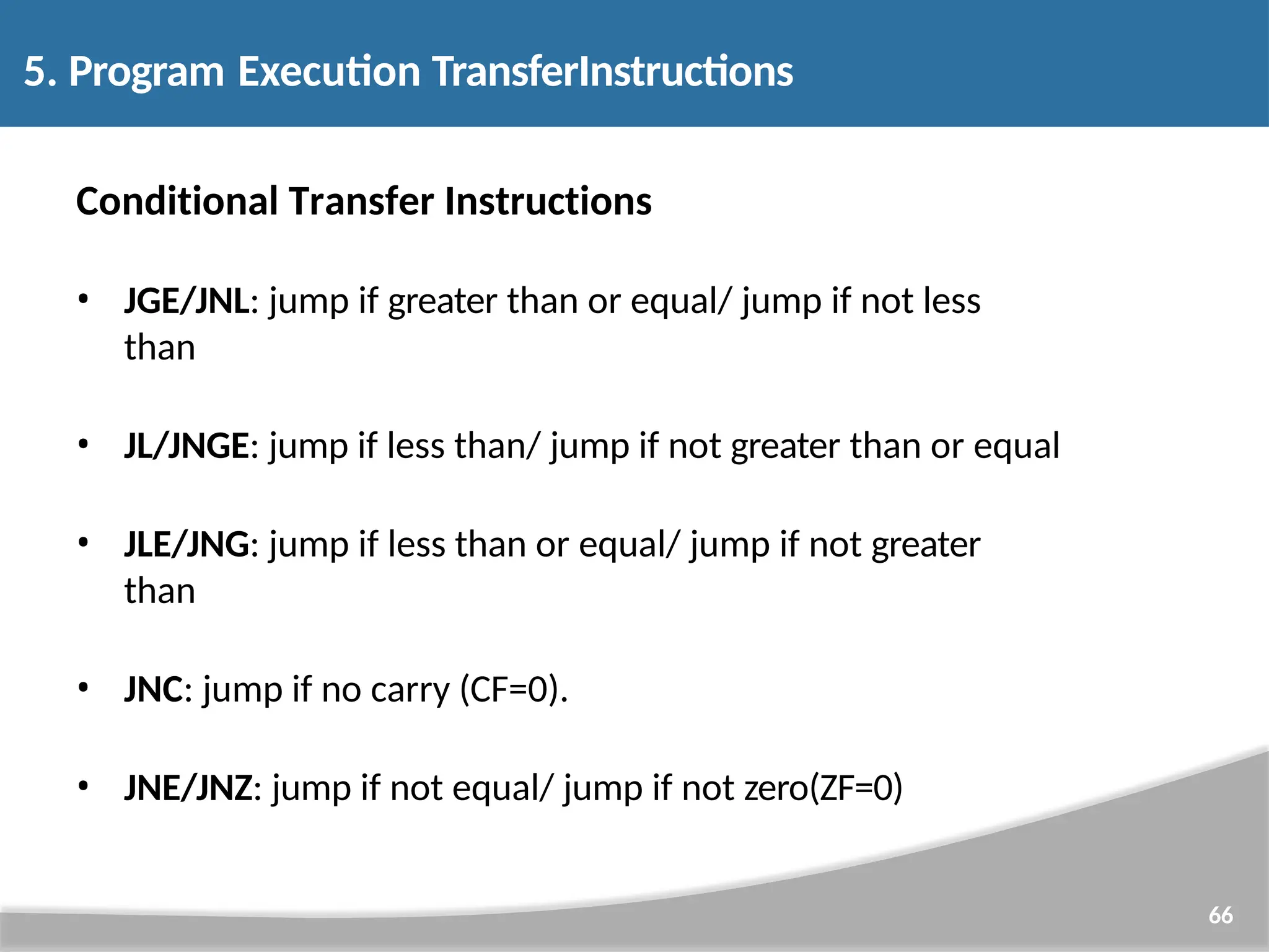
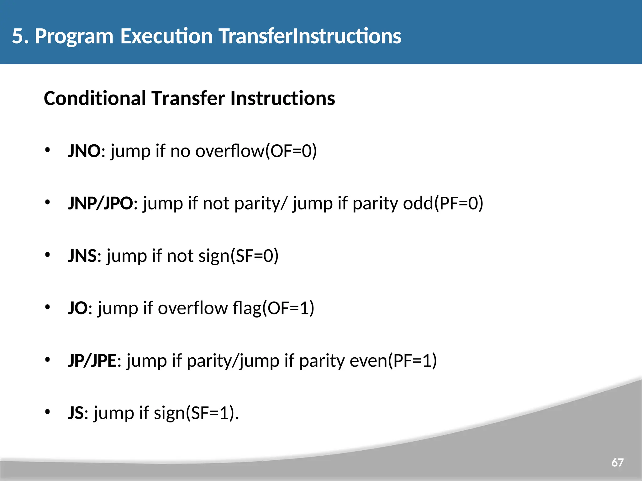
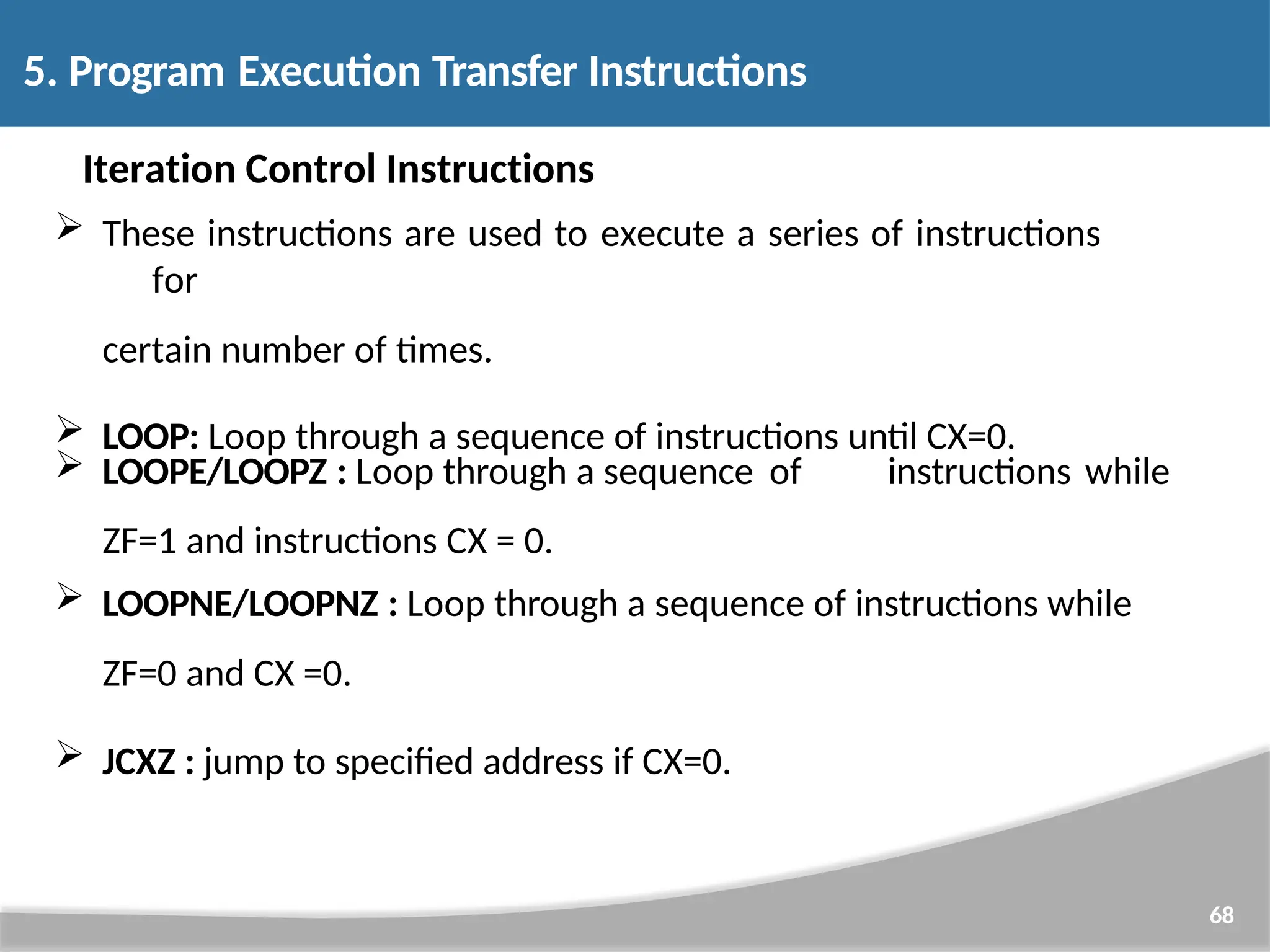
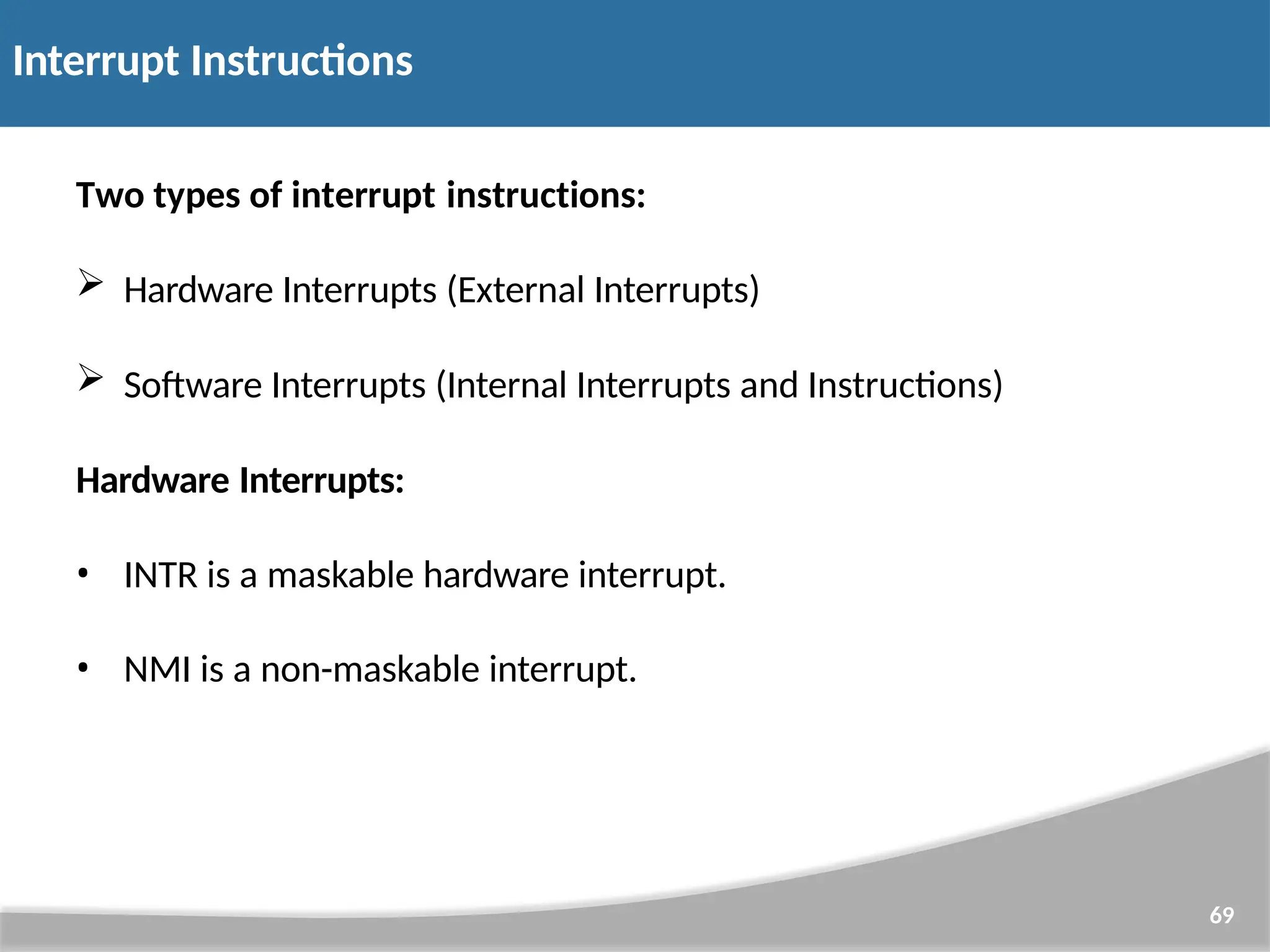
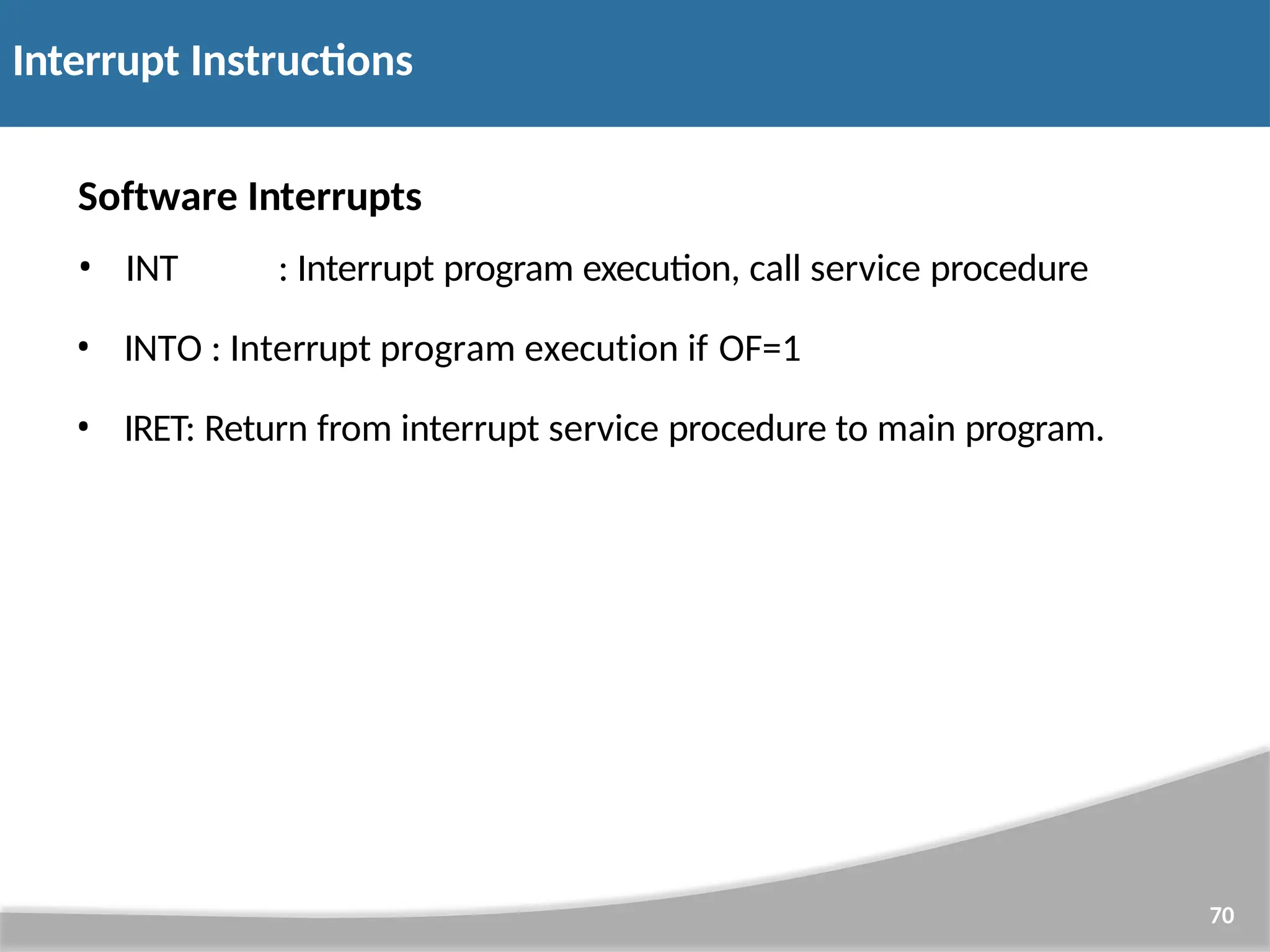
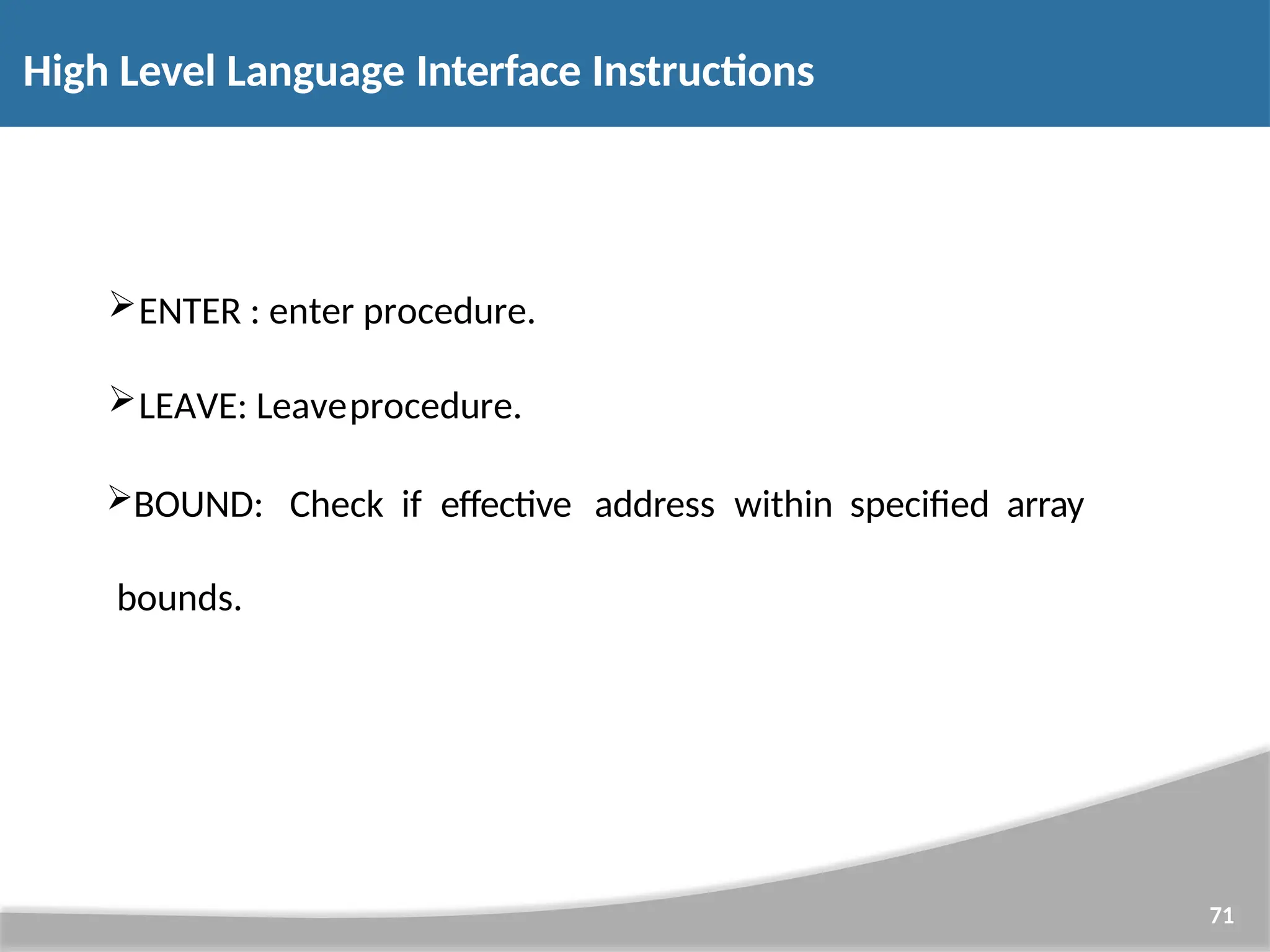
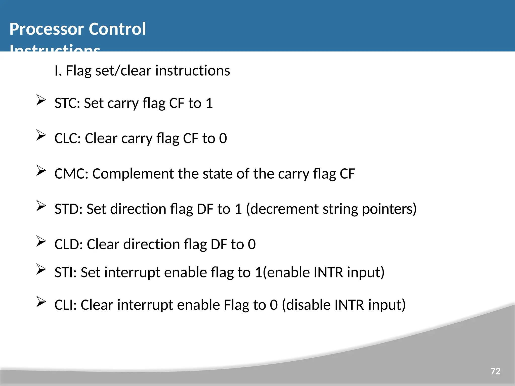
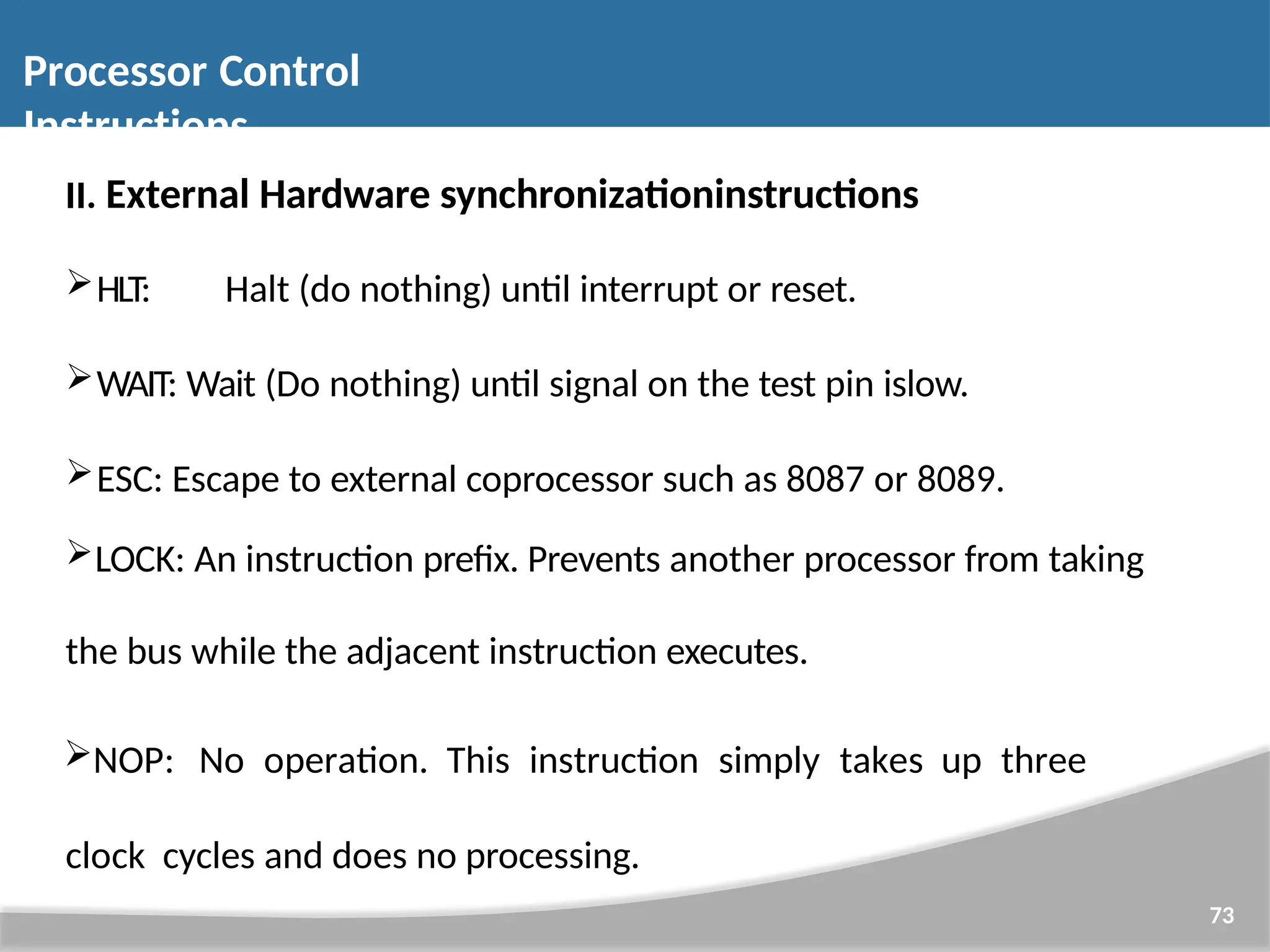
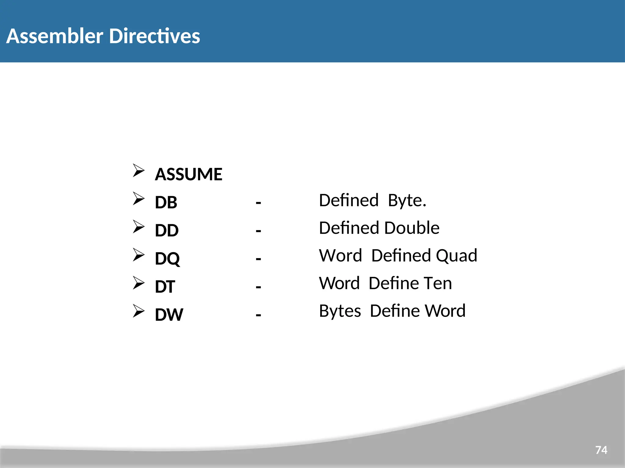
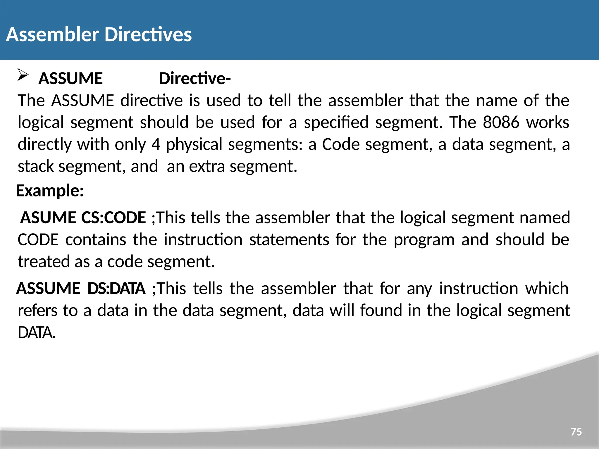
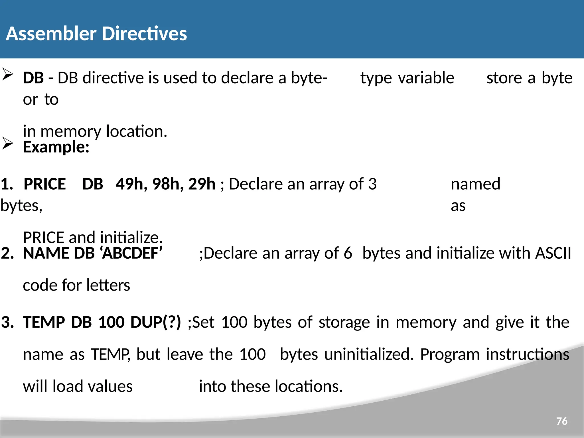
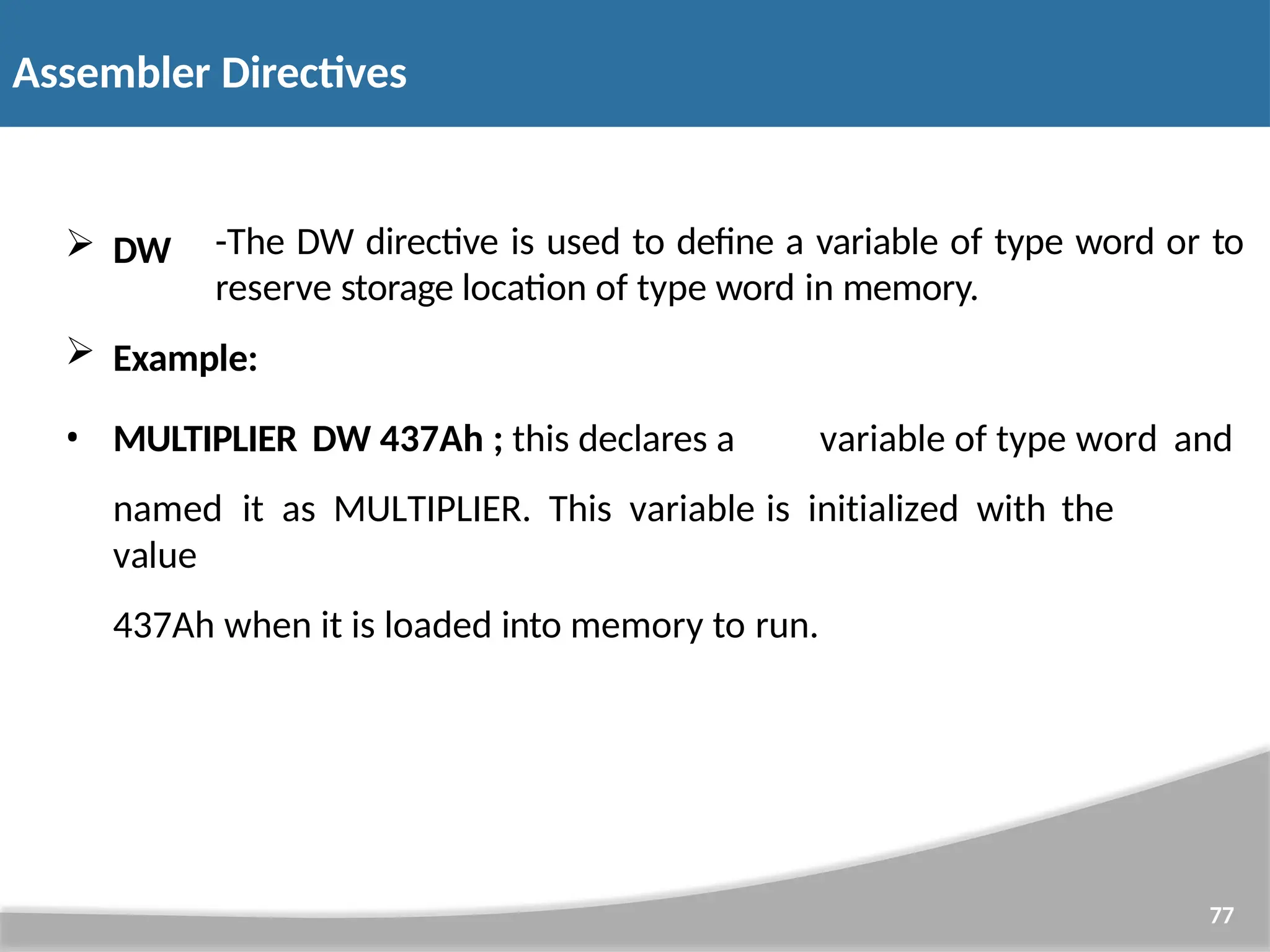
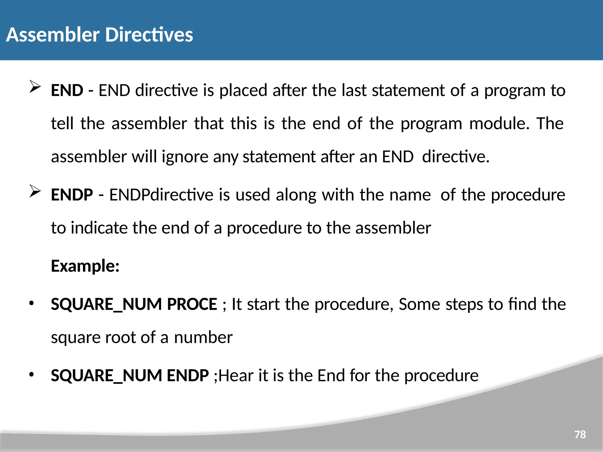
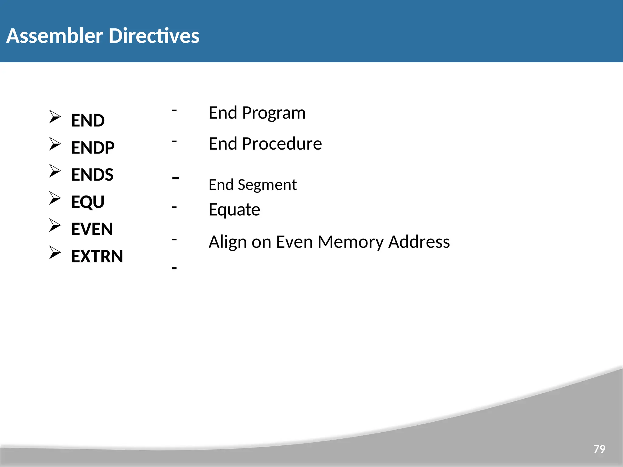
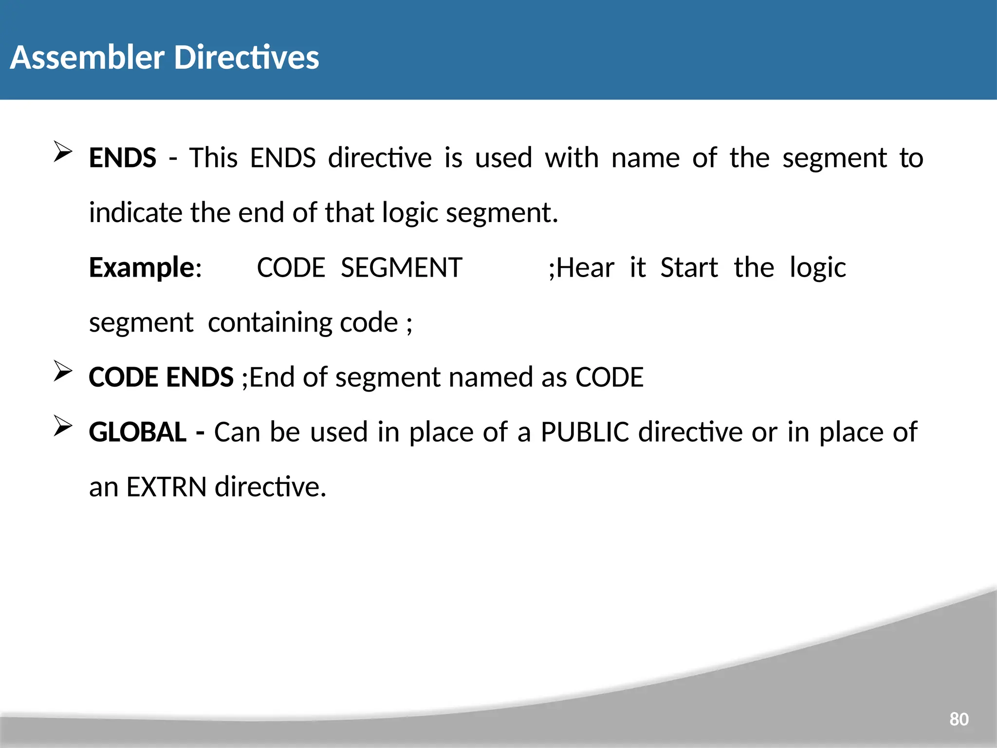
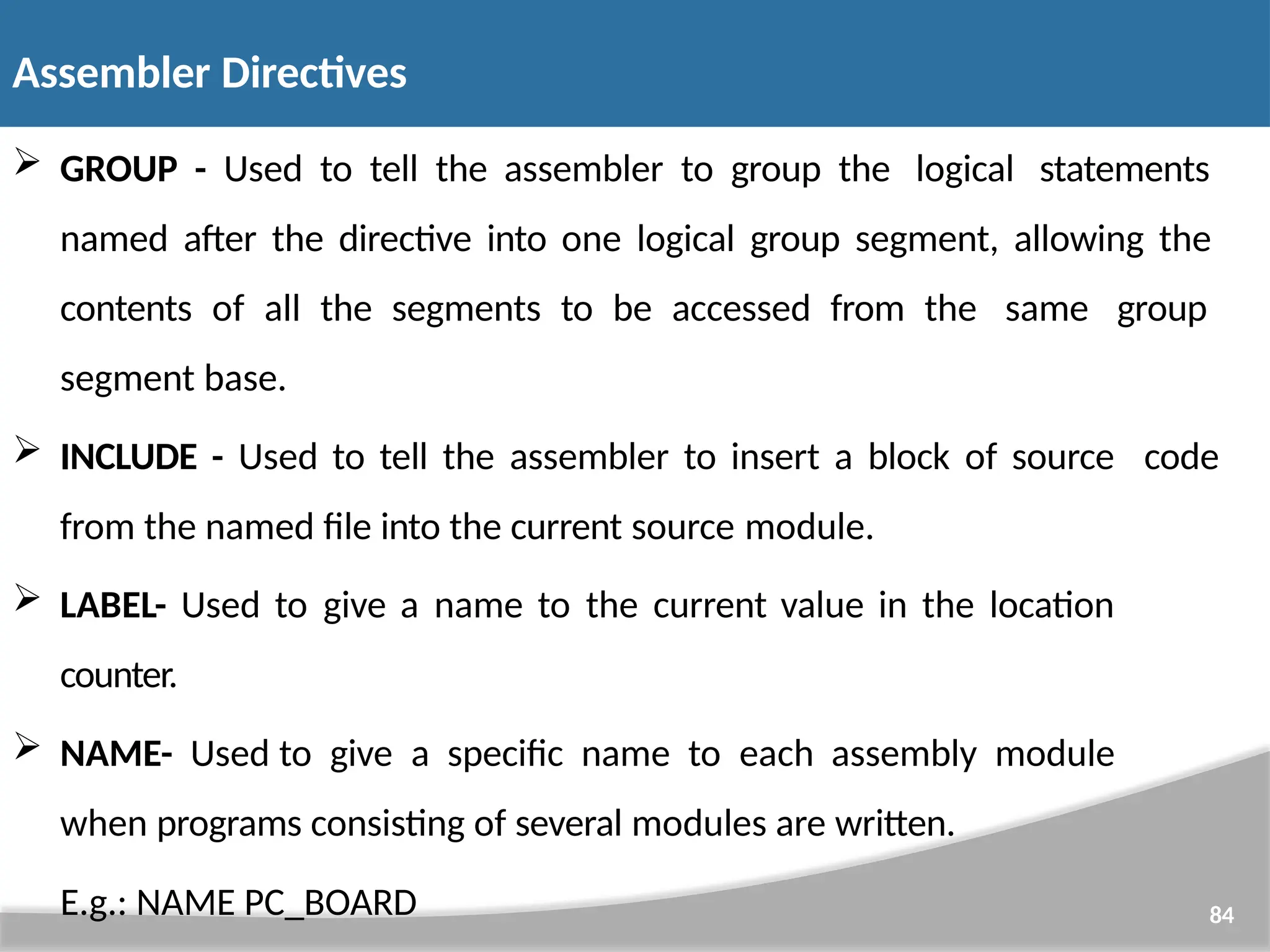
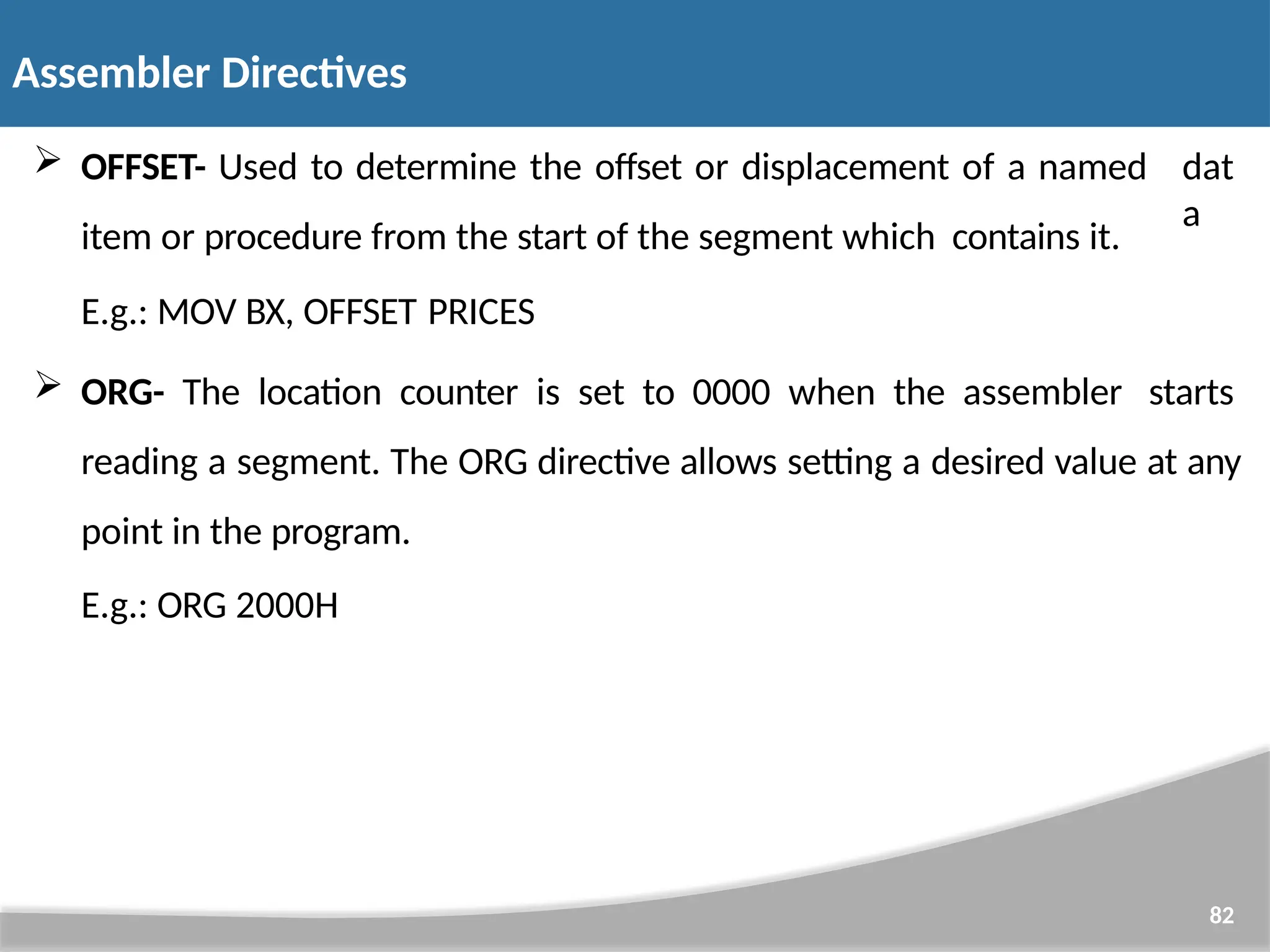
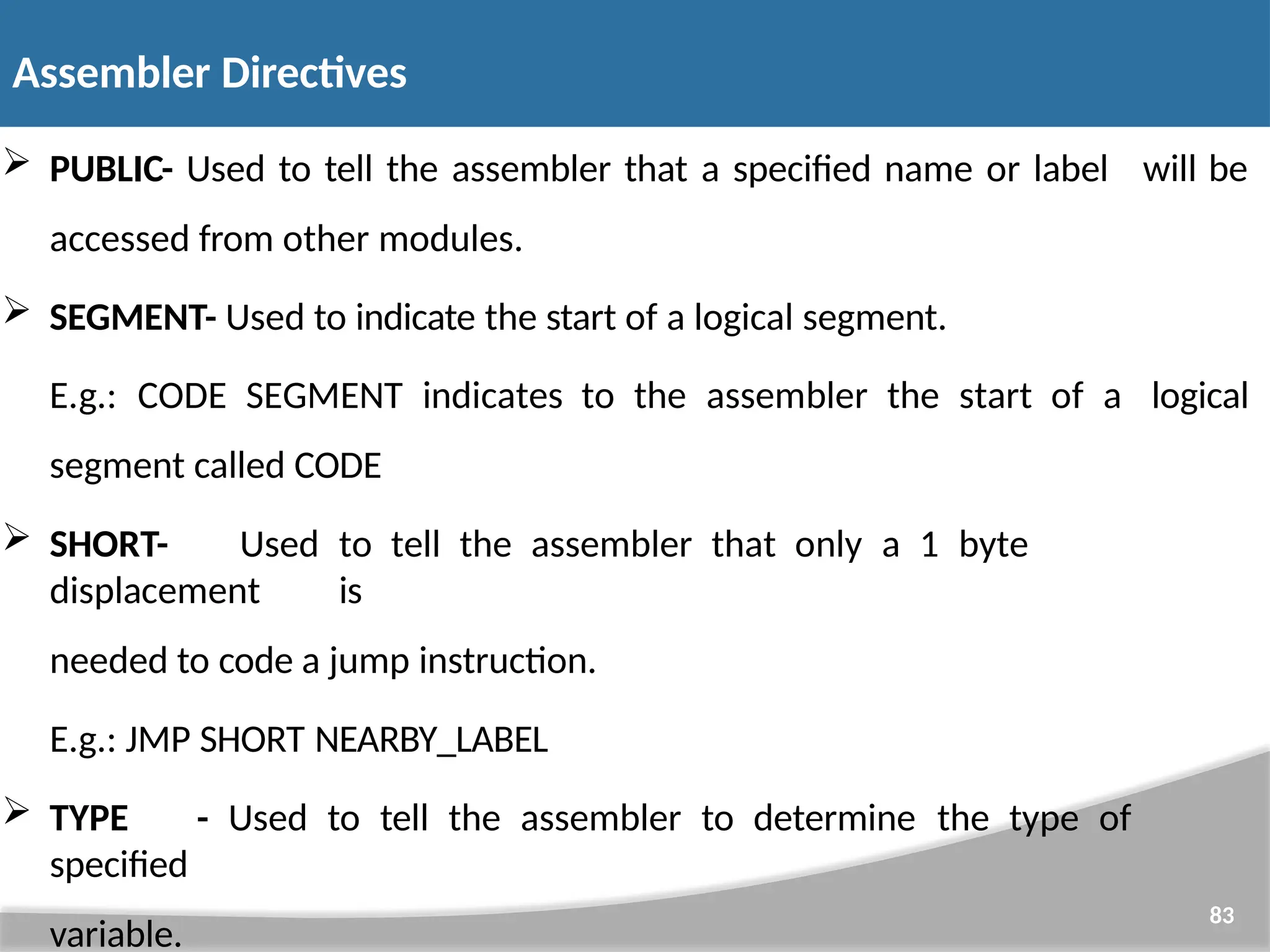
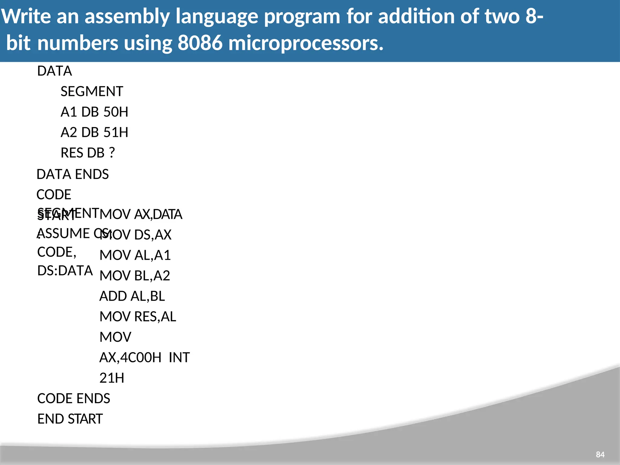
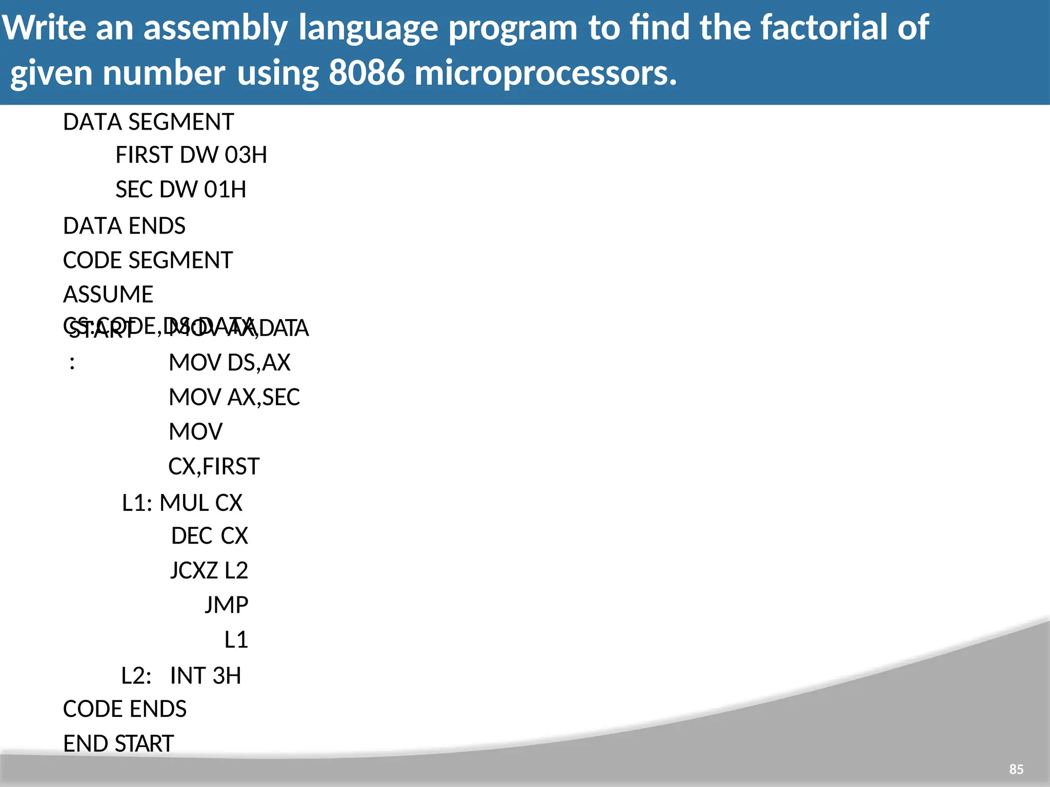
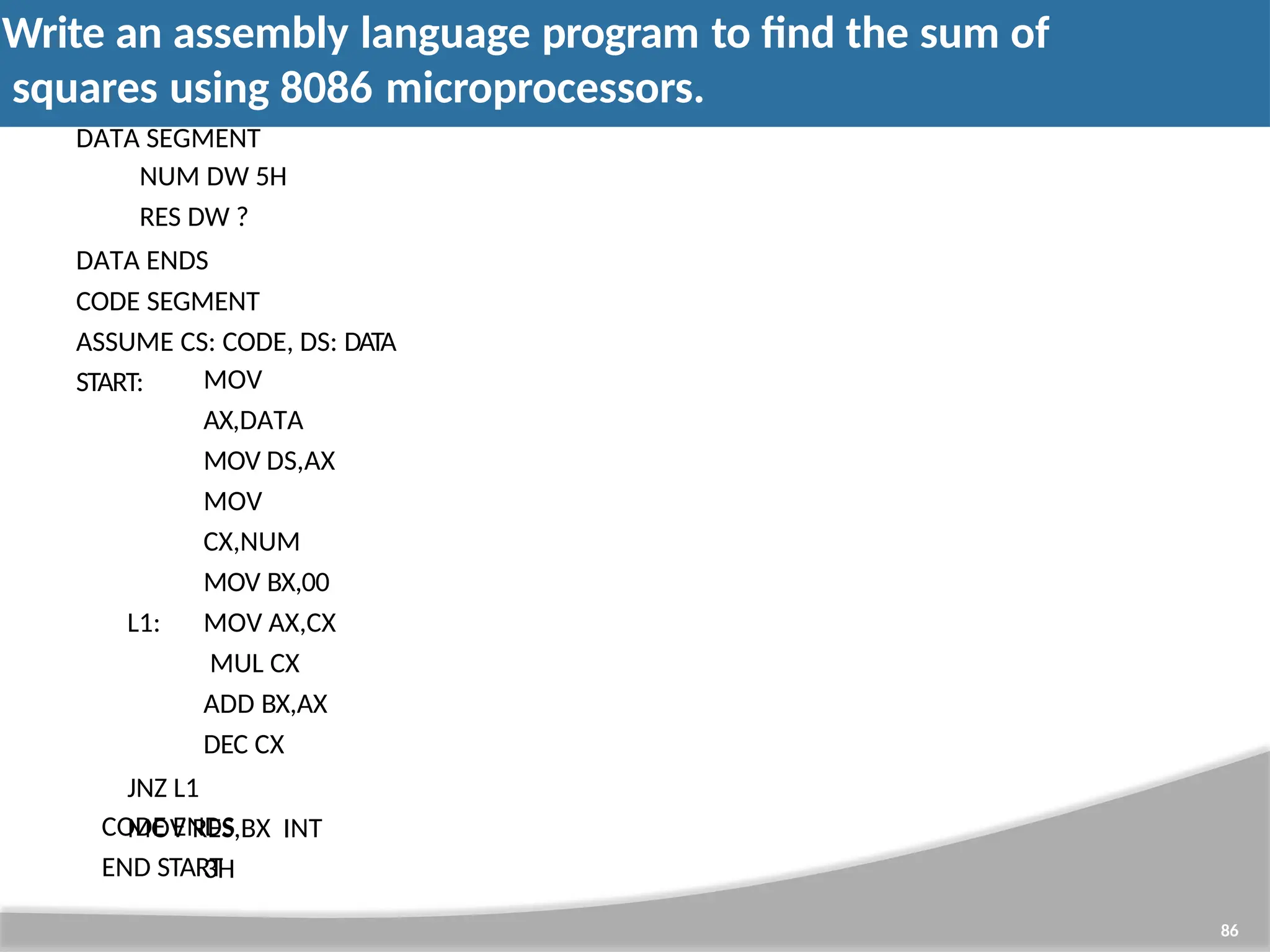
![Procedures: • While writing programs, it may be the case that a particular sequence of instructions is used several times. To avoid writing the sequence of instructions again and again in the program, the same sequence can be written as a separate subprogram called a procedure. Defining Procedures: 87 • Assembler provides PROC and ENDP directives in order to define procedures. The directive PROC indicates beginning of a procedure. Its general form is: Procedure_name PROC [NEAR|FAR] Procedures and Macros](https://image.slidesharecdn.com/mpmcppt1-250630101357-9236328f/75/Microprocessors-Microcontrollers-Architecture-and-Description-87-2048.jpg)
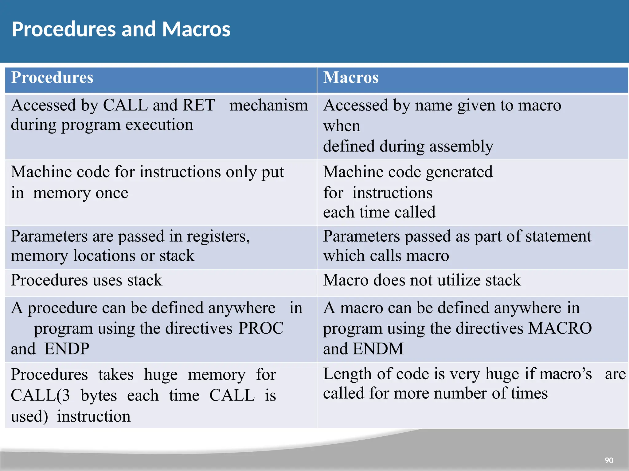
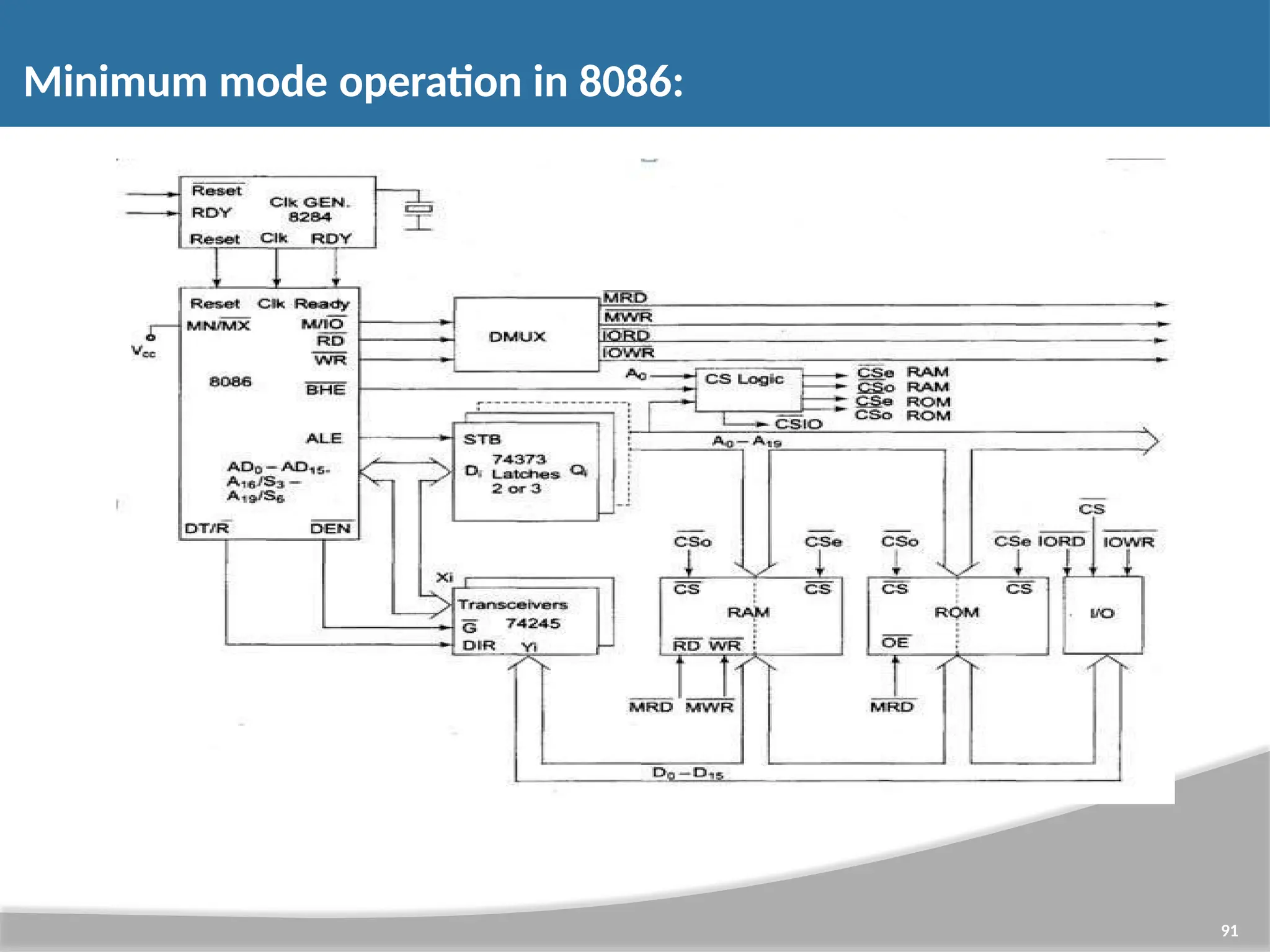
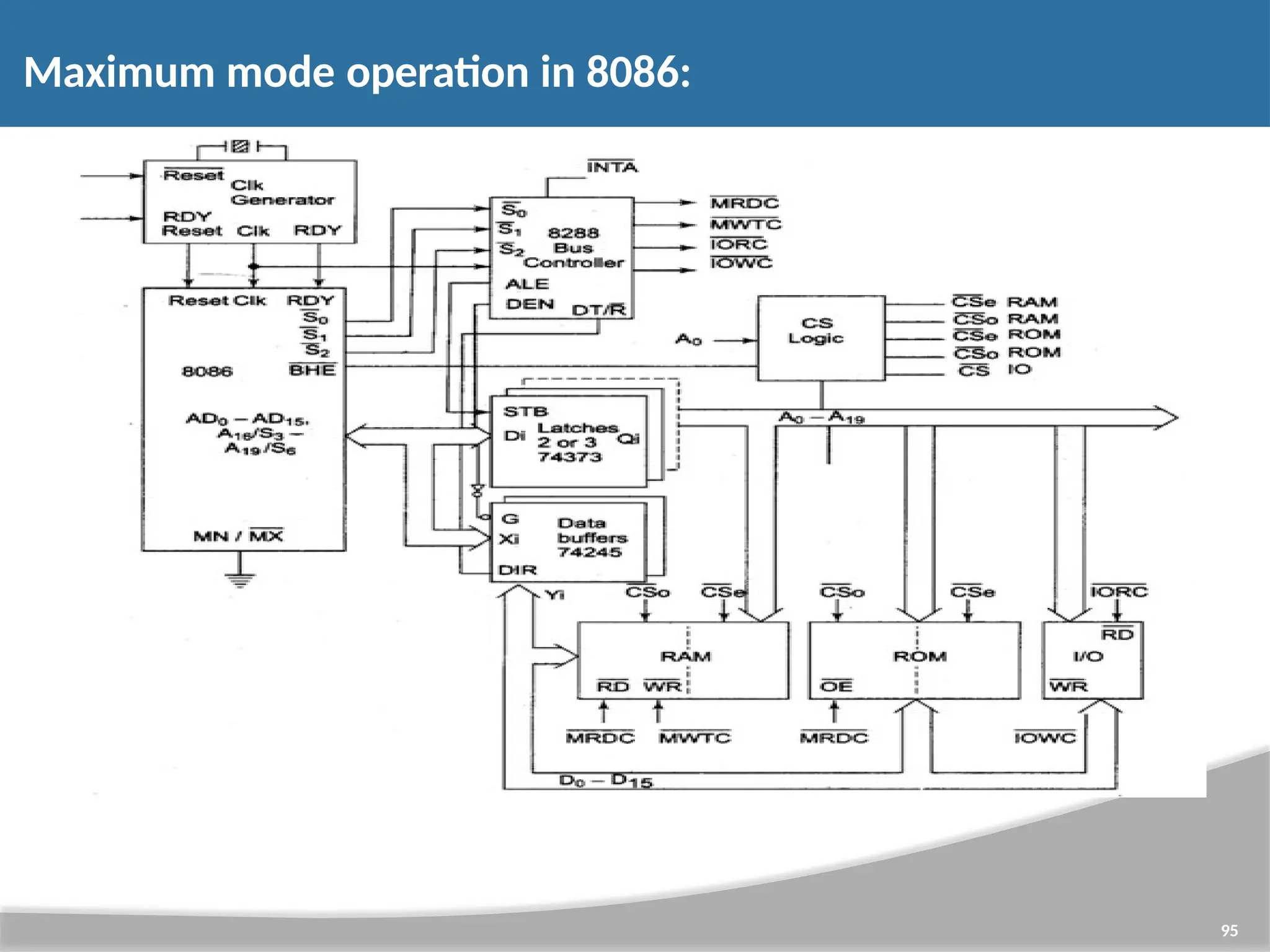
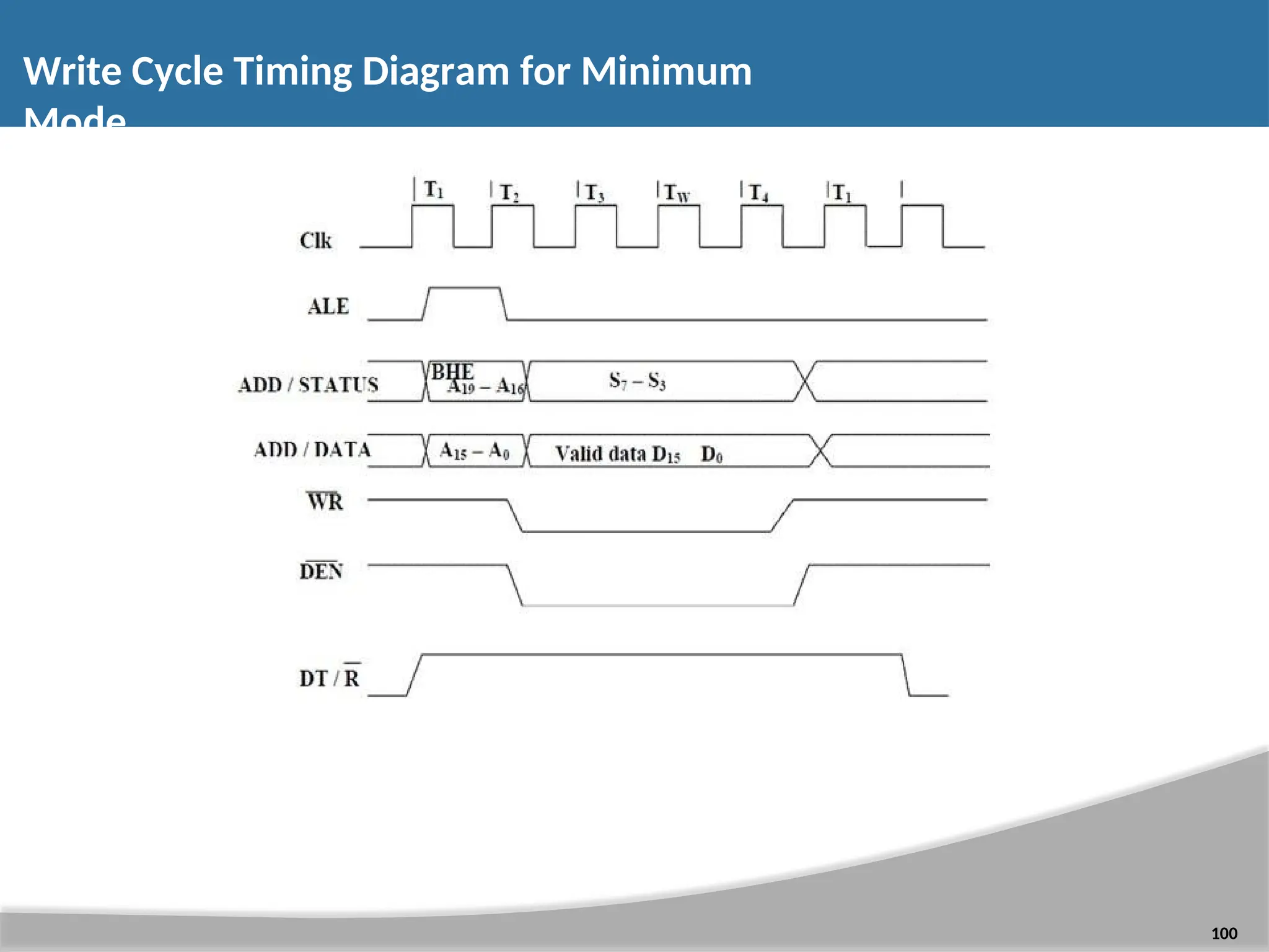
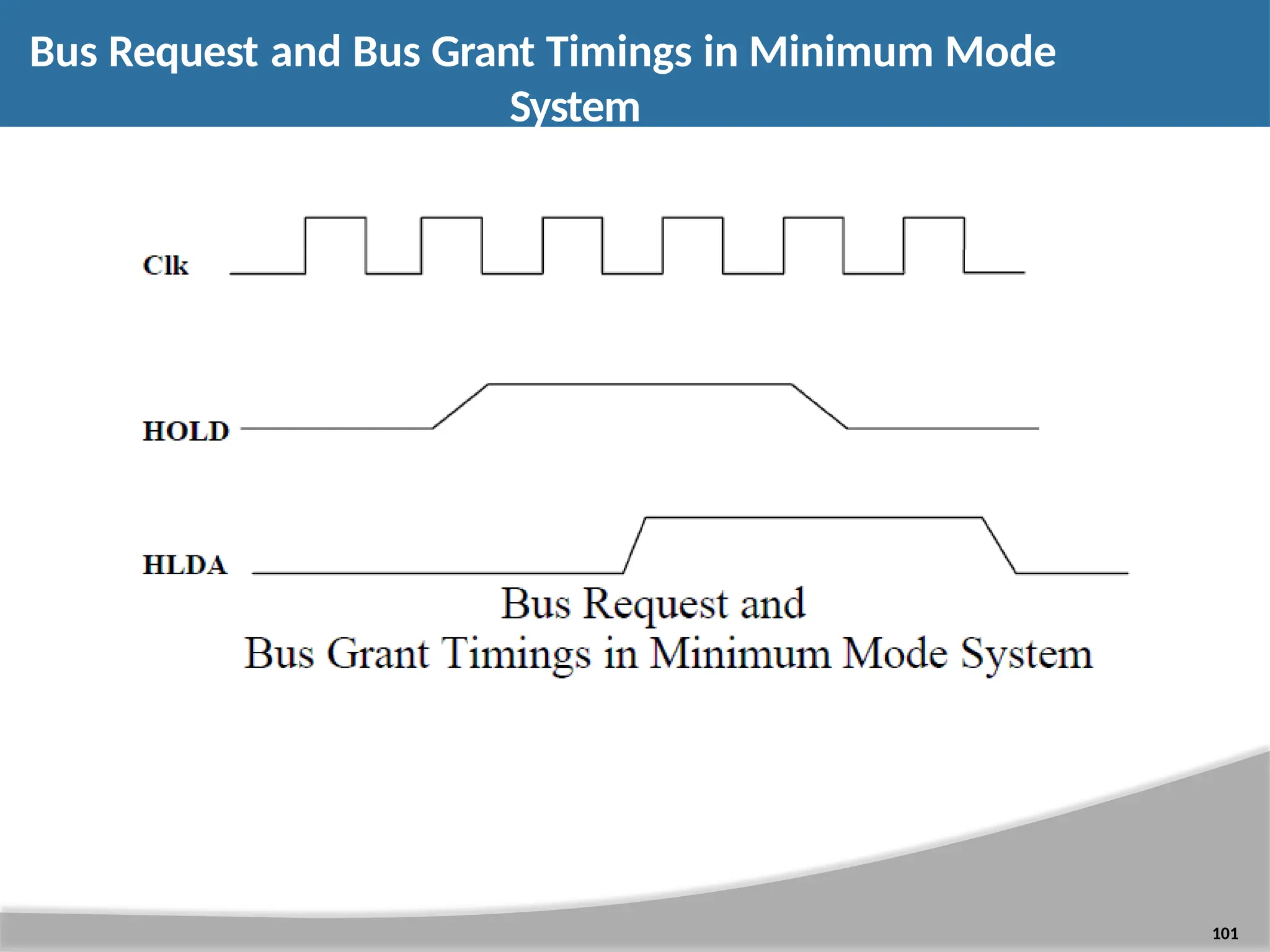
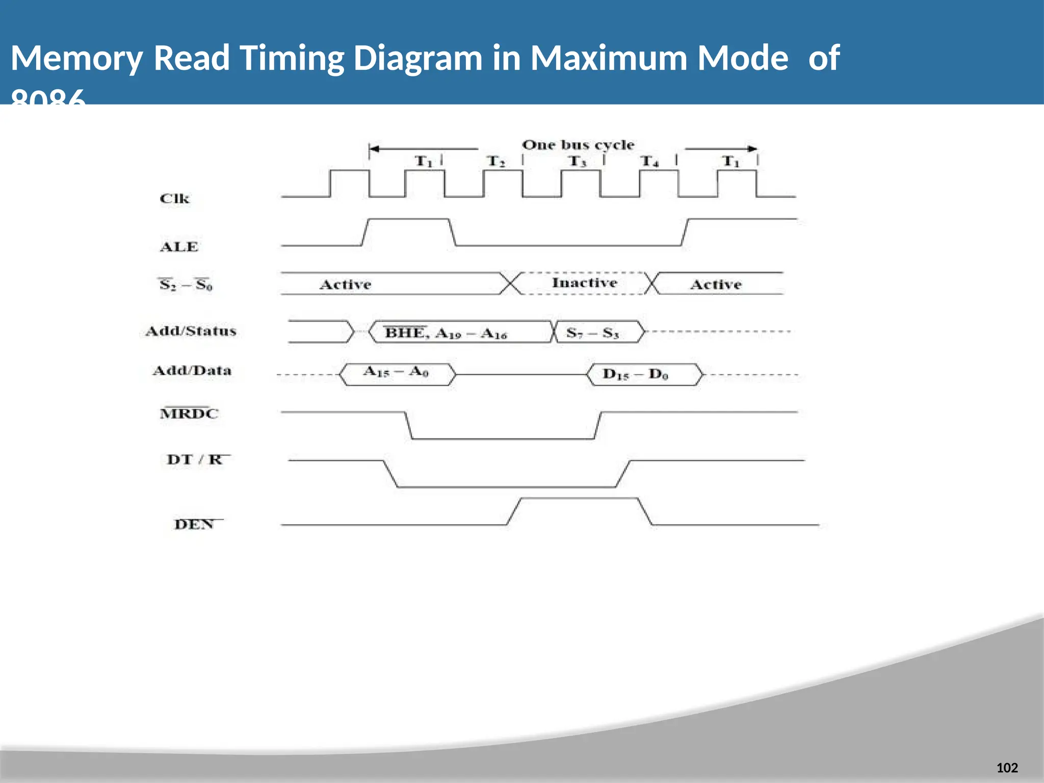
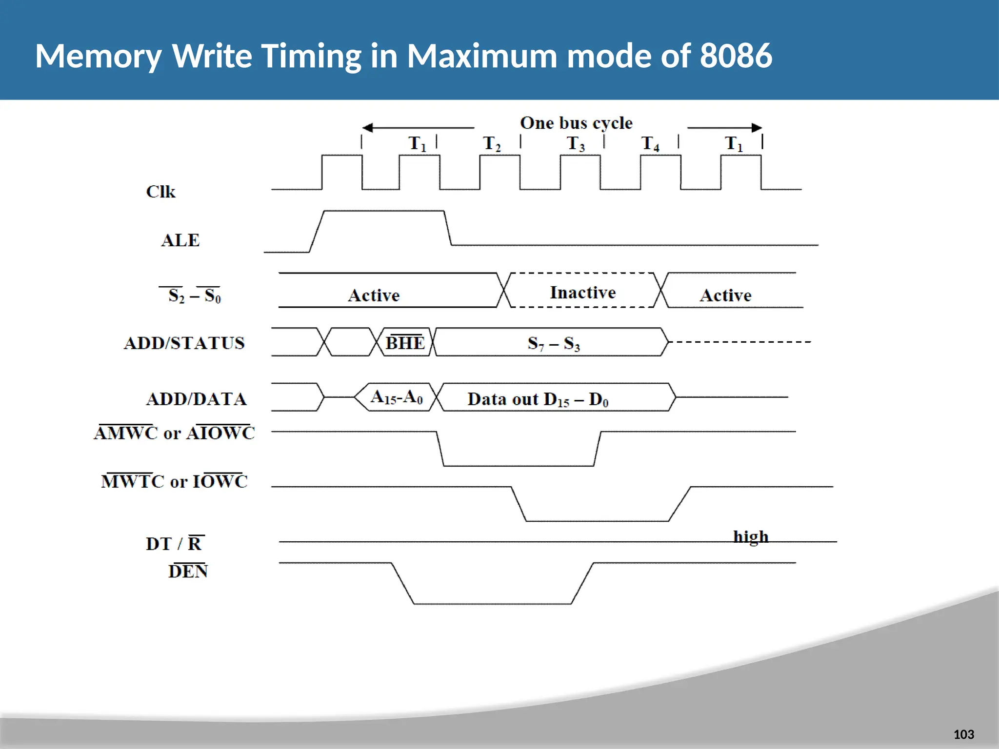
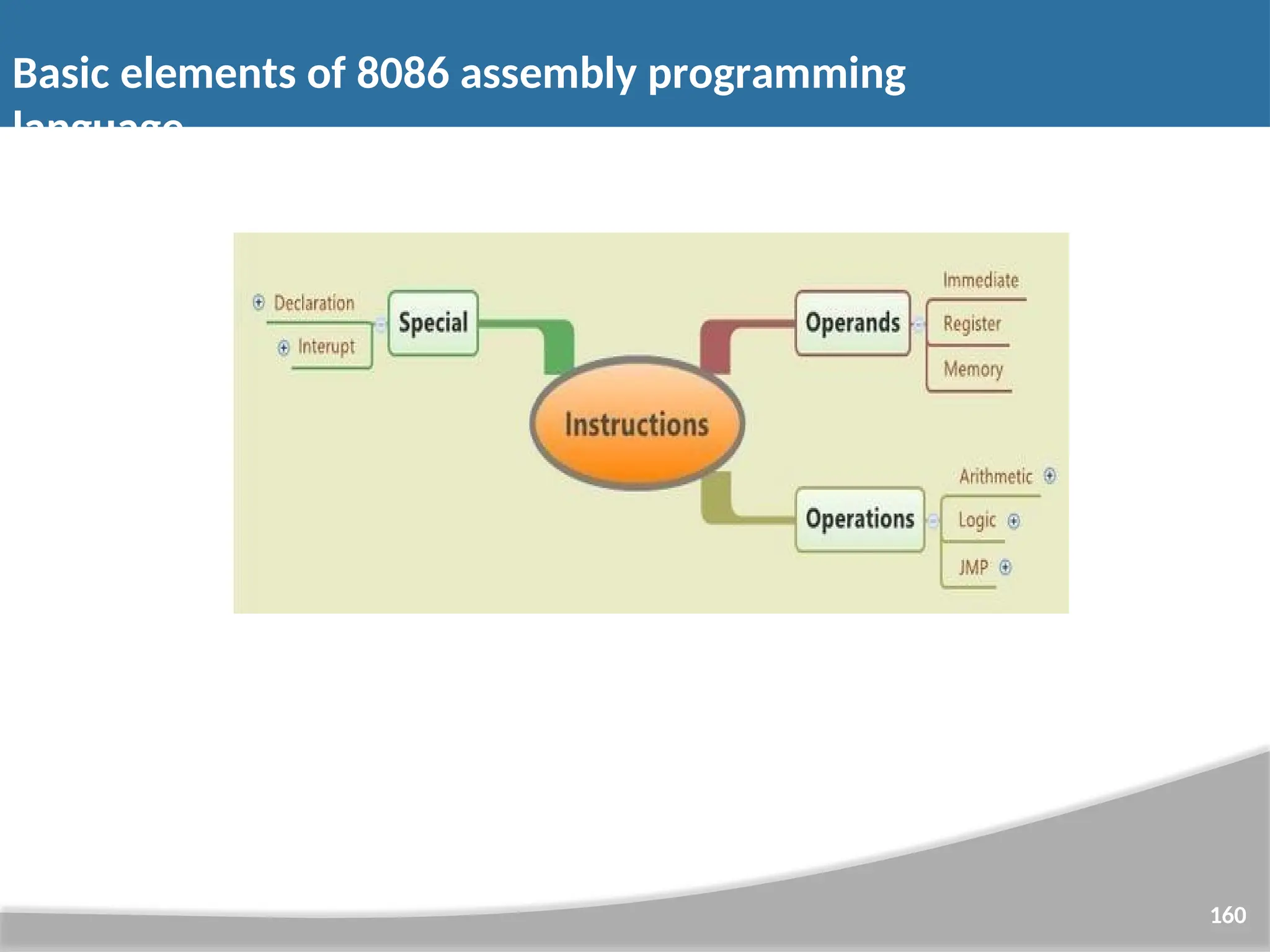
![8086 assembly programming language instructions 109 • Like we know instruction are the lines of a program that means an action for the computer to execute. In 8086, a normal instruction is made by an operation code and sometimes operands. Structure: Operation Code [Operand1 [, Operand2]] • Operations • The operation is usually logic or arithmetic, but we can also find some special operation like the Jump (JMP) operation.](https://image.slidesharecdn.com/mpmcppt1-250630101357-9236328f/75/Microprocessors-Microcontrollers-Architecture-and-Description-109-2048.jpg)