Bapuji Educational Association® BAPUJI INSTITUTE OF ENGINEERING AND TECHNOLOGY DAVANGERE, KARNATAKA-577004 DEPARTMENT OF ELECTRONICS & COMMUNICATION ENGINEERING Internship Progreess Presentation On “VLSI Design and Verification” Presented by, ABHISHEK S SHINGADI (4BD22EC400) Dr.G SUNITHA M.Tech. (DEAC), Ph.D., MISTE, FIETE., FIE Program Coordinator Dr. KIRAN KUMAR G H M.Tech. Ph.D. Internship Guide 1
2.
BAPUJI INSTITUTE OFENGINEERING AND TECHNOLOGY, DAVANGERE-577004 Vision To be a centre of excellence recognized nationally and internationally, in distinctive areas of engineering education and research, based on a culture of innovation and invention. Mission BIET contributes to the growth and development of its students by imparting a broad based engineering education and empowering them to be successful in their chosen field by inculcating in them positive approach, leadership qualities and ethical values. 2
3.
To be inthe forefront in providing quality technical education and research in Electronics & Communication Engineering to produce skilled professionals to cater to the challenges of the society. Mission of theDepartment M1: To facilitate the students with profound technical knowledge through effective teaching learning process for a successful career. M2: To impart quality education to strengthen students to meet the industry standards and face confidently the challenges in the programme. M3: To develop the essence of innovation and research among students and faculty by providing infrastructure and a conducive environment. M4: To inculcate the student community with ethical values, communication skills, leadership qualities, entrepreneurial skills and lifelong learning to meet the societal needs. Vision of the Department
4.
COURSE LEARNING OBJECTIVES Thiscourse will enable us to: 1. Experience a real-life engineering workplace and understand how their engineering knowledge and skills can be utilized in Industry. 2. Expose to the current Technological trends relevant to the field of training. 3. To enhance communication skills, teamwork capabilities and develop professional behaviour. 4. Use Internship experience to develop their engineering skills and practices that boost their employability. 5. Gain experience in writing technical/projects reports and expose students to the engineer’s responsibilities and ethics.
5.
Contents 1. Introduction 2. WORKCARRIED OUT IN FIRST WEEK 3. WORK CARRIED OUT IN SECOND WEEK 4. WORK CARRIED OUT IN THIRD WEEK 5. WORK CARRIED OUT IN FIRST WEEK
6.
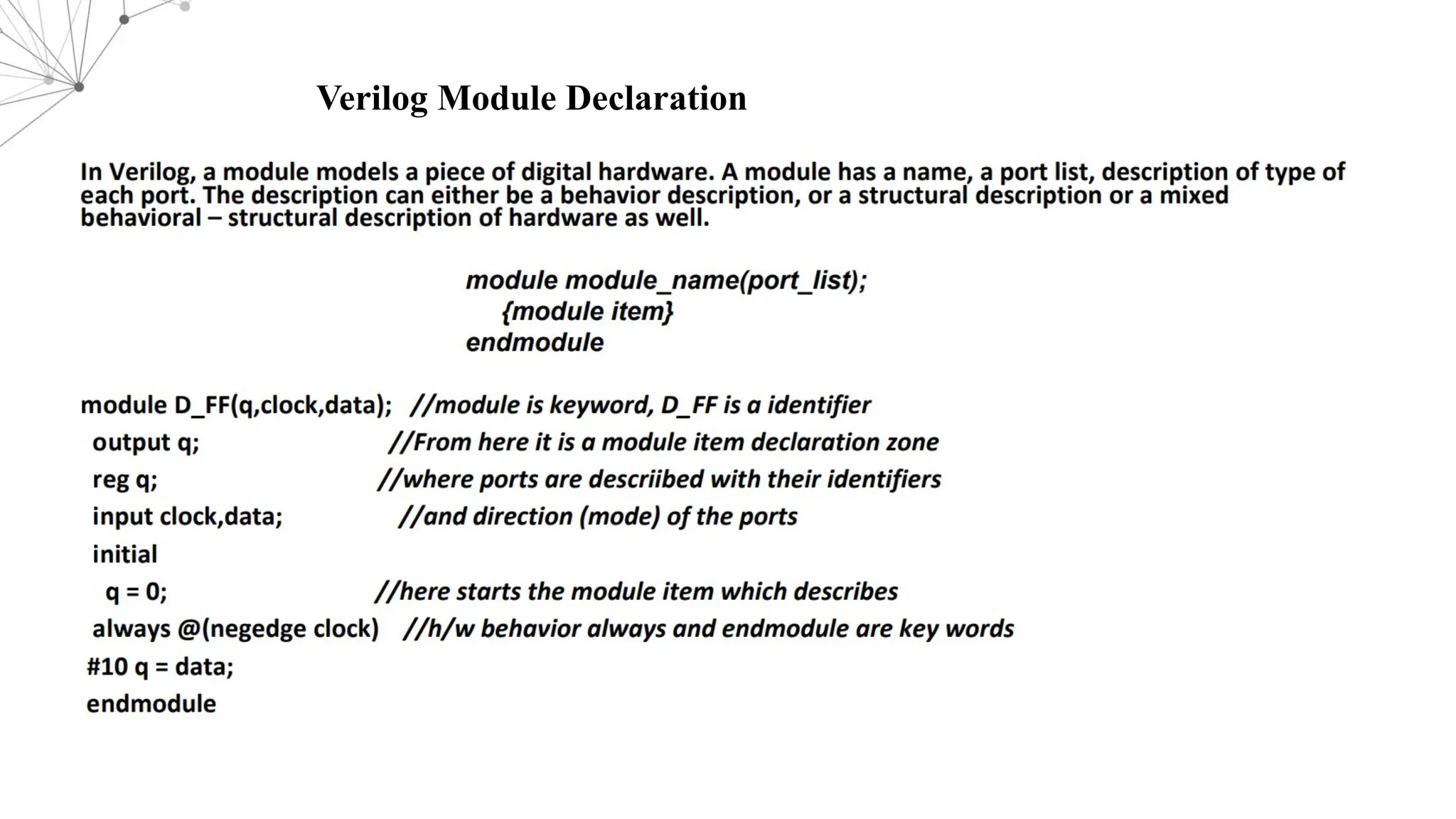
Introduction BASIC INFORMATION OFVERILOG ● Verilog is a hardware description language used for developing code that describes digital systems and circuits. ● For the design and verification of digital and mixed-signal systems, Verilog is frequently utilized including both application-specific integrated circuits (ASICs) and field-programmable gate arrays (FPGAs). ● Developed by Gateway Design Automation and later acquired by Cadence Design Systems
7.
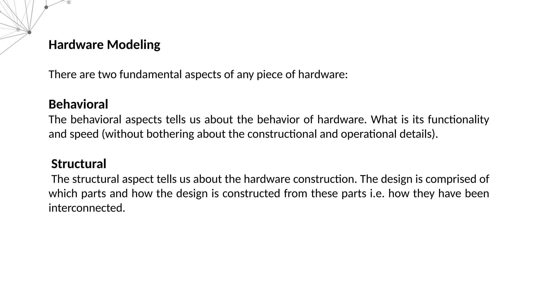
Hardware Modeling There aretwo fundamental aspects of any piece of hardware: Behavioral The behavioral aspects tells us about the behavior of hardware. What is its functionality and speed (without bothering about the constructional and operational details). Structural The structural aspect tells us about the hardware construction. The design is comprised of which parts and how the design is constructed from these parts i.e. how they have been interconnected.
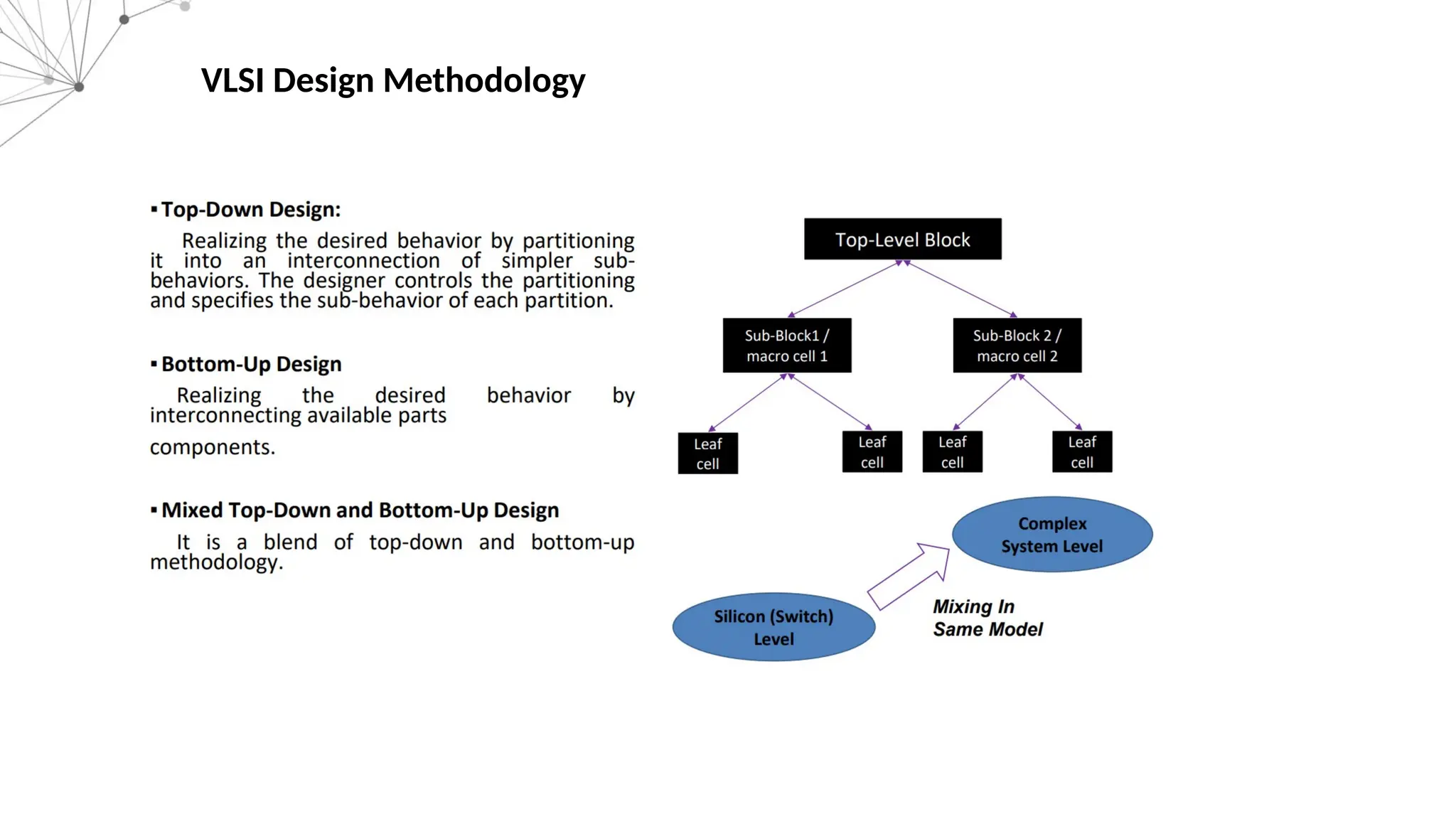
Modeling Styles Verilog isboth, behavioral and structural language. Designs in Verilog can be described at all the four levels of abstraction depending on needs of design. Behavioral Level: - Used to model behavior of design without concern for the hardware implementation details. Designing at this level is very similar to C programming. Dataflow Level [RTL]: - Module is specified by specifying the data flow. The designer is aware of how the data flows between registers. Gate Level: - Module is implemented in terms of logic gates & interconnections between them. Design at this level is similar to describing design in terms of gate level logical diagram. Switch Level: - lowest level of abstraction provided by Verilog. Module can be implemented in terms of switches, storage nodes & interconnection between them.
Gate Level HalfAdder Gate Level Half Adder Dataflow Level Half Adder Behavioral Level Half Adder / Adder Module module half_adder(sum,carry,A,B); output sum; output carry; input A, B; xor my_xor(sum,A,B); and my_and(carry,A,B); endmodule // Adder Module module half_adder(sum,carry,A,B); output sum; output carry; input A, B; assign sum = (~A&B) + (A&~B); assign carry = A&B; endmodule / Adder Module module half_adder(sum,carry,A,B); output sum; reg sum; output carry; reg carry; input A, B; always @(A or B) begin {carry, sum} = A + B; end endmodule
13.
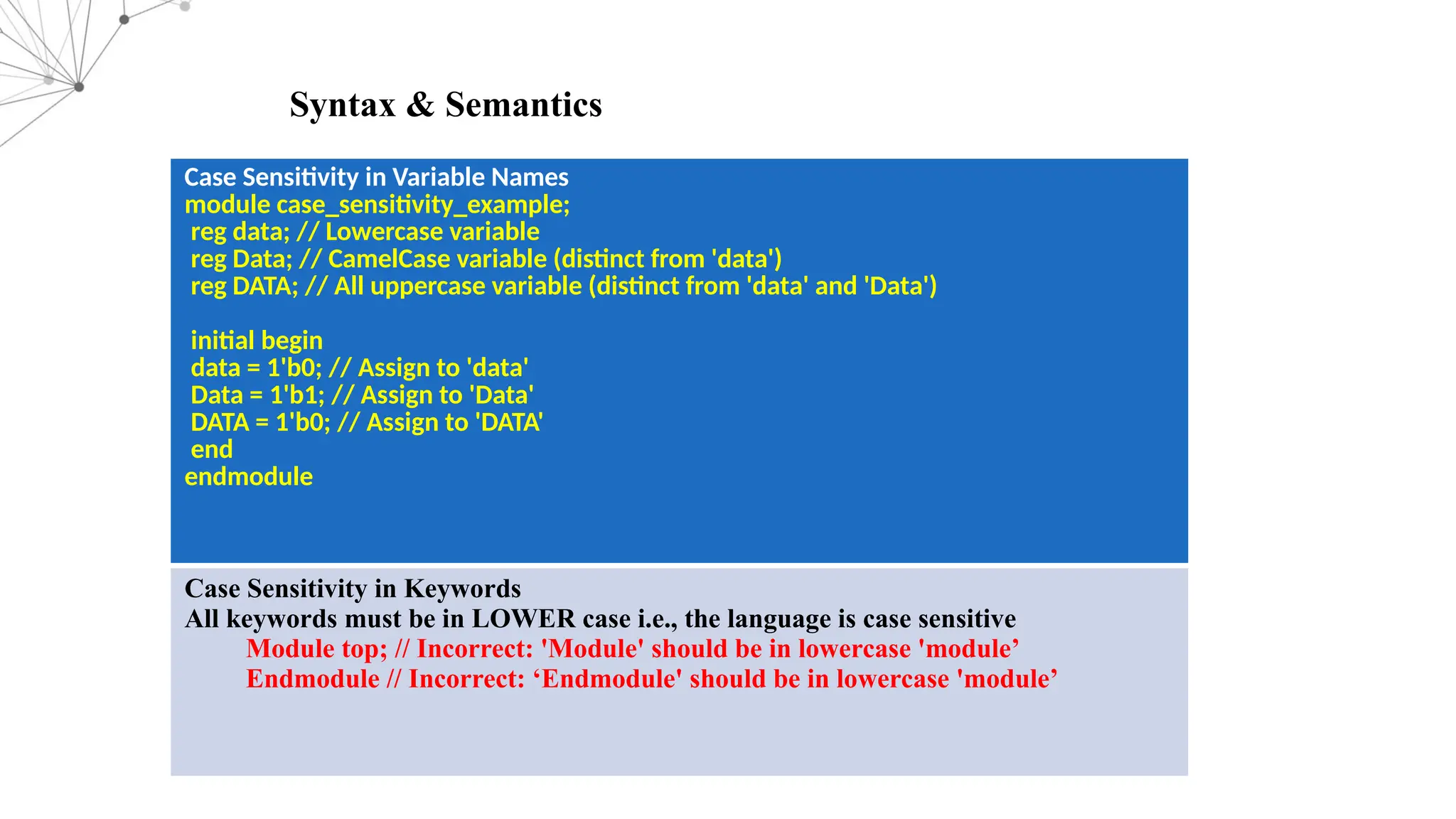
Case Sensitivity inVariable Names module case_sensitivity_example; reg data; // Lowercase variable reg Data; // CamelCase variable (distinct from 'data') reg DATA; // All uppercase variable (distinct from 'data' and 'Data') initial begin data = 1'b0; // Assign to 'data' Data = 1'b1; // Assign to 'Data' DATA = 1'b0; // Assign to 'DATA' end endmodule Case Sensitivity in Keywords All keywords must be in LOWER case i.e., the language is case sensitive Module top; // Incorrect: 'Module' should be in lowercase 'module’ Endmodule // Incorrect: ‘Endmodule' should be in lowercase 'module’ Syntax & Semantics
14.
VLSI Data Types 1.PhysicalData Types 2.Abstract (Register) Data Types 3.Constants 1.Physical Data Types ▪ “wor” performs “or” operation on multiple driver logic. E.g. ECL circuit ▪ “wand” performs “and” operation on multiple driver logic. E.g. Open collector output ▪ “trior” and “triand” perform the same function as “wor” and “wand”, but model outputs with resistive loads.
15.
2.Abstract (Register) DataTypes Vector:- A vector in Verilog is a collection of bits, and it can represent multi-bit signals such as buses or registers.. reg: {size = 1-bit, default value = 1’bx, type = unsigned} String:- there isn't a dedicated string data type for storing strings directly. However, you can use character arrays (or reg arrays) to store sequences of characters, which can be treated as strings. Each character can be stored as a single bit or a multi-bit representation, typically using 8 bits for ASCII characters Integer:- The integer data type in Verilog is used to represent signed integer values. It is a built-in data type that provides a way to store whole numbers, which can be both positive and negative. real:- The real data type is used to represent floating-point numbers, which can hold decimal values.
16.
3.Constants ▪ Constants canbe defined in a module by the keyword parameter. ▪ Thus, can not be used as variables. ▪ Improves code readability Parameter:- in Verilog. Parameters allow you to define constants that can be used throughout your module, making your code more flexible and easier to maintain. defparam:- The defparam statement in Verilog is used to override parameter values defined in a module instantiation. It allows you to specify different values for parameters at the time of module instantiation without modifying the original module.
17.
Gate level modellingand Concept Wire • Verilog language provides basic gates as built-in Primitives as shown. • Since they are predefined, they do not need module definition. • Primitives available in Verilog. i. Multiple input gates: and, nand, or, nor, xor, xnor ii. Multiple output gates: not,buf
18.
Continues Assignments andData Operators Syntax of assign statement: Assign < drive_strength > < delay > < list_of_assignment > input A, B, C; output Y; Assign Y = A & B Continuous assignment characteristics: • Left-Hand Side (LHS): Must be a net (like wire) or a combination of nets. Cannot be a register (like reg). • Right-Hand Side (RHS): Can be nets, registers, or function calls. Can be single bits (scalar) or multiple bits (vector). • Evaluation: The RHS expression is evaluated whenever any of its inputs change. The result is immediately assigned to the LHS. • Delays: You can add delays to control when the LHS gets the updated value.
19.
Verilog Data Operators:- ▪ Arithmetic ▪ Bitwise ▪ Logical ▪ Reduction ▪ Shift ▪ Relational ▪ Equality ▪ Concatenation ▪ Replication ▪ Conditional Arithmetic Operators ▪ If any operand contains z or x the result is unknown ▪ If result and operand are of same size, then carry is lost ▪ Treats vectors as a whole value Verilog Operators
20.
Bitwise Operators ▪ Operateson each bit of operand ▪ Result is in the size of the largest operand Logical Operators ▪ Can evaluate to 1, 0, x values ▪ The results is either true (1) or false (0) Shift Operators ▪ Shifts the bit of a vector left or right ▪ Shifted bits are lost ▪ Arithmetic shift right fills the shifted bits with sign bit ▪ All others fill the shifted bits by zero Operators Operations
21.
Relational Operators ▪ Evaluatesto 1, 0, x ▪ Result in x if any operand bit is z or x Equality Operators ▪ assign Write Me = (wr == 1) && ((a >= 16’h7000) && (a < 16’h8000));
22.
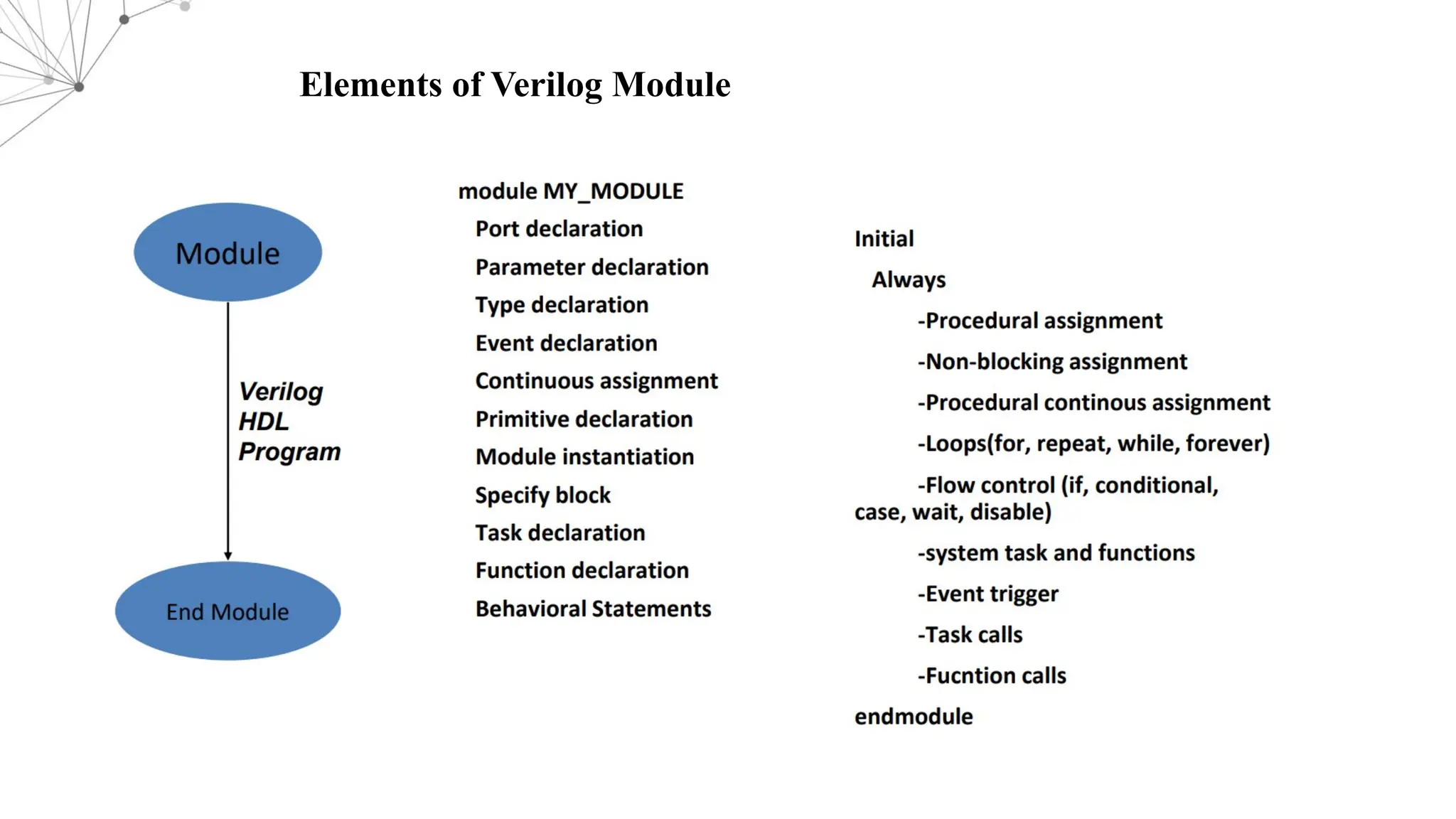
Procedural Blocks andAssignments in Verilog Always Block: Initial block is used in behavioral modeling to describe a block of code that runs only once at the beginning of the simulation. It’s often used to initialize values, generate stimulus, or set up certain conditions before the simulation runs. Initial Block: An always block in Verilog is used in behavioral modeling to describe behavior that should happen repeatedly, either based on a sensitivity list or at specified time intervals. It is typically used for modeling sequential logic, combinational logic, or clock-driven circuits. Procedural assignments: Procedural assignments are used within initial or always blocks to assign values to reg types. They allow you to model how the values of signals change over time, simulating the behavior of digital circuits. Non- blocking assignments: Non-blocking procedural assignments (<=) are commonly used in Verilog to model sequential logic, particularly when you want to simulate behavior similar to flip-flops or registers that store values on clock edges. Non-blocking assignments are designed to allow multiple assignments to be scheduled at the same time step without affecting the order of execution. Sequential Blocks: Statements are enclosed within the keywords begin & end. Statements are processed in order they are specified. Delays specified are additive Parallel Blocks:Statements are enclosed within the keywords fork & join. Statements in a parallel block are executed concurrently. Ordering of statements is controlled by the delay or event control assigned to each statement.
23.
▪ Timing Controls 1.Delay Based Timing Controls 2.Event Based Timing Controls 3. Level Sensitive Control 4.Conditional Statements -if...else/case
24.
1. Delay BasedTiming Controls Delay timing control types Declaration ▪ Regular delay control = The non-zero delay is specified at the LHS of the procedural statement. ▪ Intra-assignment delay control = Delay is specified between the assignment operator and the RHS operand. ▪ Zero delay control = The zero delay is specified at LHS of procedural statement 2.Event Based Timing Controls Event timing control types Declaration ▪ Regular event control = An event control is specified using @ symbol ▪ Event OR control = Multiple events are declared using the ‘or’ keyword or comma ‘,’ symbol. ▪ Named event control = The event declared using -> symbol as event triggering @ symbol as waiting for event trigger. ▪ Level sensitive timing control =The ‘wait’ keyword is used in the declaration
25.
3. Level SensitiveControl Along with the edge-sensitive construct (while waiting for an event trigger), Verilog adds up the ‘wait’ level-sensitive construct to wait for a specified condition to be true, and then only one or more statements will be executed. Thus, a set of statements will be blocked until the ‘wait’ condition is evaluated to be true. Syntax: wait(<expression or variable>) 4.Conditional Statements -if...else/case Verilog supports ‘if’, ‘else if’, ‘else’ same as other programming languages. The ‘If’ statement is a conditional statement based on which decision is made whether to execute lines inside if block or not. The begin and end are required in case of multiple lines present in ‘if’ block. For single-line inside if statement may not require ‘begin..end’ The ‘if’ statement returns true if the expression calculates its value as 1 otherwise, for 0, x, z values ‘if’ block will not be executed
26.
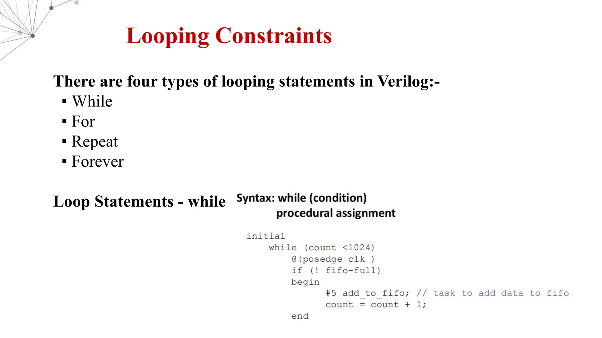
Looping Constraints There arefour types of looping statements in Verilog:- ▪ While ▪ For ▪ Repeat ▪ Forever Loop Statements - while
27.
Loop Statements -for Syntax: for (initial assignment; expression; step assignment) begin procedural assignment end
28.
Loop Statements -repeat ▪ Keyword repeat is used for this loop. ▪ Executes the loop for fixed number of times. Loop Statements - forever Looping statements appear inside procedural blocks only. The forever loop executes continuously i.e. the loop never ends
What is SystemVerilog? SystemVerilogis a hardware description and verification language (HDVL) that extends Verilog to support advanced modeling and verification of digital systems. It is widely used in designing and verifying Application-Specific Integrated Circuits (ASICs) and Field-Programmable Gate Arrays (FPGAs) Applications of SystemVerilog •Designing RTL (Register Transfer Level) Logic •Verification using Testbenches •Formal Property Checking and Coverage Analysis •Designing and Testing Complex Digital Systems (like CPUs, GPUs, and SoCs) SystemVerilog is standardized as IEEE 1800 and is widely supported by industry tool


![Modeling Styles Verilog is both, behavioral and structural language. Designs in Verilog can be described at all the four levels of abstraction depending on needs of design. Behavioral Level: - Used to model behavior of design without concern for the hardware implementation details. Designing at this level is very similar to C programming. Dataflow Level [RTL]: - Module is specified by specifying the data flow. The designer is aware of how the data flows between registers. Gate Level: - Module is implemented in terms of logic gates & interconnections between them. Design at this level is similar to describing design in terms of gate level logical diagram. Switch Level: - lowest level of abstraction provided by Verilog. Module can be implemented in terms of switches, storage nodes & interconnection between them.](https://image.slidesharecdn.com/internvlsi1-250304054102-ef846a16/75/INTERN-VLSI-1-pptx-INTERN-VLSI-1-pptx-ppt-9-2048.jpg)