Download to read offline
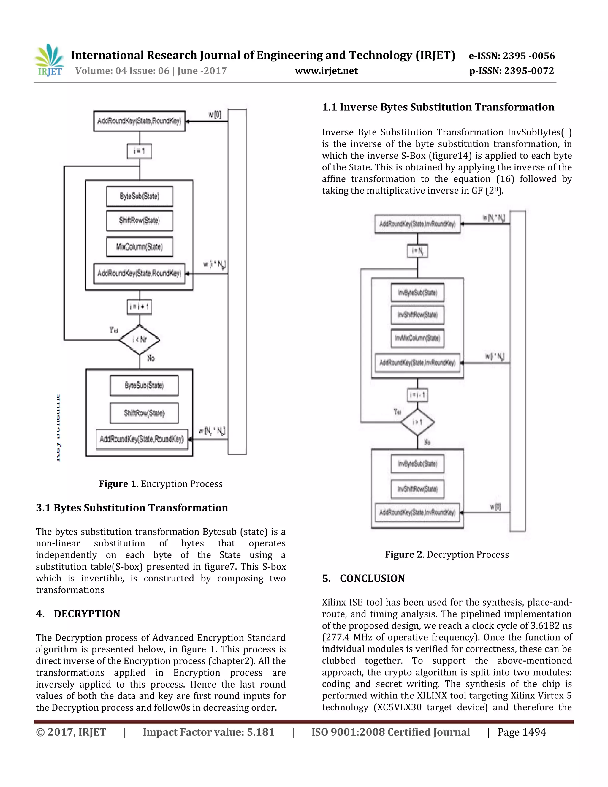
![International Research Journal of Engineering and Technology (IRJET) e-ISSN: 2395 -0056 Volume: 04 Issue: 06 | June -2017 www.irjet.net p-ISSN: 2395-0072 © 2017, IRJET | Impact Factor value: 5.181 | ISO 9001:2008 Certified Journal | Page 1493 HIGH SPEED OPTIMIZED AES USING PARALLEL PROCESSING IMPLEMENTATION R.Jerlin Emiliya1, D.Delphy2, B.Sangeetha3 1Associate professor hod of ece 2Assitant professor 3PG student, Dept. of ece, As Salam college of engg & tech, Tamil Nadu India --------------------------------------------------------------------***--------------------------------------------------------------------- Abstract - Advanced encryption standard (AES) algorithm has been widely deployed in cryptographic applications. This work proposes a low power and high throughput implementation of AES algorithm using key expansion approach. We minimize the power consumption and critical path delay using the proposed high performance architecture. It supports both encryption and decryption using 256-bitkeys with a throughput of 0.06 Gbps. The VHDL language is utilized for simulating the design and an FPGA chip has been used for the hardware implementations. Experimental results reveal that the proposed AES architectures offer superior performance than the existing VLSI architectures in terms of power, throughput and critical path delay. Key words: AES, VHDL, FPGA, Encryption, Decryption. 1. INTRODUCTION The recent years, there is a growing requirement to implement cryptographic algorithms in fast rising high- speed network applications. Encryption is the process of encoding information so that the unauthorized persons cannot identify the information. All the encryption algorithms convert the available information into unreadable secured form, referred to as cipher text. The authorized person will be able to decode the information using decryption algorithms. Two types of cryptographic systems available for data security are asymmetric (public- key) and symmetric (secret-keycryptographies (Hosseinkhani and Javadi, 2012). Asymmetric cryptography utilizes separate keys for encryption and encryption process for the key transportation mechanism. Conversely, symmetric cryptography utilizes an identical key for both encryption and decryption process, which is effective while handling a large amount of data (Chen et al.,2011). 2. LITERATURE SURVEY J. Daemen and V. Rijmen et al [1] Rijndael Algorithm is the importance of cryptography applied to security in electronic data transactions has acquired an essential relevance during the last few years. A VHDL- based implementation of the Advanced Encryption Standard (AES) algorithm is presented in this paper. The design has been coded by Very high speed integrated circuit Hardware Descriptive Language. All the results are synthesized using Xilinx ISE and simulated by using ModelSim software. Peter J. Ashenden et al [2] “The Designer's Guide to VHDL”, Advanced Encryption Standard can be programmed in software or built with pure hardware. This implementation is compared with other works to show the efficiency. All the transformations of both Encryptions and Decryption are simulated using an iterative design approach in order to minimize the hardware consumption. This research investigates the AES algorithm with regard to FPGA and the Very High Speed Integrated Circuit Hardware Description language (VHDL). Simulation results, performance results are presented and compared with previous reported designs. 3. ENCRYPTION The Encryption process of Advanced Encryption Standard algorithm is presented below, in figure 1. This block diagram is generic for AES specifications. It consists of a number of different transformations applied consecutively over the data block bits, in a fixed number of iterations, called rounds. The number of rounds depends on the length of the key used for the encryption process.](https://image.slidesharecdn.com/irjet-v4i6278-180201105013/75/High-Speed-Optimized-AES-using-Parallel-Processing-Implementation-1-2048.jpg)
![International Research Journal of Engineering and Technology (IRJET) e-ISSN: 2395 -0056 Volume: 04 Issue: 06 | June -2017 www.irjet.net p-ISSN: 2395-0072 © 2017, IRJET | Impact Factor value: 5.181 | ISO 9001:2008 Certified Journal | Page 1495 report is given in Table 1. The combination of Modelsim and Xilinx design flow has been used for the entire process. Individual register transfer logic (RTL) is obtained once synthesizing the VHDL style. The timing simulation is additionally performed to verify the functional correctness of the planning. However, the RTL diagram is not enclosed here for conciseness. The power analysis is performed using Xilinx’s XPower analysis tool. The Virtex 5 Pro is a target device, as it is a full featured and flexible FPGA that contains two Power PC cores and plenty of logic cells and Devices, Figure 3. Simulation Result. Figure 4. Device Utilization I/O pin counts ranging from 208 to 1164 (Xilinx). It is set to run at 25 MHz during the simulations. Fig. 3 shows the simulation result forth encryption of a test vector. The design is synthesized in Xilinx Environment. The target device is xc5vlx30 in the family of Virtex5.Through the analysis of the schemes for throughput and power, it is evident that the proposed scheme outperforms the existing schemes. The standard national institute of standards and technology (NIST) and direct optimized routing(DOR) methodologies have been compared with the proposed technique. Table 2 compares the critical path, throughput, and power of the proposed technique with NIST and DOR techniques. The throughput of the DOR scheme is more comparing to the NIST scheme at the cost double number of required LUT slices for implementation. However, the proposed scheme provides the highest throughput of 277.4 Mbps with 31.8% reduction respectively in the LUT slices. REFERENCES [1] FIPS 197, “Advanced Encryption Standard (AES)”, November 26, 2001 [2] J. Daemen and V. Rijmen, “AES Proposal: Rijndael”, AES Algorithm Submission, September 3, 1999 [3] ALTERA. Max+plus II VHDL. San Jose. Altera, 1996 [4] ALTERA “ACEX1K Embedded Programmable Logic Family Data Sheet”, pdf files, (May 2003) [5] ALTERA High-Speed RijndaelEncryption / Decryption Processors, [6] Marcelo B. de Barcelos Design Case, “Optimized performance and area implementation of Advanced Encryption Standard in Altera [7] “FPGA Simulations of Round 2 Advanced Encryption Standards” [8] Tilborg, Henk C. A. van. “Fundamentals of Cryptology: A Professional Reference and Interactive Tutorial”, New York Kluwer Academic Publishers, 2002 [9] Peter J. Ashenden, “The Designer's Guide to VHDL”, 2nd Edition, San Francisco, CA, Morgan Kaufmann, 2002](https://image.slidesharecdn.com/irjet-v4i6278-180201105013/75/High-Speed-Optimized-AES-using-Parallel-Processing-Implementation-3-2048.jpg)

This document presents a proposed optimized implementation of the Advanced Encryption Standard (AES) algorithm using parallel processing for high-speed encryption and decryption. The implementation aims to minimize power consumption and critical path delay. It was designed and simulated using VHDL and implemented on an FPGA chip. Experimental results showed that the proposed AES architecture offers superior performance to existing VLSI architectures in terms of power, throughput, and critical path delay. The architecture supports encryption and decryption of 256-bit keys with a throughput of 0.06 Gbps.