Downloaded 275 times


This document provides an overview of Field Programmable Gate Arrays (FPGAs). It discusses that FPGAs are programmable logic devices with a 2D array of logic blocks and flip-flops that can be configured by the user. The document outlines the core components of an FPGA including logic blocks, look-up tables, multiplexers, flip-flops, and programmable interconnections. It also describes different FPGA programming technologies such as SRAM, antifuse, EPROM, and EEPROM programming. The document concludes by discussing FPGA advantages such as rapid prototyping and reconfigurability compared to ASICs.
Presented by Srishti Jain from V semester.
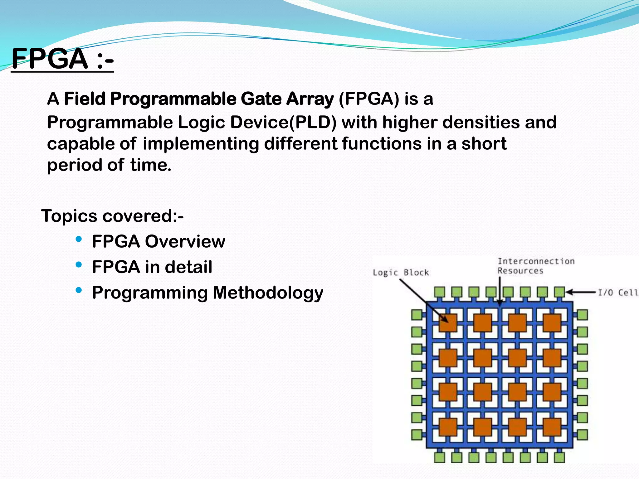
FPGA is a programmable logic device. Covers overview, in-depth detail, and programming methodology.
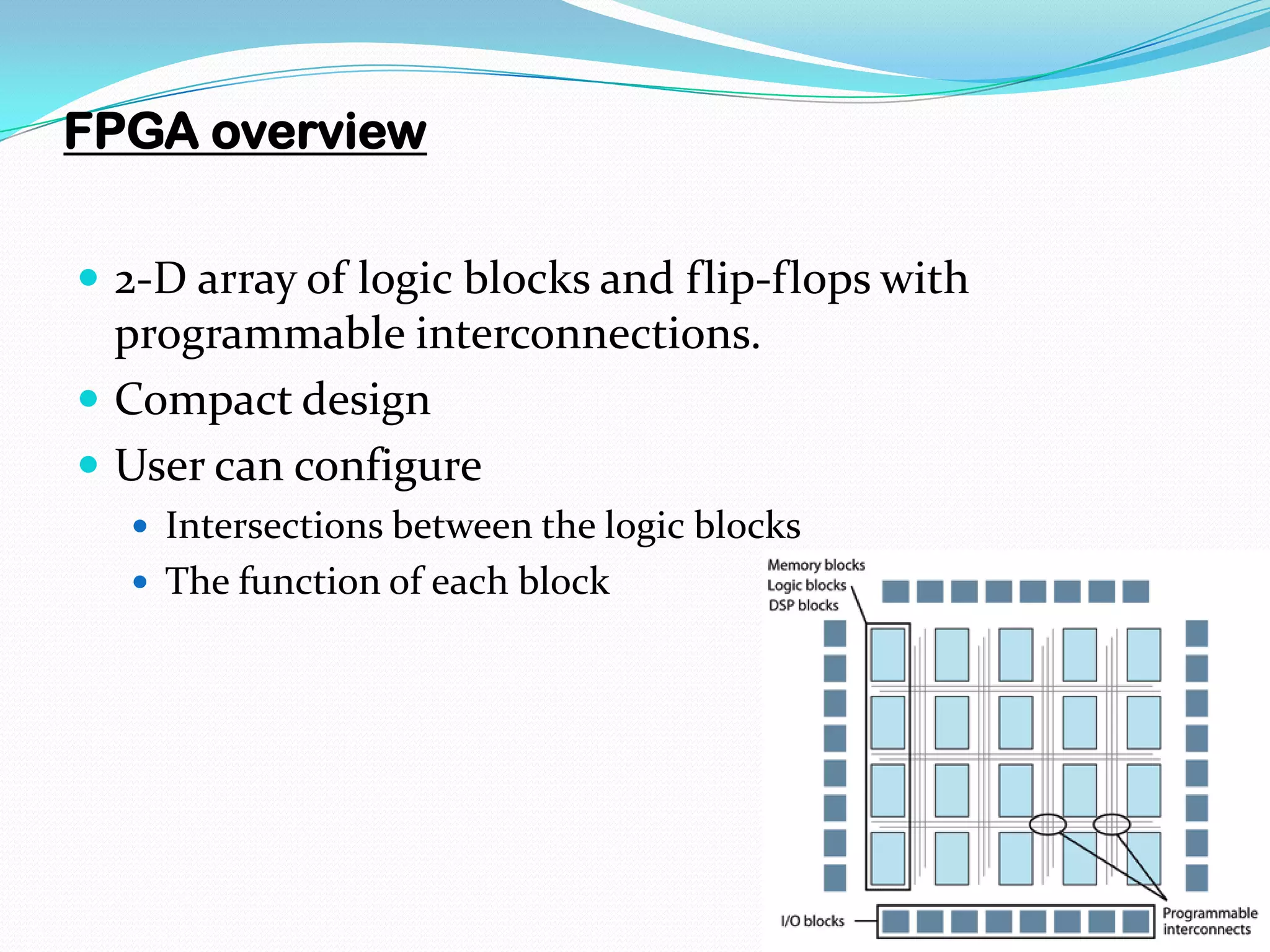
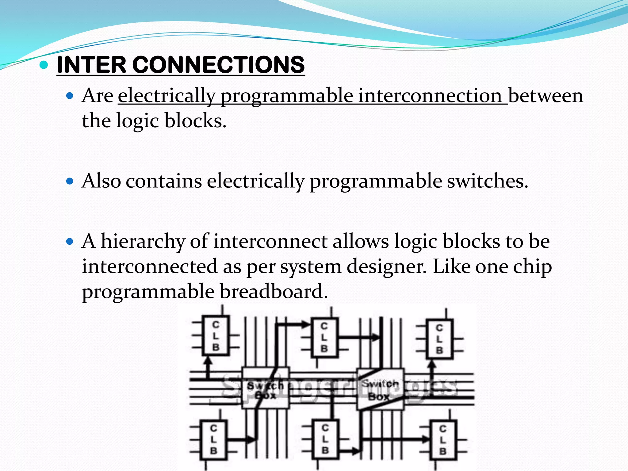
FPGA consists of a 2-D array of logic blocks and flip-flops with programmable interconnections.
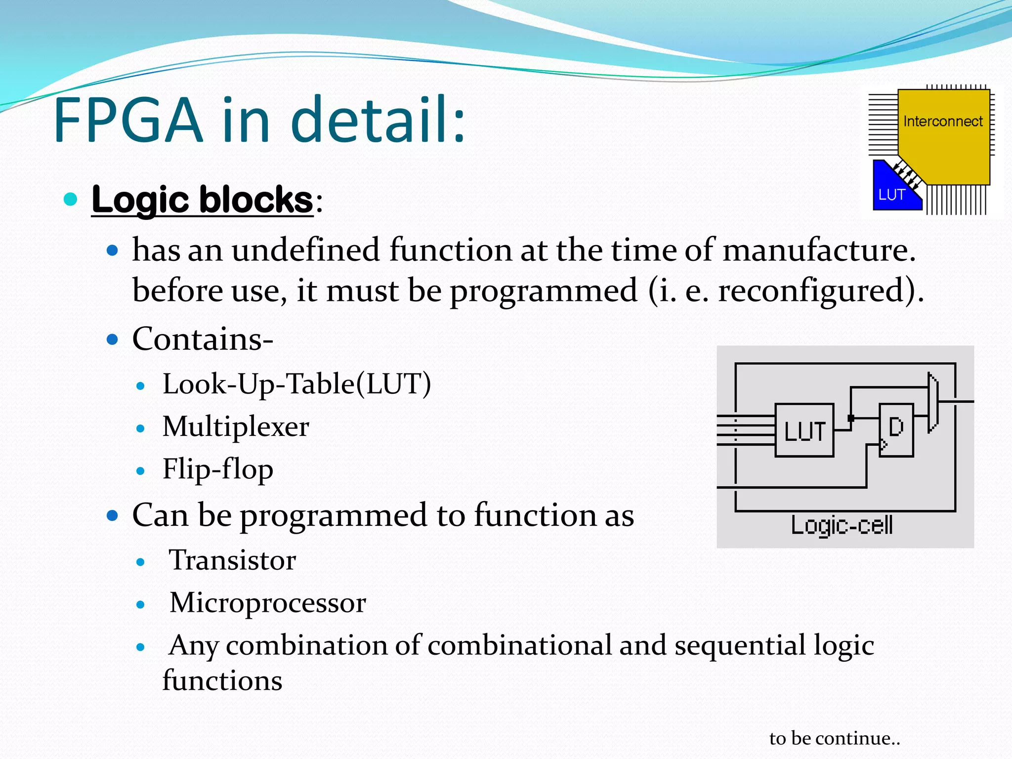
Logic blocks can be programmed for various functions, containing LUTs, multiplexers, and flip-flops.
Electrically programmable interconnections allow user-defined connections between logic blocks.
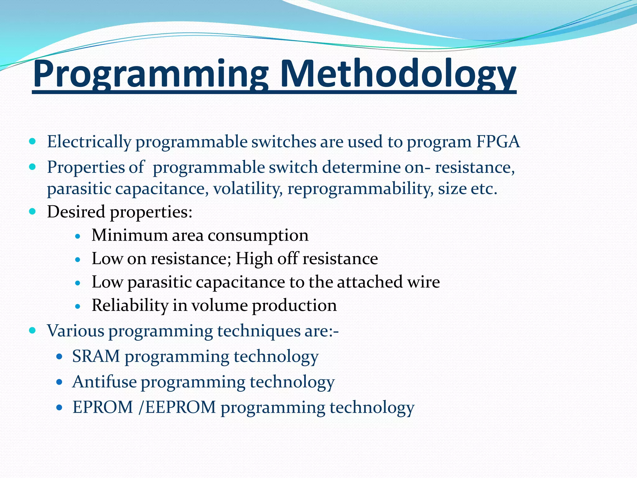
Programming methodology involves switch properties and techniques such as SRAM, antifuse, and EPROM.
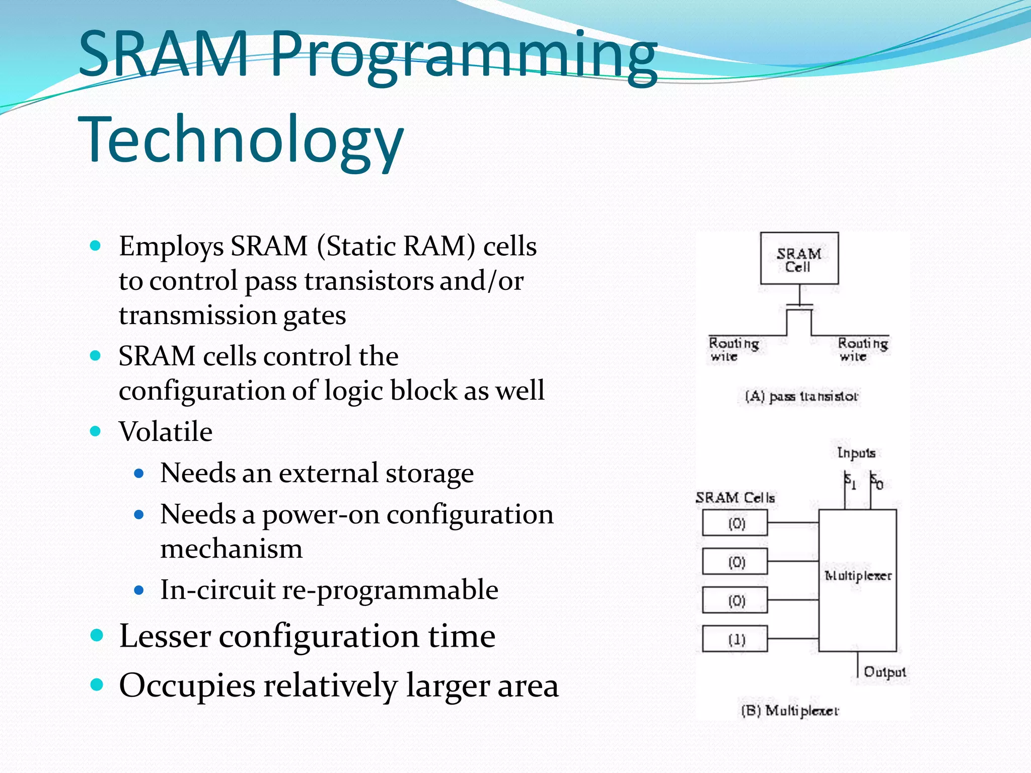
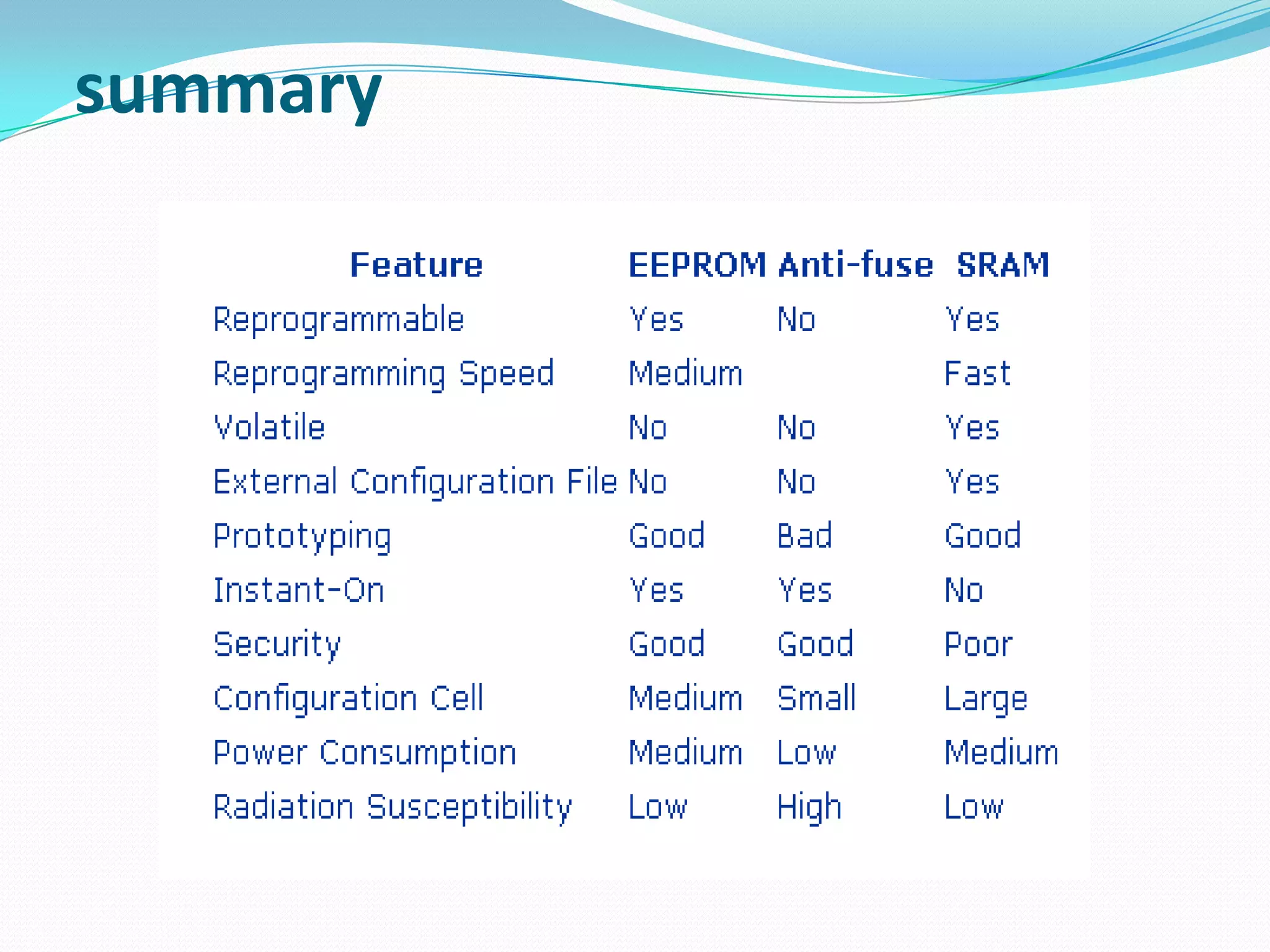
SRAM uses volatile memory to control logic block configurations; it is re-programmable but occupies larger areas.
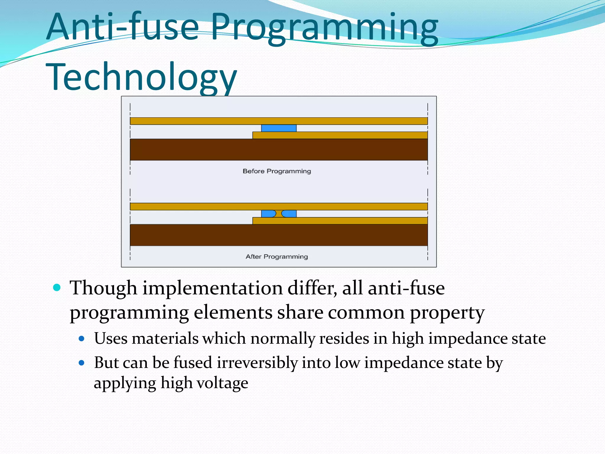
Anti-fuse programming is one-time programmable, offers low resistance, and retains configuration after power off.
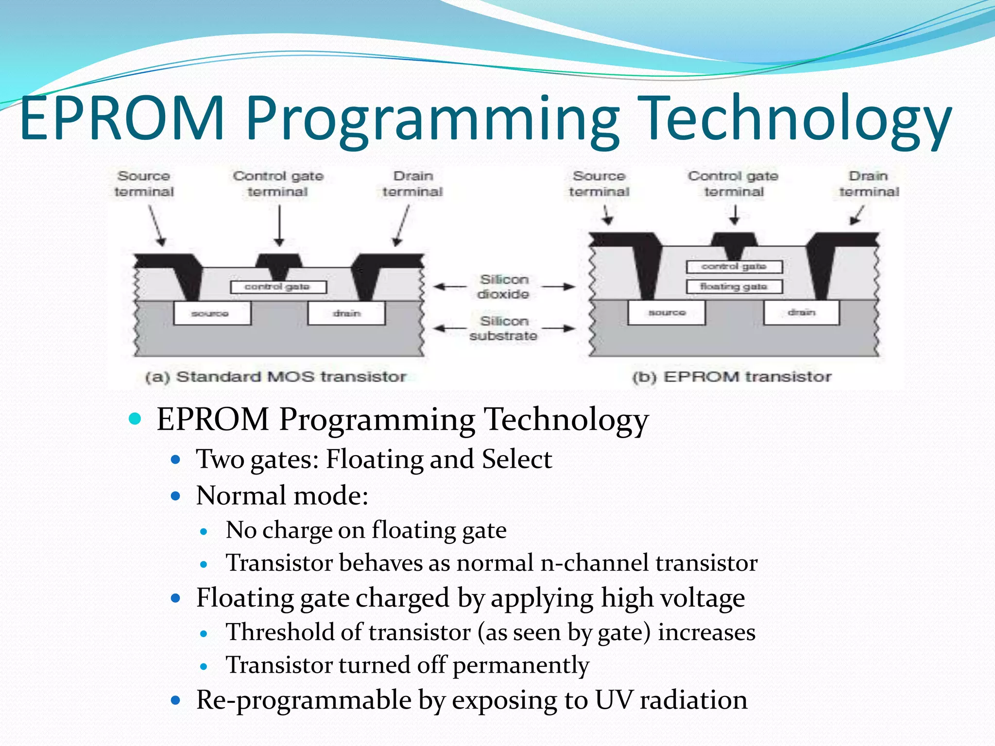
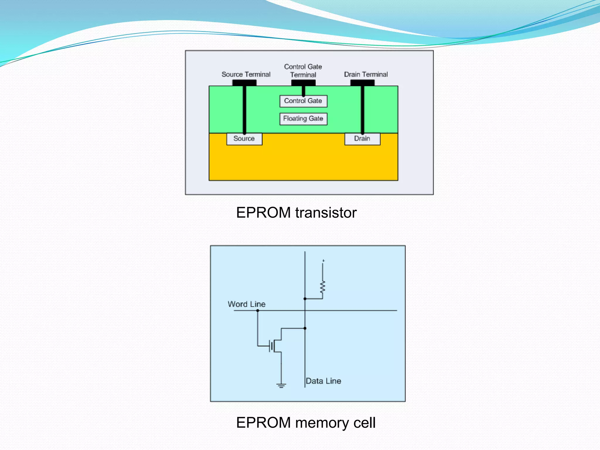
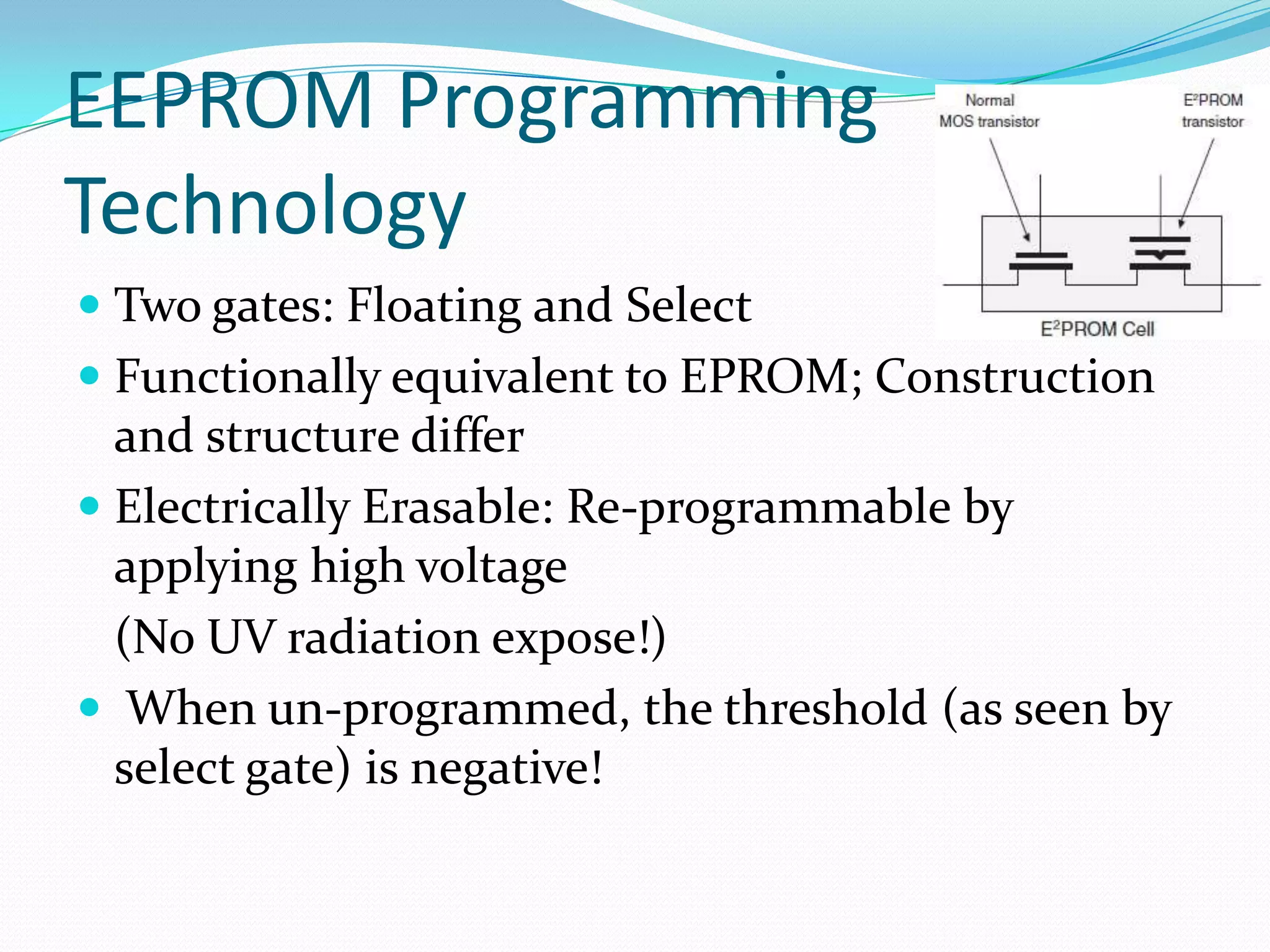
EPROM uses high voltage for programming and can be re-programmed using UV radiation; not in-system re-programmable.
EEPROM can be re-programmed electrically without UV radiation; offers convenience in erasing cells.
FPGAs provide rapid prototyping, easy upgrades, and have lower manufacturing costs compared to ASIC.
FPGAs allow for quicker debugging and modifications but are generally slower and power-consuming than ASIC.
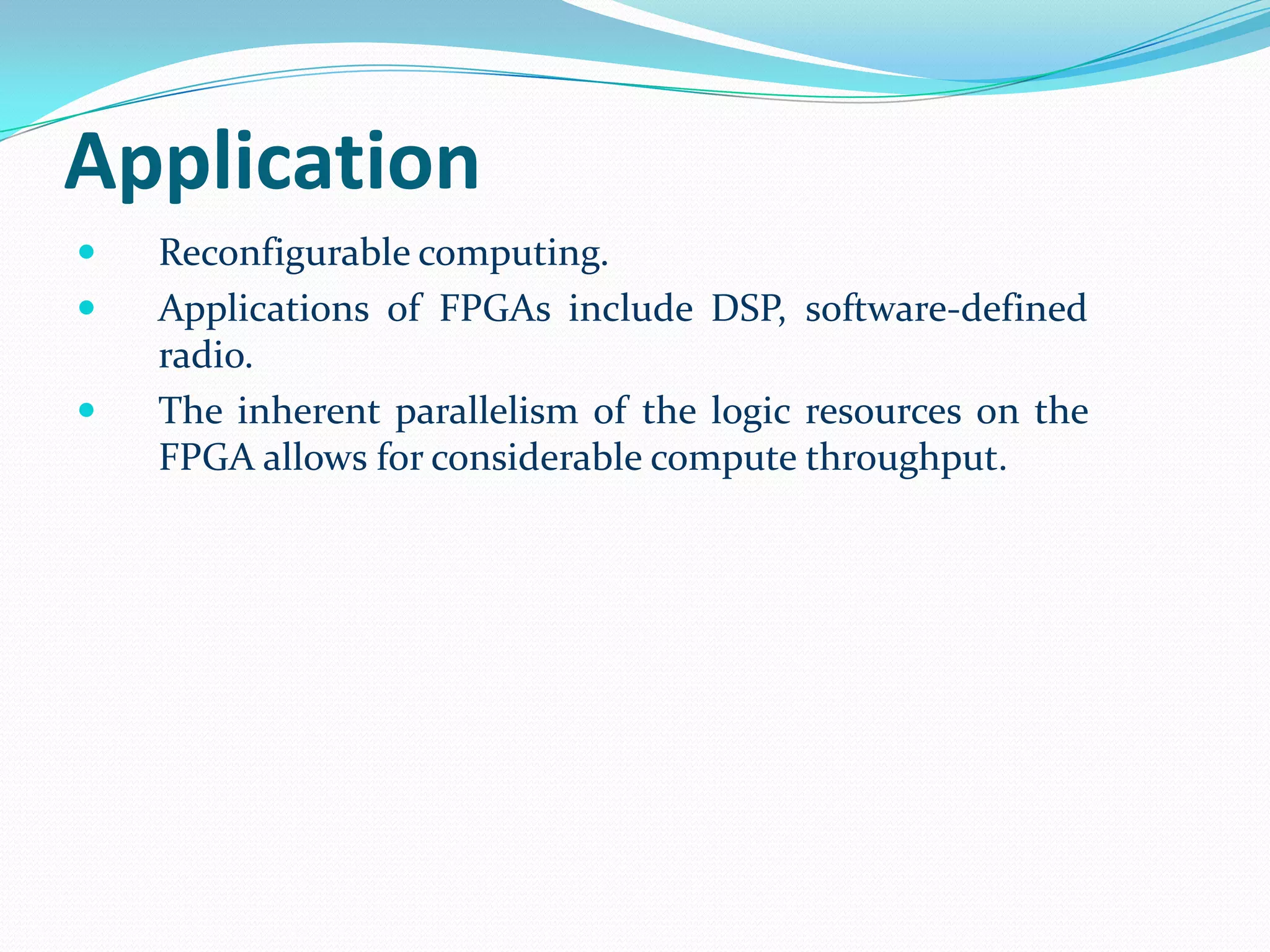
Applications include reconfigurable computing in areas like DSP and software-defined radio.
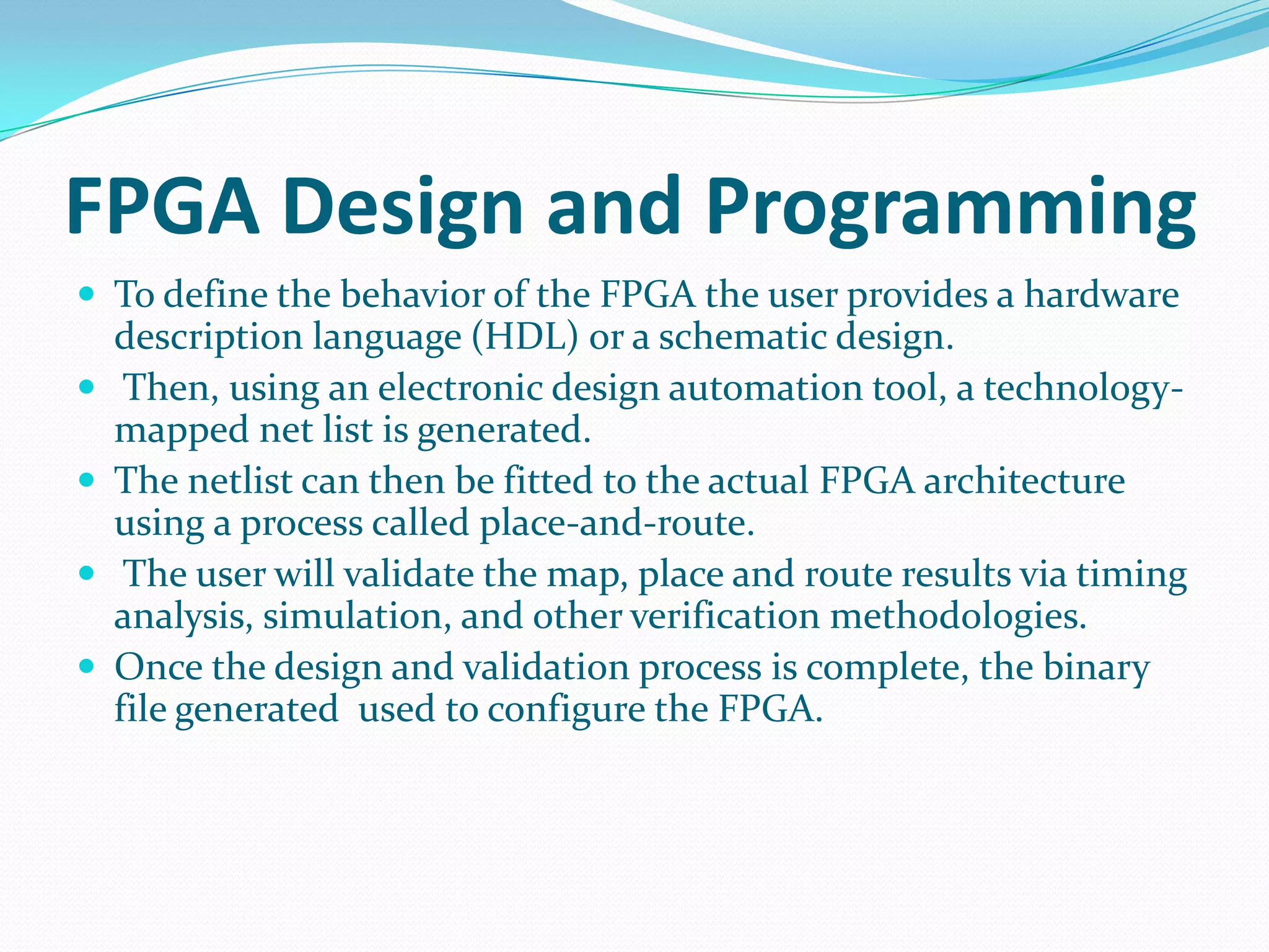
Design process involves HDL input, netlist generation, and validation through various methods.
Thank you for attending the presentation on FPGA.