Download to read offline
![Bhuvaneswari .S, Prabakaran .R, Muniraj N. J. R, International Journal of Advance Research, Ideas and Innovations in Technology. © 2017, www.IJARIIT.com All Rights Reserved Page | 140 ISSN: 2454-132X Impact factor: 4.295 (Volume3, Issue6) Available online at www.ijariit.com Efficient Implementation of 2-Bit Magnitude Comparator Using PTL S. Bhuvaneswari PG Scholar, Department Of ECE Tejaa Shakthi Institute of Technology for Women, Coimbatore, Tamil Nadu sayhaitosbspinky@gmail.com R. Prabakaran Assistant Professor, Department Of ECE Tejaa Shakthi Institute of Technology for Women, Coimbatore, Tamil Nadu prabakaranto@gmail.com Dr. N. J. R Muniraj Principal, Department Of ECE Tejaa Shakthi Institute of Technology for Women, Coimbatore, Tamil Nadu njrmuniraj@yahoo.co.in Abstract: Nowadays the requirements of low power electronics play a vital role in various fields. In this paper we introducing the novel comparator is one of the fundamental units in VLSI design and also it can be employed in various applications like Digital Signal Processors (DSP) and Data Processing, Communication Systems, Medical Electronics etc., Comparator is involved to the most basic arithmetic operation of compression between any two variables either it maybe an equal one or unequal. In early days, the comparator techniques used to implement energy optimization in low power circuits but the static power dissipation need to improve the comparator using logic styles. In this paper, the 2-bit comparator has been designed by using pass transistor logic (PTL). PTL provide good performance by reducing transistor count as well as power because PTL logic helps in reducing the transistor count compared to other logic operation. The design was implemented in Cadence virtuoso TMSC 180nm CMOS technology and it’s obtaining the total power dissipation 1.394µw. PTL logic is used to reduce both transistor count and power dissipation in magnitude comparator is used to improve the good quality performance of this circuit. Keywords: CMOS, Magnitude Comparator, Logic Gates, Pass Transistor Logic. I. INTRODUCTION In comparator circuit design, the CMOS technology has a central position in modern designing methodology. The comparator is one of the fundamental units which have extensive application areas in VLSI systems such as CPU, decoding of microprocessor instructions. The comparator is well known to be a very basic and useful component of arithmetic units of the digital systems. In such systems, comparison of any two numbers is said to be a necessary arithmetic operation that determines whether a number is greater than, equal to, or less than the other number. Magnitude comparator forms a combinational circuit to compare two numbers, let A and B, and finally determine their relative magnitudes and thereby relation between the two equal to, less than, greater than. The comparator has a very useful component in many areas such as multi-access memories, parallel computing and multiprocessing [1]. Here we can use various type of logic styles are used such as CMOS logic styles, transmission gate logic styles, pass transistor logic styles etc., PTL Logic Style provides less PDP as compared to another logic style. It has been found that transistor count is less in PTL style design than that of other logic style design [2]. Design and implementation of the full adder circuit, using Transmission Gates and multiplexers in order to reduce transistor count. The full adder using 27 transistors designed as very high power consumption and increases the number of the transistor. To overcome this problem full adder using 18 transistors to reduces power and area [3]. Different VLSI scaling methods are used to reduce the power dissipation. The scaling method is voltage scaling, load scaling is to increase the power dissipation. Low power transmission gate (LPTG) buffer are used to reduce the leakage current and power dissipation [4]. The buffer consists of a chain of inverter stages where the width of each MOS transistor in a stage is increased by a constant factor than the previous stage. The taper buffer design provides 15% reduction in power dissipation at the same value of propagation delay when compared with the conventional design [5]. Scaling methods improves transistor density and functionality on a chip. Scaling helps to increase speed and frequency of operation and hence higher performance [6]. The comparator is based on another logic style of a full adder. The full adder circuit is basically designed by using X-OR gate and 2:1 MUX.](https://image.slidesharecdn.com/efficientimplementationof2-bitmagnitudecomparatorusingpt-180109055318/75/Efficient-implementation-of-2-bit-magnitude-comparator-using-pt-1-2048.jpg)
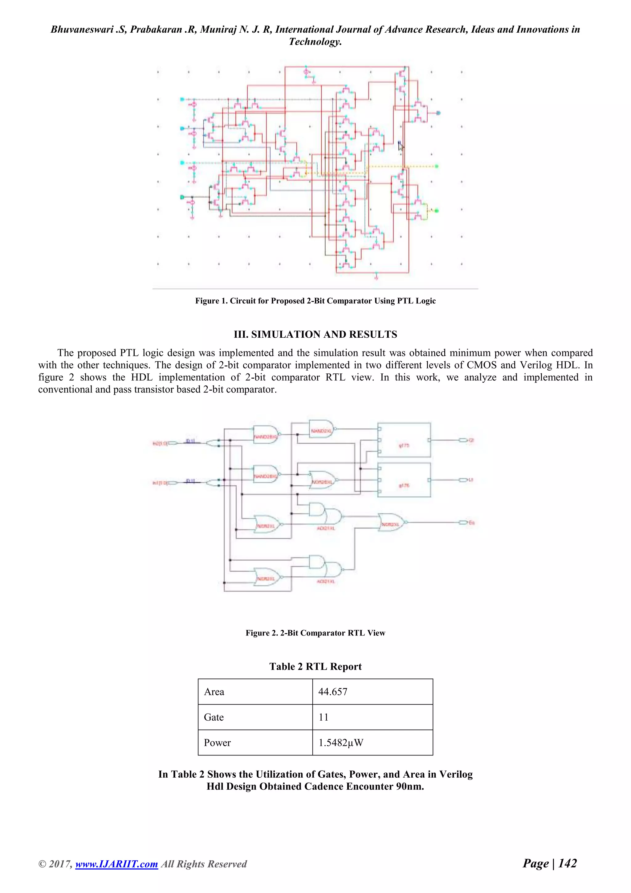
![Bhuvaneswari .S, Prabakaran .R, Muniraj N. J. R, International Journal of Advance Research, Ideas and Innovations in Technology. © 2017, www.IJARIIT.com All Rights Reserved Page | 141 By enhancing the performance of the XOR gate, the performance of the full adder can be improved [7]. The XOR and XNOR gates are the basic building blocks of a full adder circuit. XNOR / XOR design with less number of transistors, lesser power dissipation, and delay. XOR operation can be obtained with the addition of additional inverter. XNOR gate with three transistors has been less power dissipation [8]. The pass transistor logic style is used to reduce the transistor count and power dissipation using full adder circuit [9]. Different adder logic styles have been designed using 1 CMOS adder, but novel full adder designed using hybrid-CMOS design style is presented in that paper targets low PDP. But average power delay product will be occurred [10]. A CMOS full adder design using pass transistor logic as to low-power high-speed adder has become one of the most important and essential researches [11]. Pass transistor logic describes several logic families in an integrated circuit. It reduces the count of transistors used to make different logic gates by eliminating redundant transistors. PTL logic is used to reduce both transistor count and power dissipation in magnitude comparator is used to improve the good quality performance of this circuit. The circuit design of 2-bit comparator has been implemented in Cadence virtuoso TMSC 180nm CMOS technology and then it’s to generate the layout design. II. PROPOSED SYSTEM The implementation of 2 bit comparator is designed which provide the three output. Whether the first number is less than, equal to or greater than the third number. These are designed from basic logic gates are AND, NOR and NOT which compare the binary signals present at their input terminals and gives the output based on the signals applied to the input terminal. This 2-bits comparator which is designed by using the PTL approach to obtain the better performance interns of reducing the number of the transistor so the power also consumes very low. The pass transistor is driven by a periodic clock signal and acts as an access switch to either charge up or charge down the parasitic capacitance Cx, depending on the input signal Vin. If implemented from simple gates, it requires more transistors than any other function. In conventional logic families input is applied to gate terminal of the transistor but in PTL it is also applied to source and terminal. These circuit act as switch use either NMOS transistor or a parallel pair of NMOS and PMOS transistor. The width of PMOS of taken equal to NMOS. So that both transistors can pass the signal simultaneously in parallel. It reduces the count of transistors used to make different logic gates, by eliminating redundant transistors. Transistors are used as switches to pass logic levels between nodes of a circuit, instead of as switches connected directly to supply voltages. In this design style, the transistor acts as a switch to pass logic levels from input to output. Schematic of 2-bit magnitude comparator using pass transistor logic style is given in Figure1. Table 1 Simulation Result for 2 Bit Comparator S. No Circuit Logic Power Consumption (µW) 1. 2-bit comparator in digital 1.548 2. 2-bit comparator in CADENCE 3.658 3. Conventional 2-bit comparator 3.41 4. 2-bit comparator PTL logic 1.394](https://image.slidesharecdn.com/efficientimplementationof2-bitmagnitudecomparatorusingpt-180109055318/75/Efficient-implementation-of-2-bit-magnitude-comparator-using-pt-2-2048.jpg)
![Bhuvaneswari .S, Prabakaran .R, Muniraj N. J. R, International Journal of Advance Research, Ideas and Innovations in Technology. © 2017, www.IJARIIT.com All Rights Reserved Page | 143 Figure 3. Output of Proposed 2-Bit Comparator Using PTL Logic Figure 4. Graphical Representation Of 2-bit Comparator The pass transistor logic was optimizing the number of the transistor of the 2-bit comparator when compare with the traditional one and also it may possible to reduce the power dissipation. Here the 2-bit comparator using PTL logic power output is shown in Figure 3. The comparator was designed and implemented in CMOS 180nm technology and the result was obtained in each technique is shown in table 1 and the graphical representation of performance shown in figure 4. CONCLUSION The 2-bit magnitude comparator is designed which provide the three output. Whether the first number is less than, equal to or greater than the third number. This 2-bit comparator which is designed by the approach of PTL provides good performance by reducing transistor count as well as power because PTL logic helps in reducing the transistor count and it gives good result in terms of power consumption also maintain the low complexity of the circuit. Analyzing the simulation results of the proposed design to obtaining the minimum total power dissipation 1.394µW. The final results obtained in terms of transistor count and power of the device shows that PTL logic helps in reducing the transistor count. This improves the circuit performance. So it depends on the designer and it is a requirement which logic style is to be used and can be helpful in the implementation of higher design application such as Digital Signal Processors (DSP) and Data Processing etc., all the results are simulated using CMOS technology. REFERENCES [1] Suman Deb and S. Chaudhary, “High-Speed Comparator Architectures for Fast Binary Comparison”, IEEE International Conference on Emerging Applications of Information Technology, pp. 454-457, 2012. [2] Anjuli and Satyajit Anand, “2-Bit Magnitude Comparator design using different logic styles,” International Journal of Engineering Science Invention, Vol. 2, No. 1, pp.13-24, 2013. [3] Anjali Sharma, Richa Singh, Rajesh Mehra, Member, IEEE, “Low Power TG Full Adder Design Using CMOS Nano Technology,” IEEE International Conference on Parallel, Distributed and Grid Computing, pp. 210-213. [4] Vijay Kumar Sharma, Manisha Pattanaik, “VLSI Scaling methods and Low Power CMOS Buffer Circuit”, International Journal of Semiconductors, Vol. 34, No. 9, pp. 1-8, 2013. [5] Dinesh Sharma and Rajesh Mehra, “Low power Delay Optimized Buffer Design using 70nm CMOS Technology,” International Journal of Computer Applications, Vol.22, No. 3, pp.13-18, 2011.](https://image.slidesharecdn.com/efficientimplementationof2-bitmagnitudecomparatorusingpt-180109055318/75/Efficient-implementation-of-2-bit-magnitude-comparator-using-pt-4-2048.jpg)
![Bhuvaneswari .S, Prabakaran .R, Muniraj N. J. R, International Journal of Advance Research, Ideas and Innovations in Technology. © 2017, www.IJARIIT.com All Rights Reserved Page | 144 [6] P. Saini and R. Mehra, “A Novel Technique for Glitch and Leakage Power Reduction in CMOS VLSI Circuits,” International Journal of Advanced Computer Science and Application, Vol.3, No.10, pp.161-168, 2012. [7] Vandana Choudhary and Rajesh Mehra, “2-bit Comparator using Different Logic Style of Full Adder,” International Journal of Soft Computing and Engineering, Vol. 3, No.2, pp.277-279, 2013. [8] Manoj Kumar, Sandeep K. Arya1, and Sujata Pandey, “ Single bit full adder design using 8 transistors with novel 3 transistors XNOR gate”, International Journal of VLSI design & Communication Systems, Vol. 2, No. 4, pp. 47-59,2011. [9] Meena Aggarwal, Rajesh Mehra, “ Hybridized Power Efficient 32-bit Comparator using Less Transistor count”, International Journal of Advanced Research in Electronics and Communication Engineering, Vol. 4, No. 7, pp. 2012-2018, 2015. [10] Subodh Wairya, Himanshu Pandey, Rajendra Kumar Nagaria, Sudarshan Tiwari, “Ultra Low Voltage High Speed 1-bit CMOS Adder,” International Conference on Power Control And Embedded System, Vol.3, No.2, pp. 221-242, 2010. [11] Chiou-Kou Tung, Yu-Cherng Hung, Shao-Hui Shieh, Guo- Shing Huang, “A Low -Power High-speed Hybrid CMOS Full Adder For Embedded System,” IEEE Transaction on Design and Diagnostics of Electronic Circuits and Systems, Vol.13, No.6, pp.1- 4, 2007. Authors S. Bhuvaneswari is presently pursuing a master degree in VLSI design at Tejaa Shakthi institute of technology for women, Coimbatore. She is interested in CMOS VLSI design using cadence virtuoso. Prabakaran .R presently doing part time Ph.D. in Anna University, Chennai and worked as a research associate in Department of ECE at Tejaa Shakthi Institute Of Technology, Coimbatore. He has more than 3 year’s research experience in the field of VLSI Design. His research area includes CMOS and RF IC design, VLSI signals processing, Neural Networks, and MEMS.](https://image.slidesharecdn.com/efficientimplementationof2-bitmagnitudecomparatorusingpt-180109055318/75/Efficient-implementation-of-2-bit-magnitude-comparator-using-pt-5-2048.jpg)

This document presents the design and implementation of a 2-bit magnitude comparator using pass transistor logic (PTL) to minimize power consumption and transistor count. The comparator was designed in Cadence Virtuoso using 180nm CMOS technology, achieving a total power dissipation of 1.394μW. The proposed design demonstrates improved efficiency in logic operations relevant to applications such as digital signal processors and data processing systems.