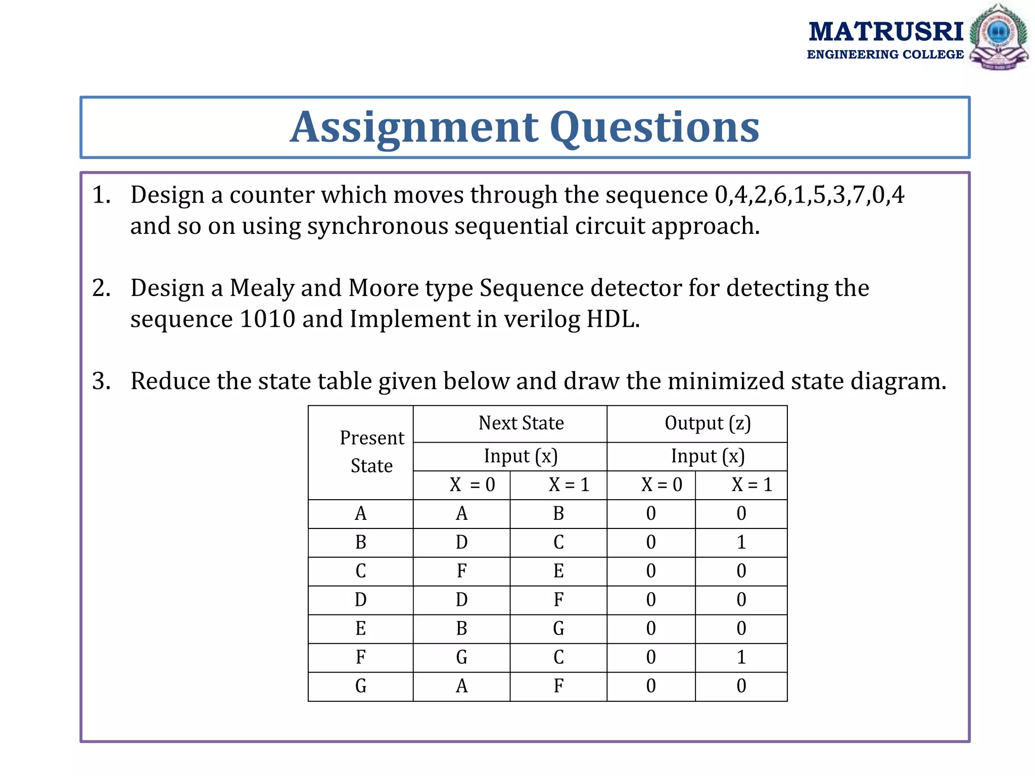
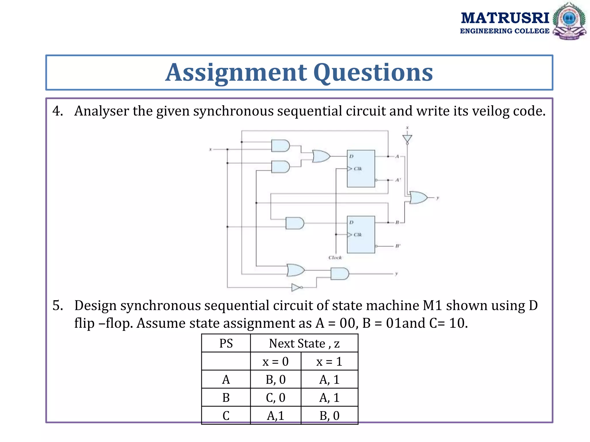
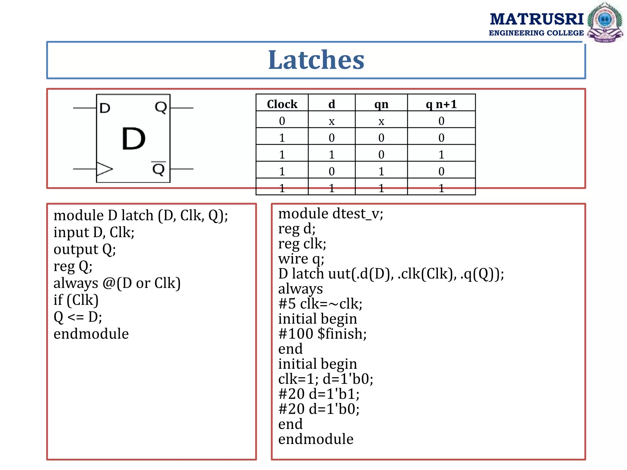
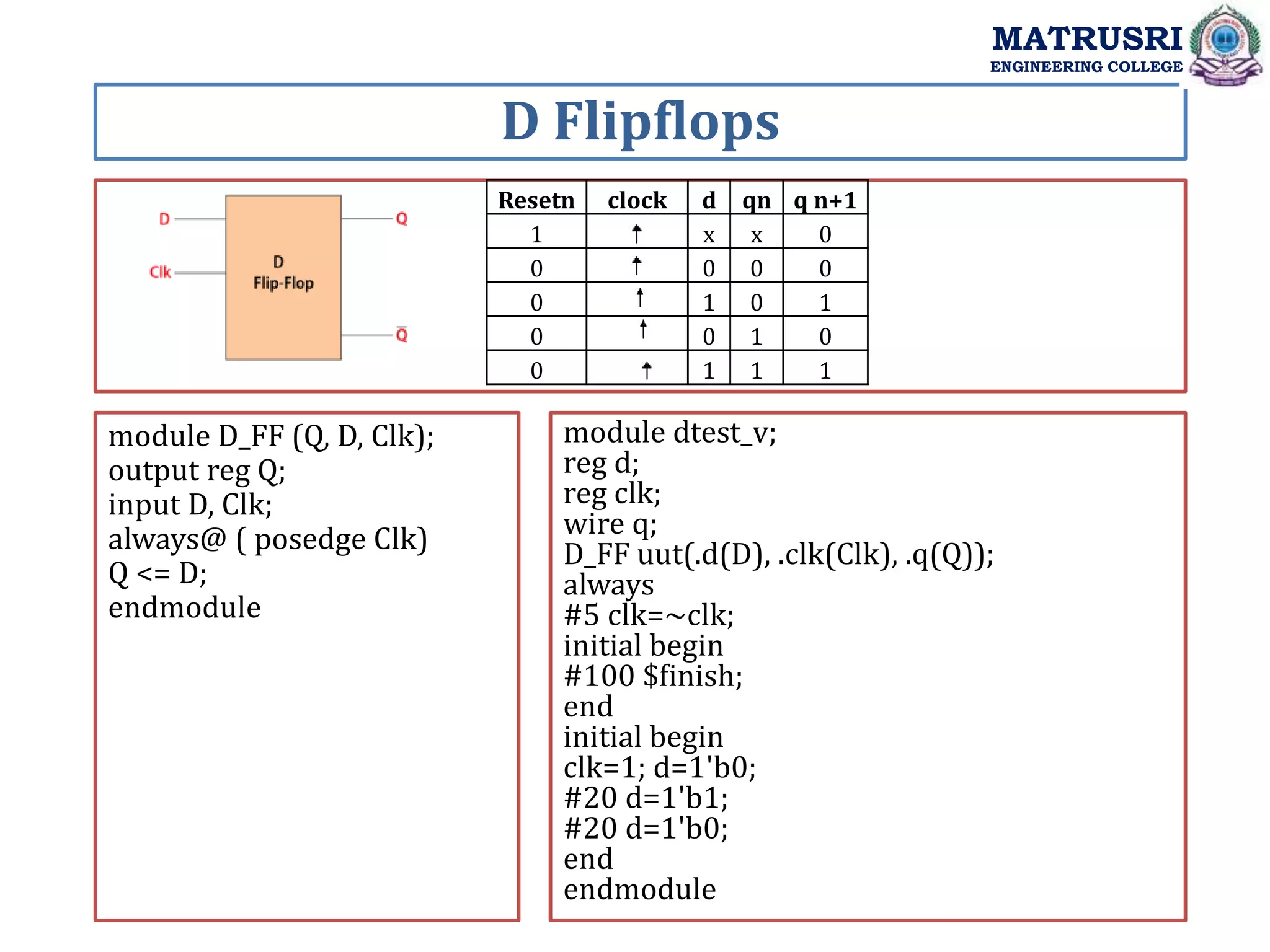
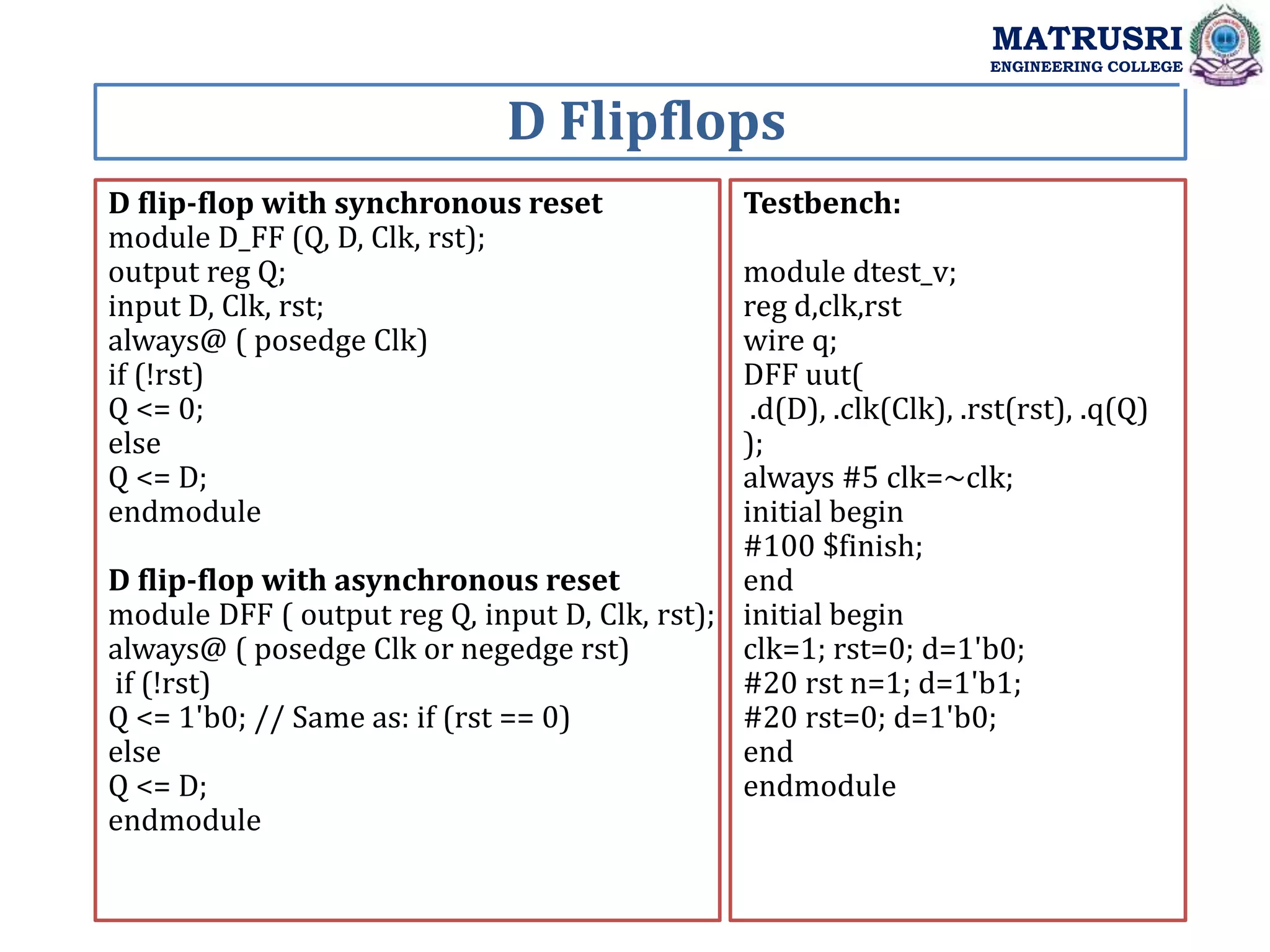
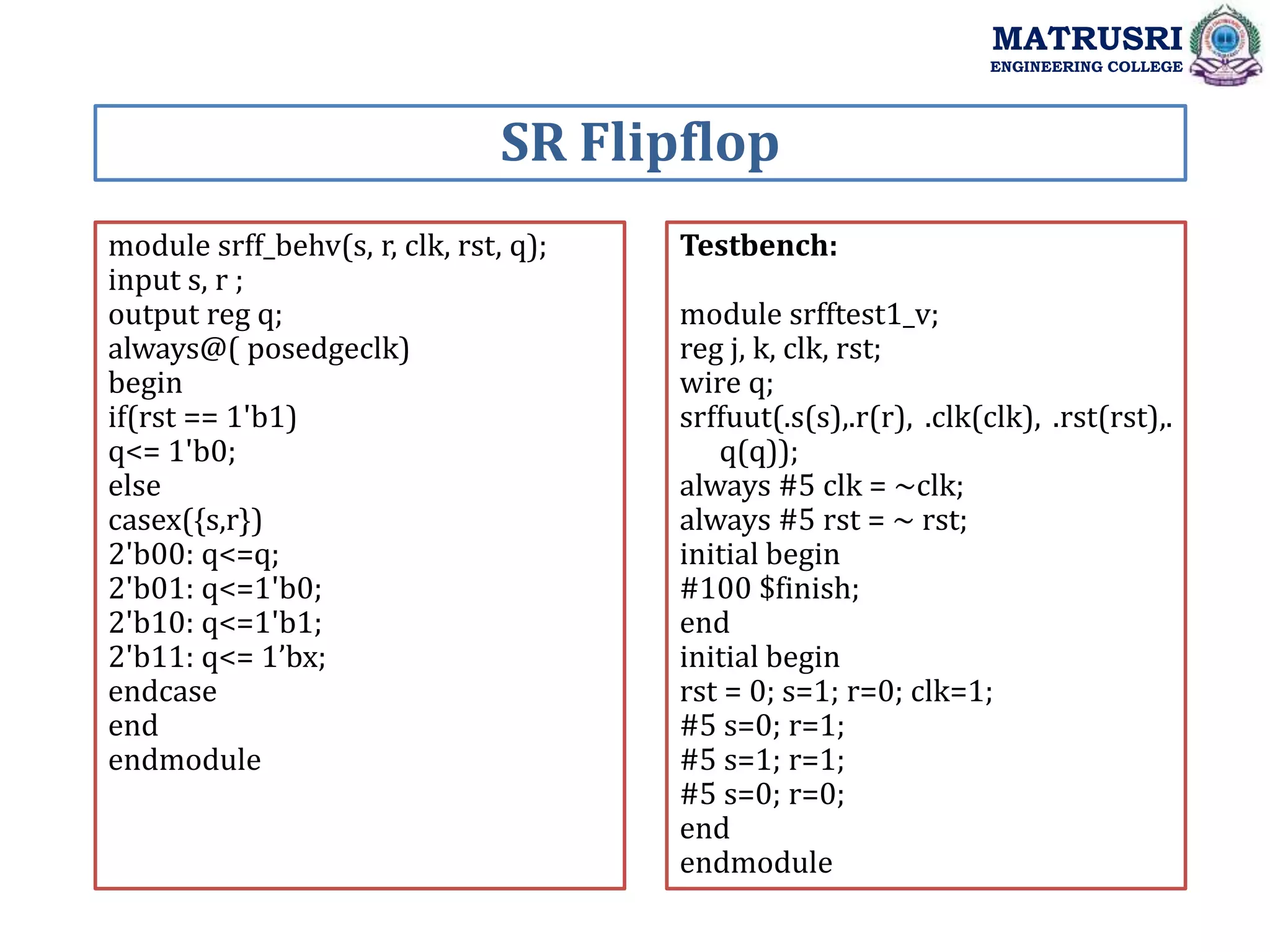
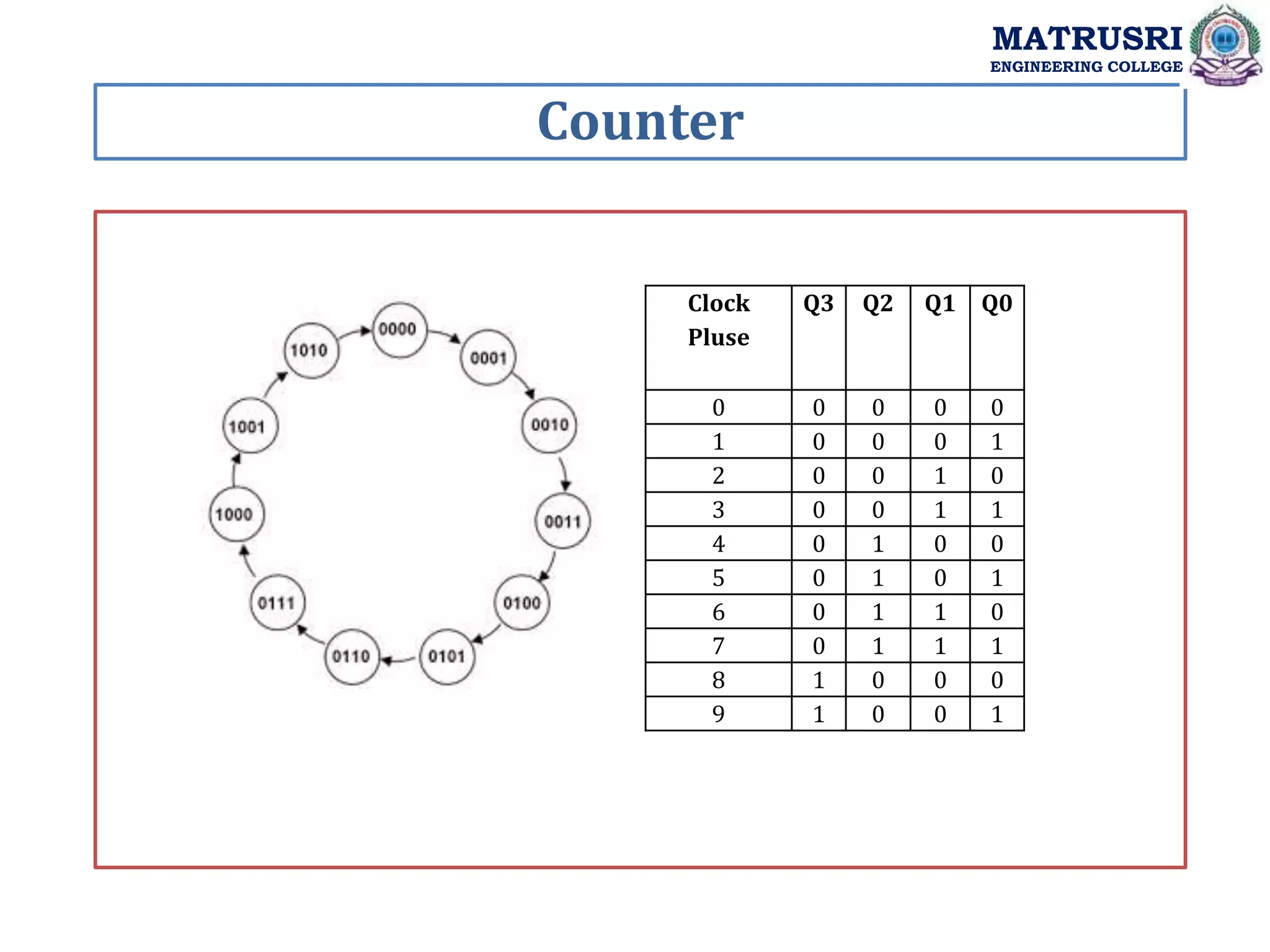
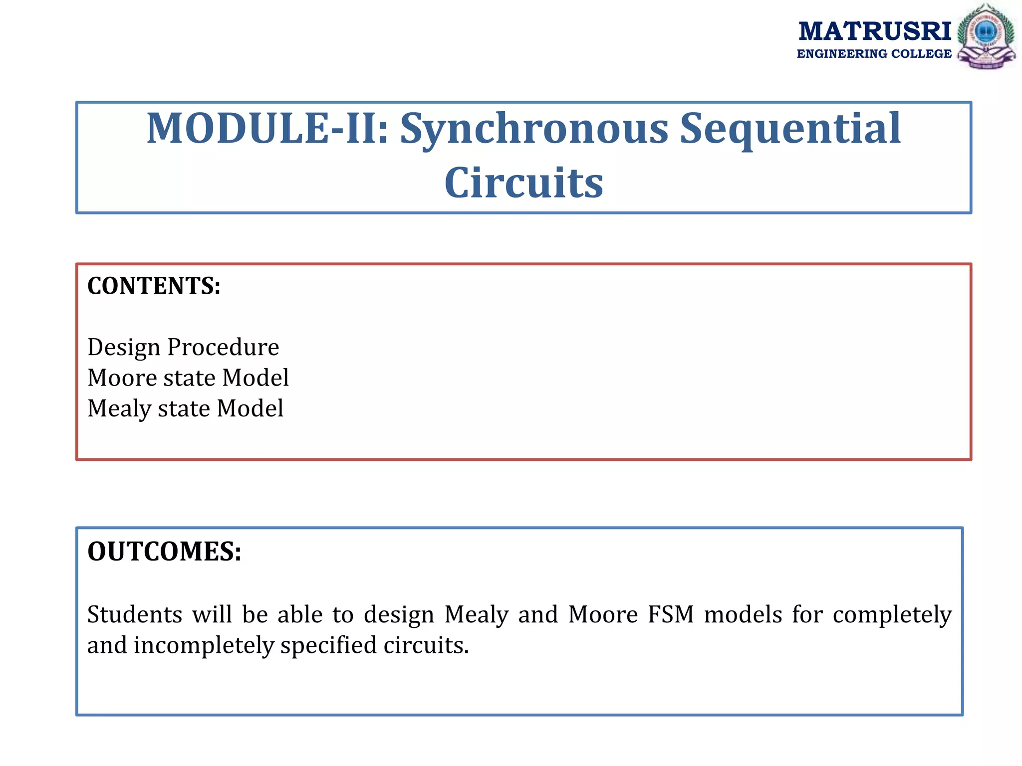
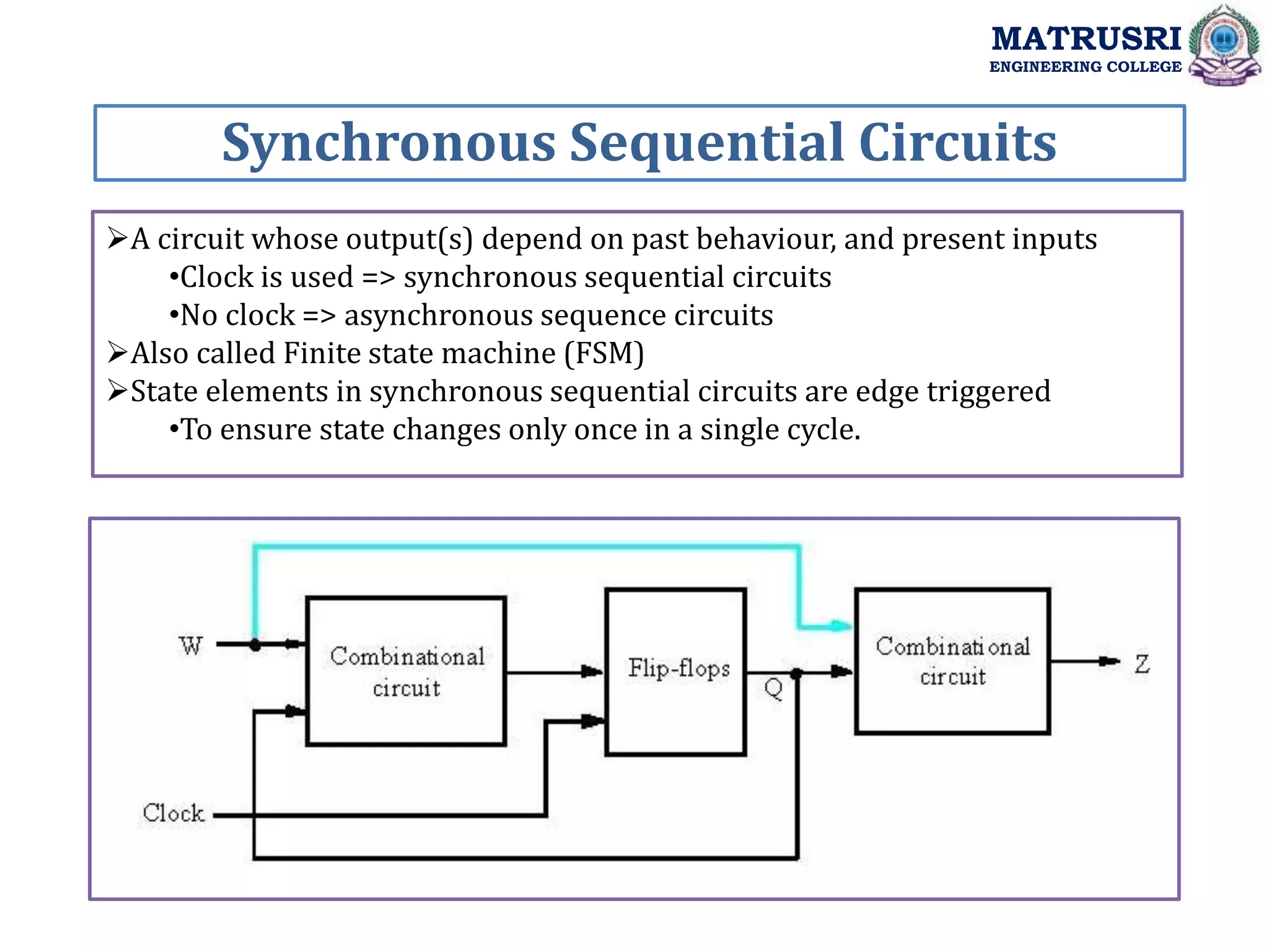
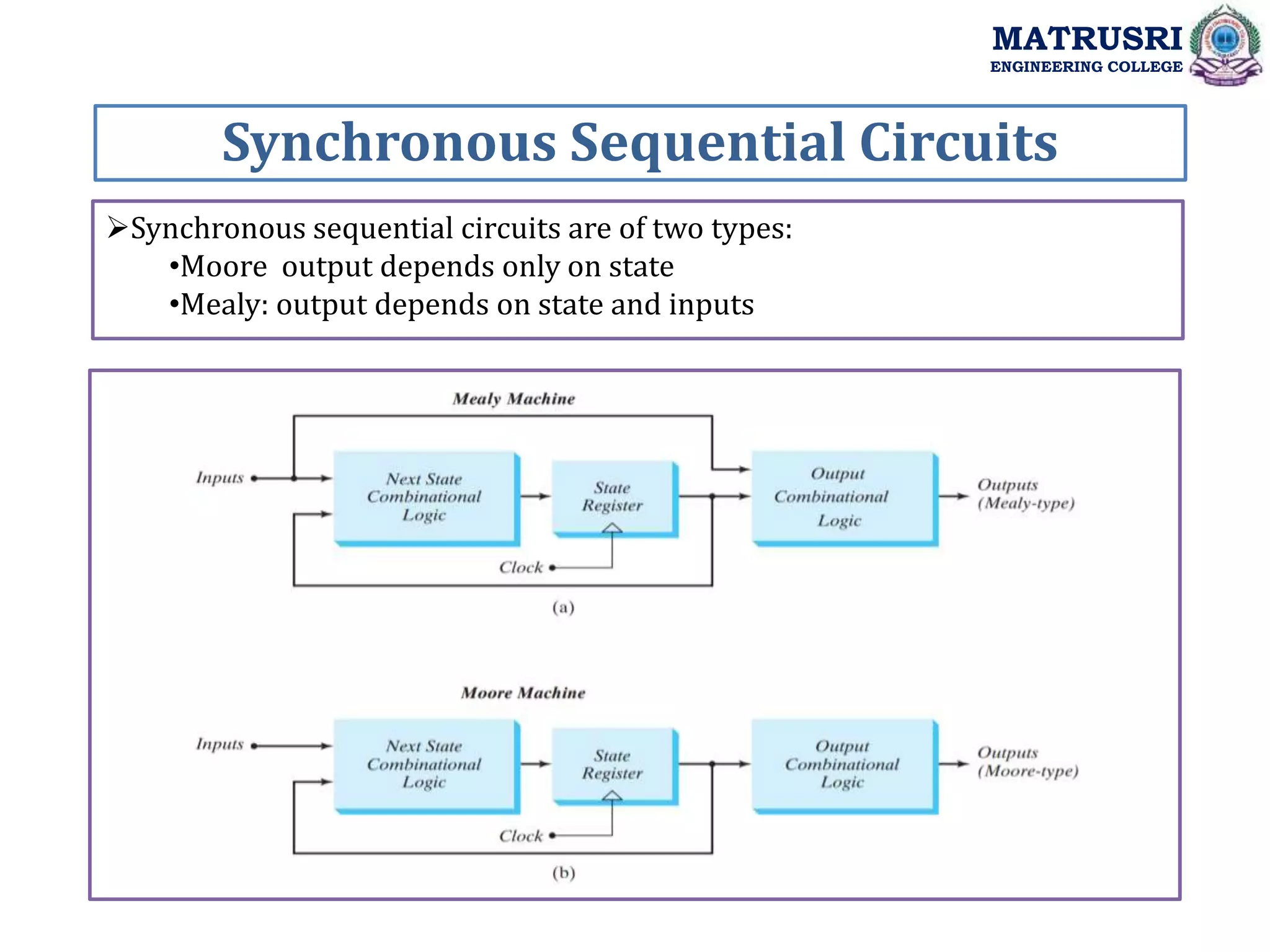
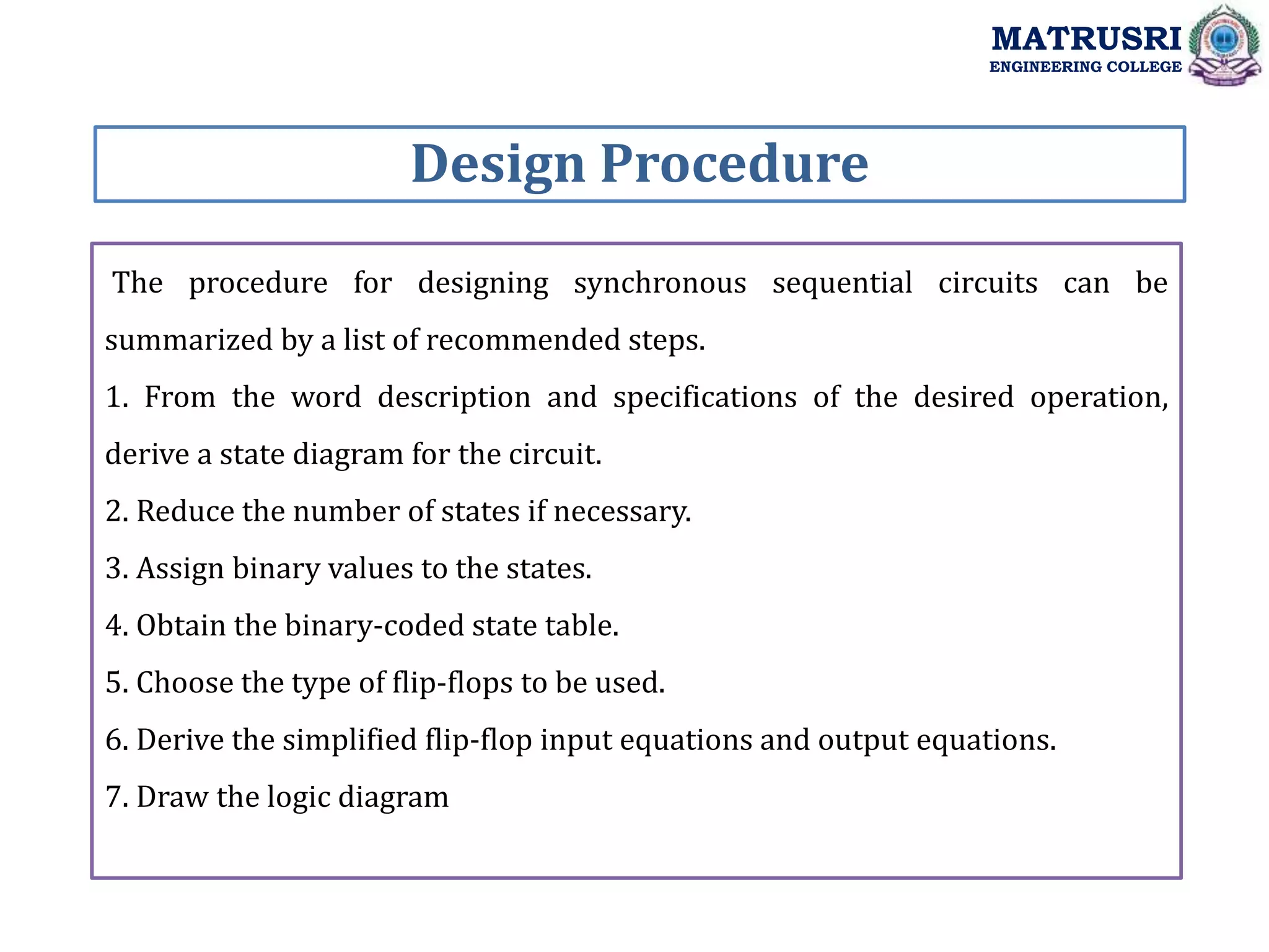
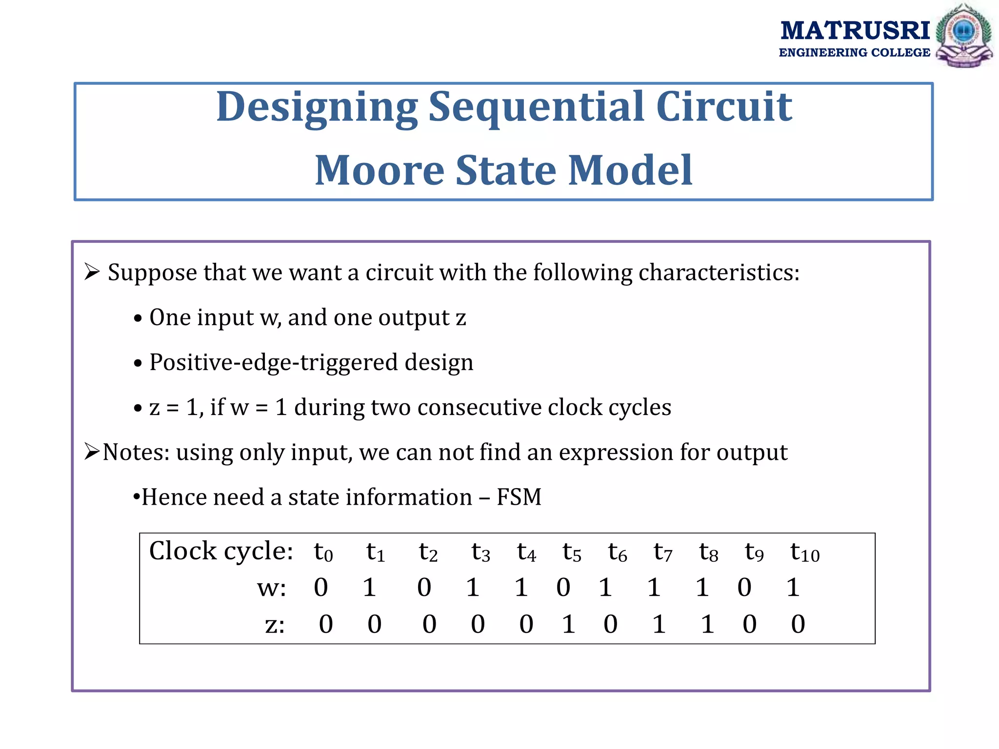
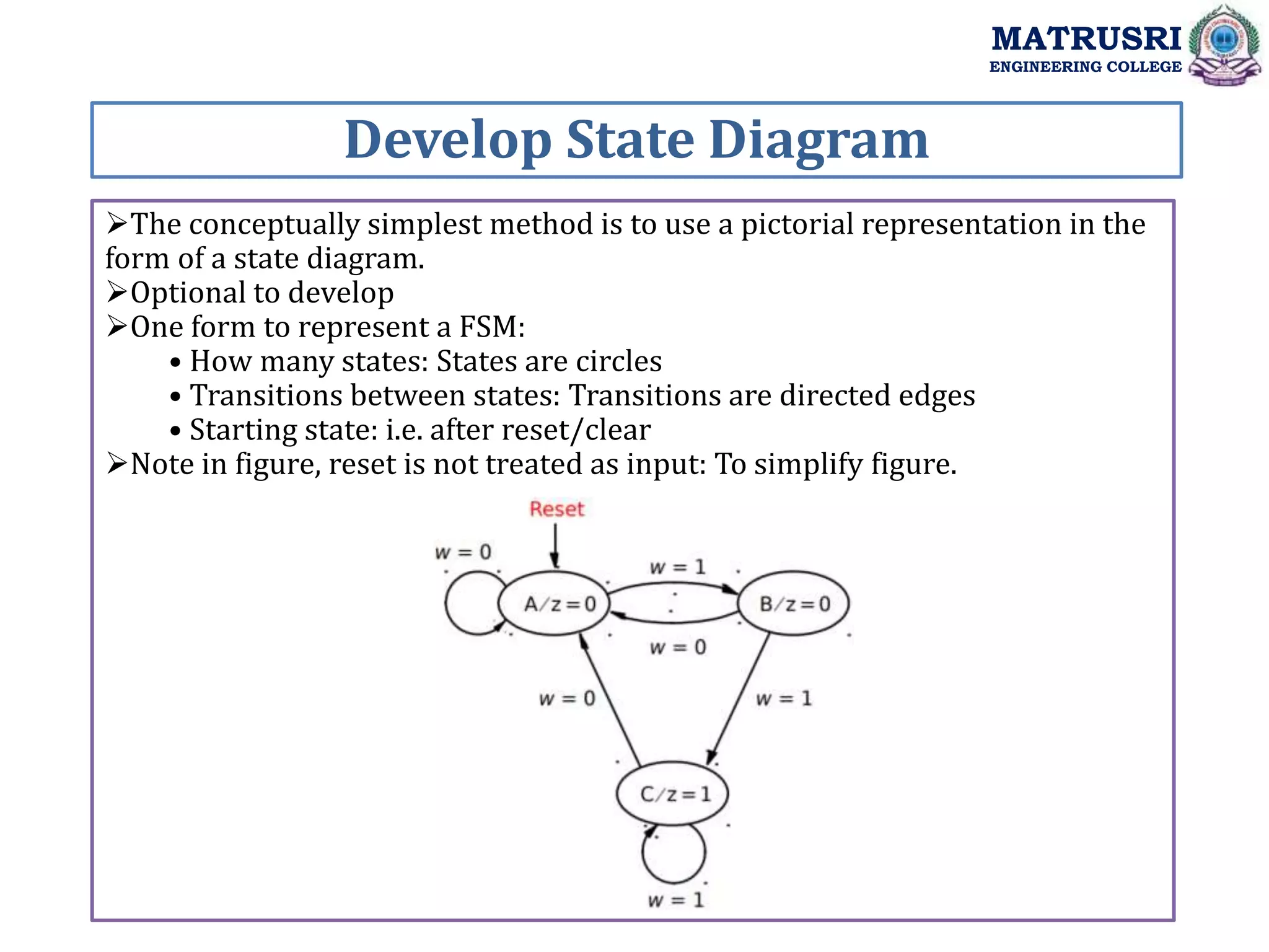
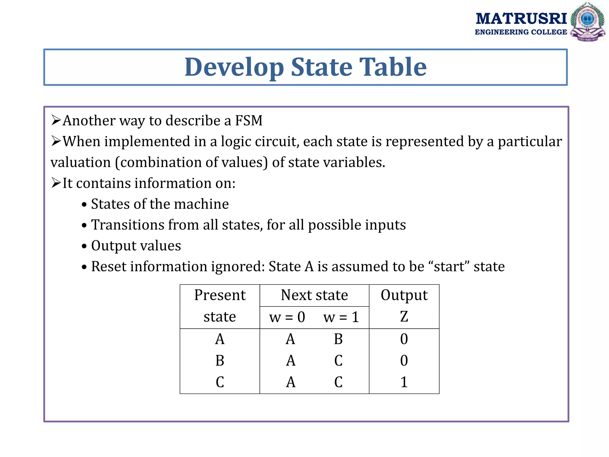
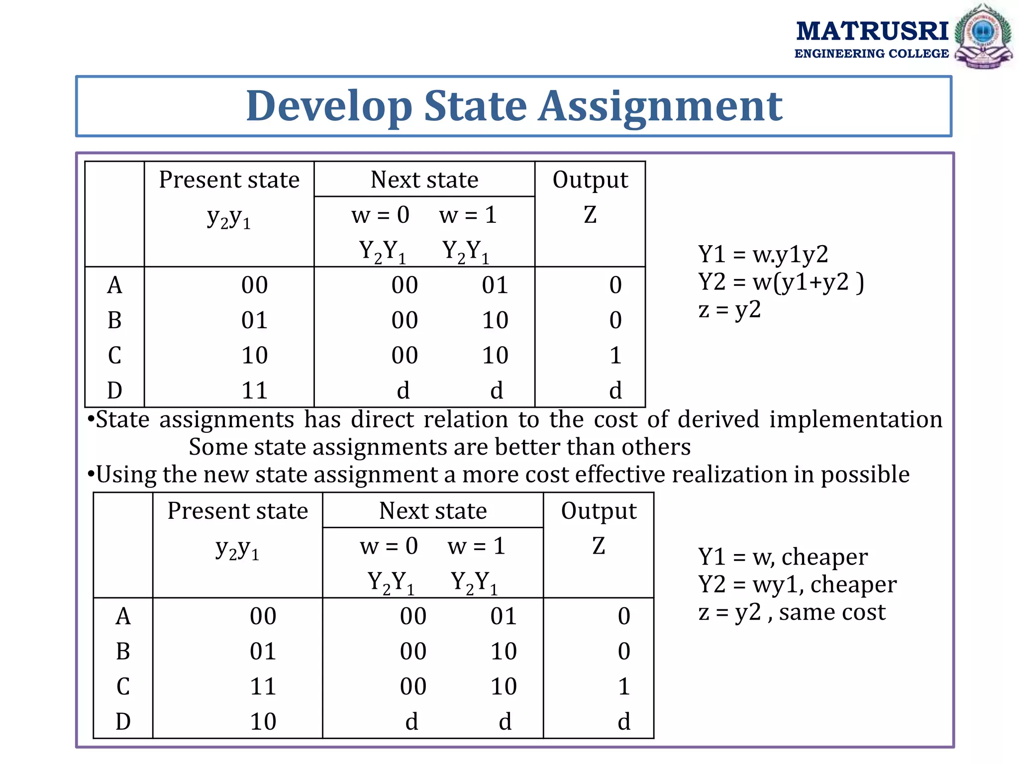
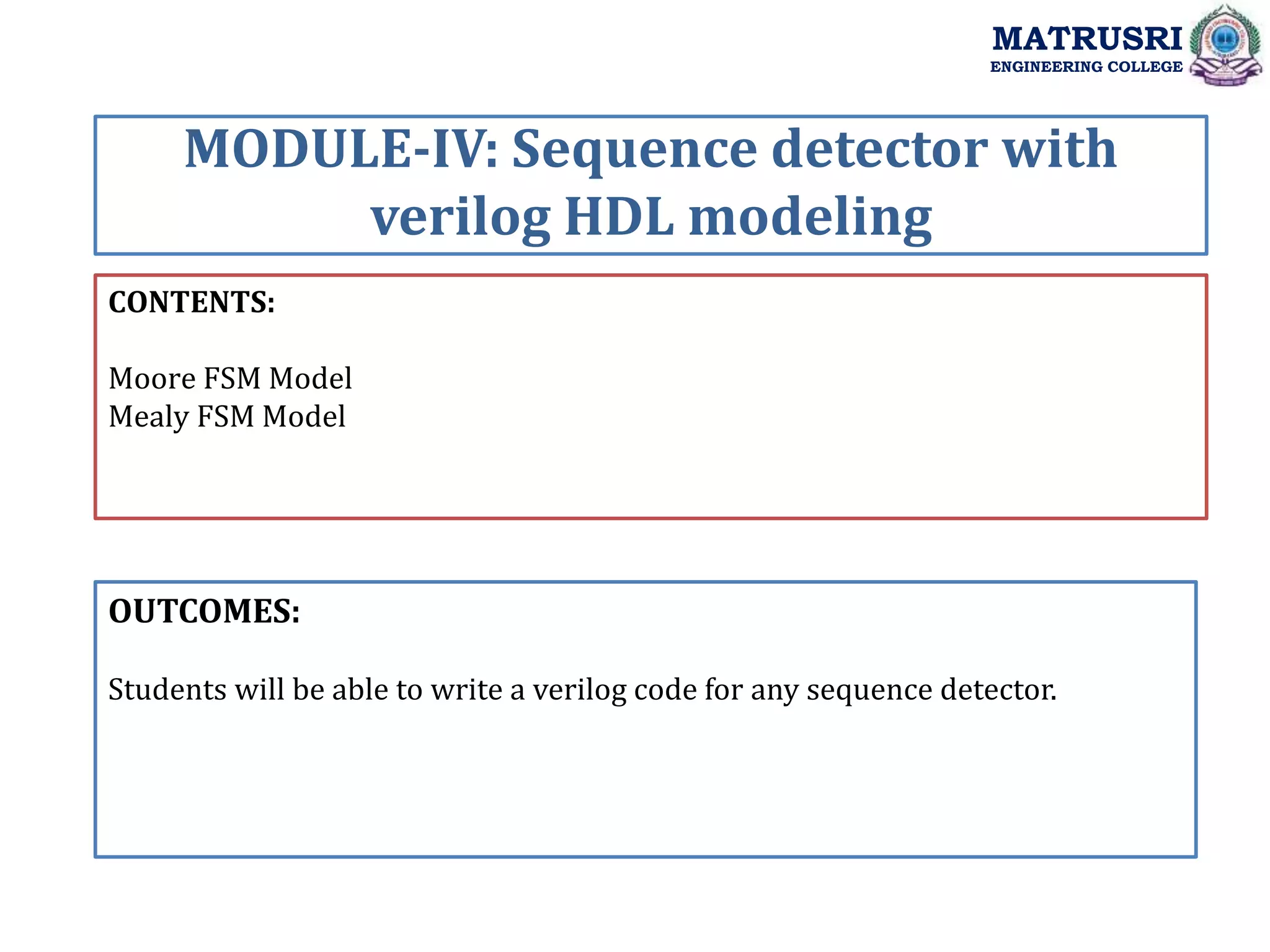
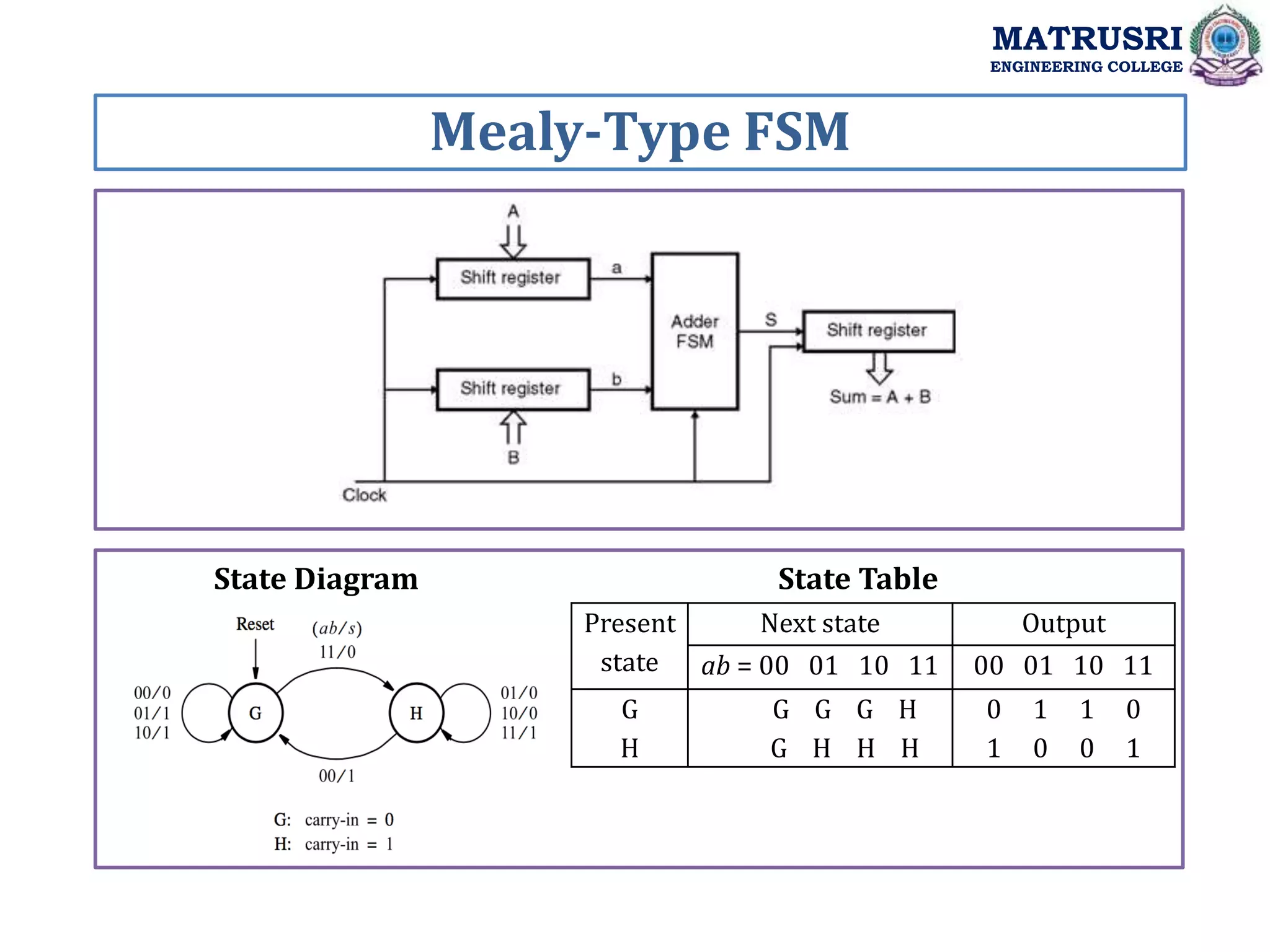
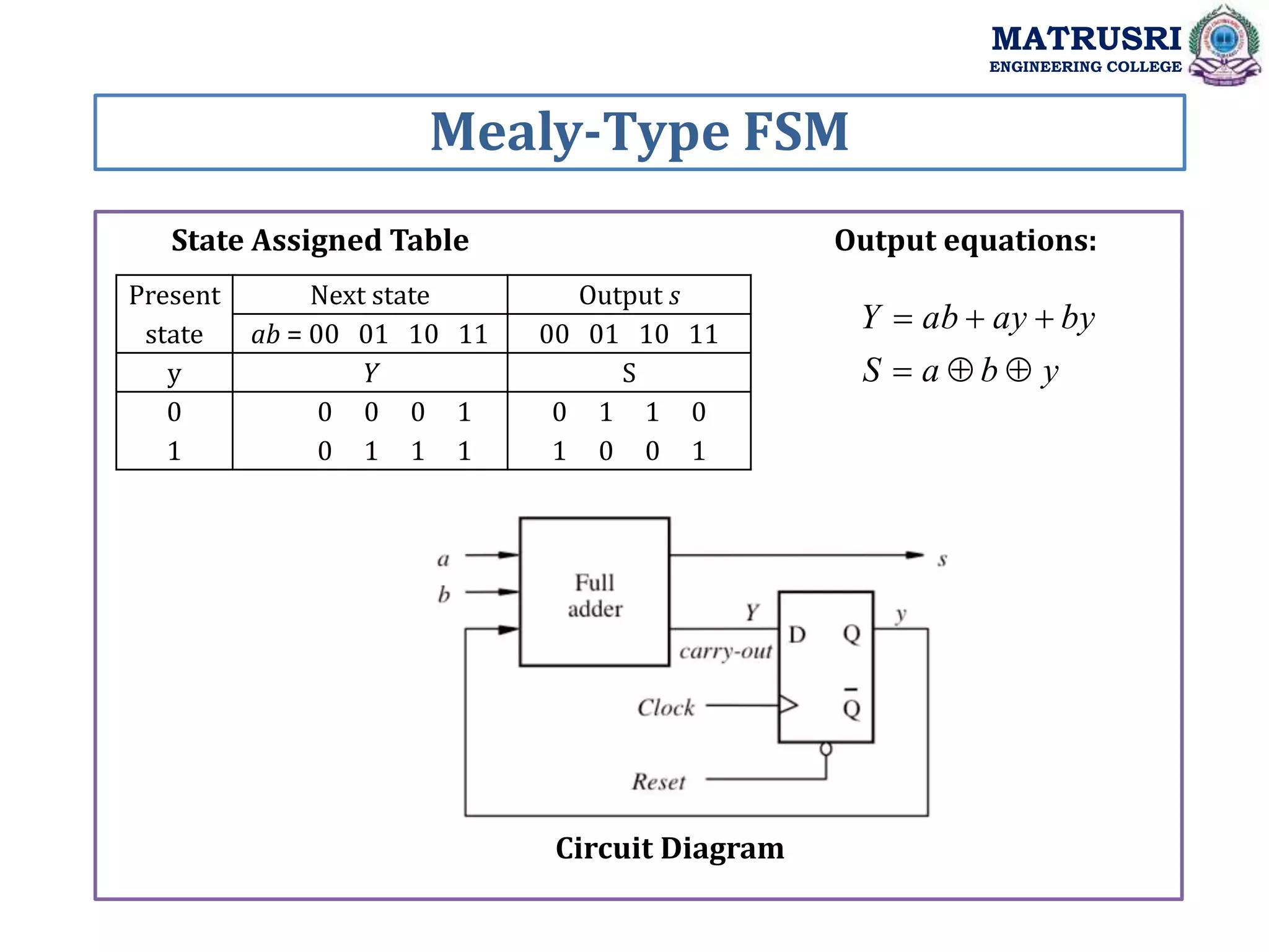
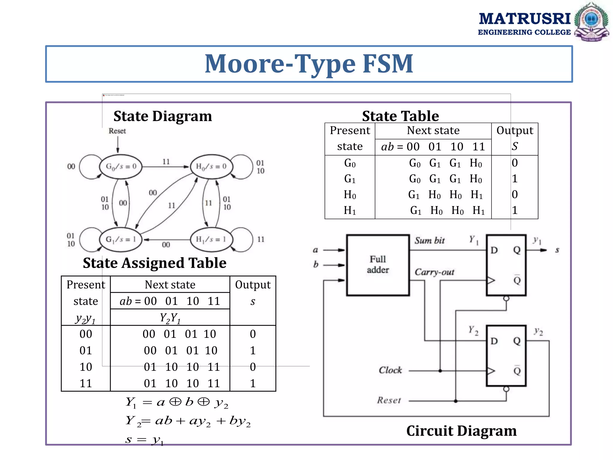
MATRUSRI ENGINEERING COLLEGE DEPARTMENT OF ELECTRONICS AND COMMUNICATION ENGINEERING SUBJECT NAME: DIGITAL SYSTEM DESIGN WITH VERILOG FACULTY NAME: Mrs. B. Indira Priyadarshini MATRUSRI ENGINEERING COLLEGE
INTRODUCTION: Gives a detailed presentation of synchronous sequential circuits (finite state machines). It explains the behavior of these circuits and develops practical design techniques for both manual and automated design.Deals with a general class of circuits in which the outputs depend on the past behavior of the circuit, as well as on the present values of inputs. They are called sequential circuits. In most cases a clock signal is used to control the operation of a sequential circuit; such a circuit is called a synchronous sequential circuit. UNIT-III OUTCOMES: After successful completion of this Unit students should be able to Analyze, design and implement sequential logic circuits in terms of state machines. Implement sequential circuits using Verilog code MATRUSRI ENGINEERING COLLEGE
CONTENTS: Latches Flip Flops Counters Shift registers applications OUTCOMES: Students will be able to design sequential logic modules in behavioral modeling. MODULE-I: Behavioural modeling of sequential logic modules MATRUSRI ENGINEERING COLLEGE
Latches MATRUSRI ENGINEERING COLLEGE Clock d qn q n+1 0 x x 0 1 0 0 0 1 1 0 1 1 0 1 0 1 1 1 1 module D latch (D, Clk, Q); input D, Clk; output Q; reg Q; always @(D or Clk) if (Clk) Q <= D; endmodule module dtest_v; reg d; reg clk; wire q; D latch uut(.d(D), .clk(Clk), .q(Q)); always #5 clk=~clk; initial begin #100 $finish; end initial begin clk=1; d=1'b0; #20 d=1'b1; #20 d=1'b0; end endmodule
D Flipflops MATRUSRI ENGINEERING COLLEGE module D_FF (Q, D, Clk); output reg Q; input D, Clk; always@ ( posedge Clk) Q <= D; endmodule module dtest_v; reg d; reg clk; wire q; D_FF uut(.d(D), .clk(Clk), .q(Q)); always #5 clk=~clk; initial begin #100 $finish; end initial begin clk=1; d=1'b0; #20 d=1'b1; #20 d=1'b0; end endmodule Resetn clock d qn q n+1 1 x x 0 0 0 0 0 0 1 0 1 0 0 1 0 0 1 1 1
D Flipflops MATRUSRI ENGINEERING COLLEGE D flip-flop with synchronous reset module D_FF (Q, D, Clk, rst); output reg Q; input D, Clk, rst; always@ ( posedge Clk) if (!rst) Q <= 0; else Q <= D; endmodule D flip-flop with asynchronous reset module DFF ( output reg Q, input D, Clk, rst); always@ ( posedge Clk or negedge rst) if (!rst) Q <= 1'b0; // Same as: if (rst == 0) else Q <= D; endmodule Testbench: module dtest_v; reg d,clk,rst wire q; DFF uut( .d(D), .clk(Clk), .rst(rst), .q(Q) ); always #5 clk=~clk; initial begin #100 $finish; end initial begin clk=1; rst=0; d=1'b0; #20 rst n=1; d=1'b1; #20 rst=0; d=1'b0; end endmodule
T Flipflops MATRUSRI ENGINEERING COLLEGE T Flipflop module tff_behv(t, clk, rst, q); input t, clk, rst; output reg q; always@(posedge clk) if(rst == 1) q<=1'b0; else begin if(t==1) q<= ~q; else q<= q; end endmodule Testbench: module tfftest_v; reg t, clk,rst; wire q; tffuut( .t(t), .clk(clk), .rst(rst), .q (q)); always #5 clk = ~clk; initial begin #100 $finish; end initial begin clk= 1; rst = 1; t=0; #5 t=0; #10 rst=0; t=1; #30 t=0; end endmodule Resetn clock t qn q n+1 1 x x 0 0 0 0 0 0 1 0 1 0 0 1 1 0 1 1 0
JK Flipflop MATRUSRI ENGINEERING COLLEGE
JK Flipflop MATRUSRI ENGINEERING COLLEGE module jkff_behv(j, k, clk, rst, q,qb); input j, k, clk, rst; output reg q; output qb; assign qb=~q; always@( posedge clk) begin if(rst == 1'b1) q<= 1'b0; else case({j,k}) 2'b00: q<=q; 2'b01: q<=1'b0; 2'b10: q<=1'b1; 2'b11: q<= ~q; endcase end endmodule Testbench: module jkfftest1_v; reg j, k, clk, rst; wire q, qb; jkffuut(.j(j),.k(k), .clk(clk), .rst(rst),. q(q),.qb(qb)); always #5 clk = ~clk; always #5 rst = ~ rst; initial begin #100 $finish; end initial begin rst = 0; j=1; k=0; clk=1; #5 j=0; k=1; #5 j=1; k=1; #5 j=1; k=0; end endmodule
SR Flipflop MATRUSRI ENGINEERING COLLEGE rst clk s r qn q n+1 1 x x x 0 0 0 0 0 0 0 0 0 1 1 0 0 1 0 0 0 0 1 1 0 0 1 0 0 1 0 1 0 1 1 0 1 1 x x 0 1 1 x x
SR Flipflop MATRUSRI ENGINEERING COLLEGE module srff_behv(s, r, clk, rst, q); input s, r ; output reg q; always@( posedgeclk) begin if(rst == 1'b1) q<= 1'b0; else casex({s,r}) 2'b00: q<=q; 2'b01: q<=1'b0; 2'b10: q<=1'b1; 2'b11: q<= 1’bx; endcase end endmodule Testbench: module srfftest1_v; reg j, k, clk, rst; wire q; srffuut(.s(s),.r(r), .clk(clk), .rst(rst),. q(q)); always #5 clk = ~clk; always #5 rst = ~ rst; initial begin #100 $finish; end initial begin rst = 0; s=1; r=0; clk=1; #5 s=0; r=1; #5 s=1; r=1; #5 s=0; r=0; end endmodule
Counter MATRUSRI ENGINEERING COLLEGE Clock Pluse Q3 Q2 Q1 Q0 0 0 0 0 0 1 0 0 0 1 2 0 0 1 0 3 0 0 1 1 4 0 1 0 0 5 0 1 0 1 6 0 1 1 0 7 0 1 1 1 8 1 0 0 0 9 1 0 0 1
Counter MATRUSRI ENGINEERING COLLEGE module updowncount ( R, clk, L, E, updwn, Q ); parameter n = 8; input [n-1]R; input clk, L, E, updwn; output [n-1] Q; reg [n-1]Q; integer direction; always @(posedge clk) begin if (updwn) direction = 1; else direction = −1; if (L) Q <= R; else if (E) Q <= Q + direction; end endmodule Testbench: module updowncounttest_v; reg clk, L, E, updwn; reg [n-1]R wire [n-1:0] Q; Updowncount uut(R, clk, L, E, updwn, Q); always #5 clk= ~clk; initial begin #400 $finish; end initial begin L=1;clk=1;updwn=0; R=8’o23;E=1; #10 L=0; #150 L=1; #20 L=0; updwn=1; end endmodule
Shift Register MATRUSRI ENGINEERING COLLEGE Right Shift: module shift4 (R, L, w, Clock, Q); input [3:0] R; input L, w, Clock; output reg [3:0] Q; always @(posedge Clock) if (L) Q <= R; else Q[3:0]={w, Q[3: 1]}; endmodule Left Shift: module shift4 (R, L, w, Clock, Q); input [3:0] R; input L, w, Clock; output reg[3:0] Q; always @(posedge Clock) if (L) Q <= R; else Q[3:0]={Q[2: 0],w}; endmodule Testbench: module shift4_tst_v; reg L,w,Clock; reg [3:0]R; wire [3:0]Q; shift4 uut(R, L, w, Clock, Q); initial begin R = 4’b1011; L = 1; w = 1; #20; L = 0; end always #5 Clock = ~ Clock; endmodule
Shift Register MATRUSRI ENGINEERING COLLEGE Serial In Serial Out: module shift (C, SI, SO); input C,SI; output SO; reg [7:0] tmp; always @(posedge C) begin tmp = tmp << 1; tmp[0] = SI; end assign SO = tmp[7]; endmodule Parallel In Parallel Out: module pipo(pin, clk, reset, pout); input [3:0] pin; input clk, reset; output reg [3:0] pout; always @ (posedgeclk or posedge reset) begin if (reset) pout <= 4'b0000; else pout <= pin; end endmodule
Shift Register MATRUSRI ENGINEERING COLLEGE Parallel In Serial Out: module Shiftregister_PISO( Clk, Parallel_In,load, Serial_Out); input Clk,load; input [3:0]Parallel_In; output reg Serial_Out; reg [3:0]tmp; always @(posedge Clk) begin if(load) tmp<=Parallel_In; else begin Serial_Out<=tmp[3]; tmp<={tmp[2:0],1'b0}; end end endmodule Serial In Parallel Out: module ShiftRegister_SIPO(Clk, SI, PO); input Clk,SI; output [7:0] PO; reg [7:0] tmp; always @(posedge Clk) begin tmp = {tmp[6:0], SI}; end assign PO = tmp; endmodule
1. The output of latches will remain in set/reset until the trigger pulse is given to change the state. 2. The purpose of the clock input to a flip-flop is to cause the output to assume a state dependent on the controlling inputs. 3. How much storage capacity does each stage in a shift register represent? Ans: One bit 4. Binary counter that counts reversely is called down counter. Questions & Answers MATRUSRI ENGINEERING COLLEGE
CONTENTS: Design Procedure Moore state Model Mealy state Model OUTCOMES: Students will be able to design Mealy and Moore FSM models for completely and incompletely specified circuits. MODULE-II: Synchronous Sequential Circuits MATRUSRI ENGINEERING COLLEGE
Synchronous Sequential Circuits MATRUSRI ENGINEERING COLLEGE A circuit whose output(s) depend on past behaviour, and present inputs •Clock is used => synchronous sequential circuits •No clock => asynchronous sequence circuits Also called Finite state machine (FSM) State elements in synchronous sequential circuits are edge triggered •To ensure state changes only once in a single cycle.
Synchronous Sequential Circuits MATRUSRI ENGINEERING COLLEGE Synchronous sequential circuits are of two types: •Moore output depends only on state •Mealy: output depends on state and inputs
Design Procedure MATRUSRI ENGINEERING COLLEGE The procedure for designing synchronous sequential circuits can be summarized by a list of recommended steps. 1. From the word description and specifications of the desired operation, derive a state diagram for the circuit. 2. Reduce the number of states if necessary. 3. Assign binary values to the states. 4. Obtain the binary-coded state table. 5. Choose the type of flip-flops to be used. 6. Derive the simplified flip-flop input equations and output equations. 7. Draw the logic diagram
Designing Sequential Circuit Moore State Model MATRUSRI ENGINEERING COLLEGE  Suppose that we want a circuit with the following characteristics: • One input w, and one output z • Positive-edge-triggered design • z = 1, if w = 1 during two consecutive clock cycles Notes: using only input, we can not find an expression for output •Hence need a state information – FSM Clock cycle: t0 t1 t2 t3 t4 t5 t6 t7 t8 t9 t10 w: 0 1 0 1 1 0 1 1 1 0 1 z: 0 0 0 0 0 1 0 1 1 0 0
Develop State Diagram MATRUSRI ENGINEERING COLLEGE The conceptually simplest method is to use a pictorial representation in the form of a state diagram. Optional to develop One form to represent a FSM: • How many states: States are circles • Transitions between states: Transitions are directed edges • Starting state: i.e. after reset/clear Note in figure, reset is not treated as input: To simplify figure.
Develop State Table MATRUSRI ENGINEERING COLLEGE Another way to describe a FSM When implemented in a logic circuit, each state is represented by a particular valuation (combination of values) of state variables. It contains information on: • States of the machine • Transitions from all states, for all possible inputs • Output values • Reset information ignored: State A is assumed to be “start” state Present state Next state Output Z w = 0 w = 1 A B C A B A C A C 0 0 1
Develop State Assignment MATRUSRI ENGINEERING COLLEGE Find number of flip/flops needed to represent state •No. of FFs = log2(no. of states) Assign each state a combination of values of state variables • “State assigned table” • All unused variable combination are normally used as don’t cares Below is the resulting table after state assignment Notice that: •Output depends on current state only - Moore type •2 state variables are sufficient to represent 3 states •Y1 & Y2 are next-state variables, y1&y2 are present-state variables Need to decide type of FF to use as state element Use D-FF since it is easiest D1 = Y1, and D2 = Y2 For every next state and output, derive their function from present state and input
Develop State Assignment MATRUSRI ENGINEERING COLLEGE Y1 = w.y1y2 Y2 = w(y1+y2 ) z = y2 •State assignments has direct relation to the cost of derived implementation Some state assignments are better than others •Using the new state assignment a more cost effective realization in possible Y1 = w, cheaper Y2 = wy1, cheaper z = y2 , same cost Present state y2y1 Next state Output Z w = 0 w = 1 Y2Y1 Y2Y1 A B C D 00 01 10 11 00 01 00 10 00 10 d d 0 0 1 d Present state y2y1 Next state Output Z w = 0 w = 1 Y2Y1 Y2Y1 A B C D 00 01 11 10 00 01 00 10 00 10 d d 0 0 1 d
Function Realization MATRUSRI ENGINEERING COLLEGE
Resulting Logic Circuit MATRUSRI ENGINEERING COLLEGE
Timing Diagram of Realization MATRUSRI ENGINEERING COLLEGE
Mealy Machine Implementation MATRUSRI ENGINEERING COLLEGE Output values are generated using state & present inputs State diagram State Table State Assigned Table Logic Diagram Y = D = w z = wy Clock cycle: t0 t1 t2 t3 t4 t5 t6 t7 t8 t9 t10 w: 0 1 0 1 1 0 1 1 1 0 1 z: 0 0 0 0 1 0 0 1 1 0 0 Present state Next state Output z w = 0 w = 1 w = 0 w = 1 A B A B A B 0 0 0 1 Present state Next state Output z w = 0 w = 1 w = 0 w = 1 y Y Y z z A B 0 1 0 1 0 1 0 0 0 1
Timing Diagram of Mealy Machine MATRUSRI ENGINEERING COLLEGE Mealy implementation is more cost effective than Moore implementation •However, circuit can be modified so that it behaves like a Moore machine Note how output change based on state and input
1. Moore machine produces an output over the change of transition states. 2. In mealy machine, the O/P depends upon present states and inputs. 3. The relationship that exists among the inputs, outputs, present states and next states can be specified by either the state table or the state diagram. 4. A state-transition table is a table showing what state a finite-state machine will move to, based on the current state and other inputs. Questions & Answers MATRUSRI ENGINEERING COLLEGE
CONTENTS: State Minimization Partitioning Minimization Procedure OUTCOMES: Students will be able to design a more complex FSM with fewer flips-flops. MODULE-III: State Minimization MATRUSRI ENGINEERING COLLEGE
State Minimization MATRUSRI ENGINEERING COLLEGE Two states Si and Sj are said to be equivalent if and only if for every possible input sequence, the same output sequence will be produced regardless of whether Si or Sj is the initial state. Lower no. of states => lower no. of FFs Solved using “partitioning minimization procedure” Partition: A set of states A partition consists of one or more blocks, where each block comprises a subset of states that may be equivalent, but the states in a given block are definitely not equivalent to the states in other blocks. States in a partition may be equivalent Not equivalent to states in other partitions
State Minimization MATRUSRI ENGINEERING COLLEGE •P1 = (ABCDEFG) Partition based on output z •P2 = (ABD)(CEFG), Partition based on 0- & 1-successor for block (ABD) & (CEFG) •P3 = (ABD)(CEG)(F), Partition based on 0- & 1-successor for block (ABD) & (CEG), •P4 = (AD)(B)(CEG)(F) Partition based on 0- & 1-successor for block (AD) & (CEG), => Final •Final Partitions: P5 = (AD)(B)(CEG)(F) 2 FFs are sufficient after state minimization instead of 3 Present state Next state Output z w = 0 w = 1 A B C D E F G B C D F F E B G F C E D F G 1 1 0 1 0 0 0 Present state Next state Output z w = 0 w = 1 A B C F B C A F F C C A 1 1 0 0
Incompletely Specified FSMs MATRUSRI ENGINEERING COLLEGE The partitioning scheme for minimization of states works well when all entries in the state table are specified. FSMs of this type are said to be completely specified. If one or more entries in the state table are not specified, corresponding to don’t-care conditions, then the FSM is said to be incompletely specified. Affects the number of minimized states Assume x’s are zeros: P1 = (ABCDEFG) P2 = (ABDG)(CEF), P3 = (AB)(D)(G)(CE)(F), P4 = (A)(B)(D)(G)(CE)(F), P5 = P4 => 6 states Assume x’s are ones: P1 = (ABCDEFG) P2 = (AD)(BCEFG), P3 = (AD)(B)(CEFG), P4 = (AD)(B)(CEG)(F), P5 = P4 => 4 states Present state Next state Output z w = 0 w = 1 w = 0 w = 1 A B C D E F G B C D - F E B G F C E D F - 0 0 0 - 0 1 0 0 0 1 0 1 0 -
1. State Minimizing reduces the number of flips-flops used in the FSM. 2. State Minimizing reduces the complexity of the combinational circuit needed in the FSM. 3. By state minimization, two different FSMs may exhibit identical behavior in terms of the outputs produced in response to all possible inputs. 4. If one or more entries in the state table are not specified, corresponding to don’t-care conditions, then the FSM is said to be incompletely specified. Questions & Answers MATRUSRI ENGINEERING COLLEGE
CONTENTS: Moore FSM Model Mealy FSM Model OUTCOMES: Students will be able to write a verilog code for any sequence detector. MODULE-IV: Sequence detector with verilog HDL modeling MATRUSRI ENGINEERING COLLEGE
module simple (Clock, Resetn, w, z); input Clock, Resetn, w; output z; reg [2:1] y, Y; parameter [2:1] A = 2'b00, B = 2'b01, C = 2'b10; always @(w or y) case (y) A: if (w) Y = B; else Y = A; B: if (w) Y = C; else Y = A; C: if (w) Y = C; else Y = A; default: Y = 2'bxx; endcase always @(negedge Resetn or posedge Clock) if (Resetn == 0) y <= A; else y <= Y; assign z = (y == C); endmodule Moore FSM Model MATRUSRI ENGINEERING COLLEGE
MATRUSRI ENGINEERING COLLEGE module mealy (Clock, Resetn, w, z); input Clock, Resetn, w; output z; reg y, Y, z; parameter A = 0, B = 1; always @(w or y) case (y) A: if (w) begin z = 0; Y = B; end else begin z = 0; Y = A; end B: if (w) begin z = 1; Y = B; end else begin z = 0; Y = A; end endcase always @(negedge Resetn or posedge Clock) if (Resetn == 0) y <= A; else y <= Y; endmodule Mealy FSM Model
1. Mealy machine will have same or fewer states than Moore machine. 2. In Moore Machine both output and state change synchronous to the clock edge. 3. Moore Machine requires more hardware to design than mealy machine. 4. In Mealy machine, asynchronous output generation through the state changes synchronous to the clock. Questions & Answers MATRUSRI ENGINEERING COLLEGE
CONTENTS: Modulo – 8 Counter D Flip-flop JK Flip-flop Verilog code OUTCOMES: Students will be able to design different counters using sequential ciruit approach. MODULE-V: Modulo-8 Counter Using the Sequential Circuit Approach MATRUSRI ENGINEERING COLLEGE
Modulo-8 Counter MATRUSRI ENGINEERING COLLEGE Mod 8 counter (0, 1, .. 7, 0, 1 ..) {Moore Design} State Diagram: State asigned table State table Present state Next state Output w = 0 w = 1 A B C D E F G H A B B C C D D E E F F G G H H A 1 2 3 4 5 6 7 8 Present state y2y1y0 Next state Output z2z1z0 w = 0 w = 1 Y2Y1Y0 Y2Y1Y0 A B C D E F G H 000 001 010 011 100 101 110 111 0 0 0 0 0 1 0 0 1 0 1 0 0 1 0 0 1 1 0 1 1 1 0 0 1 0 0 1 0 1 1 0 1 1 1 0 1 1 0 1 1 1 1 1 1 0 0 0 000 001 010 011 100 101 110 111
Implementation Using D-Type Flip-Flops MATRUSRI ENGINEERING COLLEGE     2 1 0 1 0 2 1 0 2 1 0 2 1 0 2 1 0 2 1 2 0 2 2 1 0 1 0 1 0 1 0 1 0 1 0 0 1 1 1 0 0 0 0 y y wy y y wy y y y w y y wy y y y w y y y w y y y y y w D y wy y wy y y w y wy y y w y wy y y y w D y w y w y w D                          
Implementation Using D-Type Flip-Flops MATRUSRI ENGINEERING COLLEGE
Implementation Using JK Flip-Flops MATRUSRI ENGINEERING COLLEGE Excitation table Present state y2y1y0 Flip-flop inputs Count z2z1z0 w = 0 w = 1 Y2Y1Y0 J2K2 J1K1 J0K0 Y2Y1Y0 J2K2 J1K1 J0K0 000 001 010 011 100 101 110 111 000 001 010 011 100 101 110 111 0d 0d 0d 0d 0d d0 0d d0 0d 0d d0 d0 d0 0d 0d d0 0d d0 d0 d0 0d d0 d0 d0 001 010 011 100 101 110 111 000 0d 0d 1d 0d 1d d1 0d d0 1d 1d d1 d1 d0 0d 1d d0 1d d1 d0 d0 1d d1 d1 d1 000 001 010 011 100 101 110 111
Implementation Using JK Flip-Flops MATRUSRI ENGINEERING COLLEGE
Verilog Implementation MATRUSRI ENGINEERING COLLEGE module updowncount ( q, reset, s, clk,m ); output reg [2:0]q; input reset, clk; always@(posedge clk) begin if(reset==1) q<=0; else case(m) 0: q=q+1; 1: q=q-1; endcase end endmodule Testbench: module updowncounttest_v; reg reset,clk,m; wire [2:0] q; updowncountuut( .q(q),.reset(reset),.s(s),.clk(clk),.m(m) ); always #5 clk= ~clk; initial begin #400 $finish; end initial begin reset=1;clk=1; m=0; #10 reset=0; #150 reset=1; #20 reset=0; m=1; end endmodule
1. A counter is a Moore machine. 2. The output signals are specified as depending only on the state of the counter at a given time. 3. The flip-flops must be edge triggered to ensure that only one transition takes place during a single clock cycle. 4. Can attach a combinational circuit to a D flip-flop to convert it into JK flip- flop. Questions & Answers MATRUSRI ENGINEERING COLLEGE
CONTENTS: One-Hot Encoding OUTCOMES: Students will be able to design FSM models for completely and incompletely specified circuits. MODULE-VI: One-Hot Encoding MATRUSRI ENGINEERING COLLEGE
One-Hot Encoding MATRUSRI ENGINEERING COLLEGE • As an alternative state assignment, we can use one-hot encoding: Use as many FFs as states •In one-hot encoding method, for each state all but one of the state variables are equal to 0. The variable whose value is 1 is deemed to be “hot.” •Usually leads to simpler output expressions, faster circuits Y1 = w͞ Y2 = wy1 Y3 = wy͞1 z = y3 Present state y3y2y1 Next state Output Z w = 0 w = 1 Y3Y2Y1 Y3Y2Y1 001 010 100 001 010 001 100 001 100 0 0 1 Present state Next state Output Z w = 0 w = 1 A B C A B A C A C 0 0 1
1. The variable whose value is 1 is deemed to be hot. 2. One-hot state assignment leads to simpler output expressions than do assignments with the minimal number of state variables. 3. Simpler output expressions may lead to a faster circuit. Questions & Answers MATRUSRI ENGINEERING COLLEGE
CONTENTS: Analysis of Synchronous Circuits OUTCOMES: Students will be able to analysis of various Synchronous Circuits. MODULE-VII: Analysis of Synchronous Circuits MATRUSRI ENGINEERING COLLEGE
Analysis of Synchronous Circuits MATRUSRI ENGINEERING COLLEGE Analysis is the reverse of synthesis: Given a circuit, find out what does it do Reverse synthesis steps: • Construct state table (FFs’ type is a factor) • Symbolic state table • State diagram State assigned table State table 2 1 2 1 2 2 1 1 y y z wy wy Y wy y w Y      Present state Next state Output Z w = 0 w = 1 A B C D A C A D A B A D 0 0 0 1 Present state y1y2 Next state Output z w = 0 w = 1 Y1Y2 Y1Y2 00 01 10 11 00 10 00 11 00 01 00 11 0 0 0 1
Analysis of Synchronous Circuits MATRUSRI ENGINEERING COLLEGE Excitation table State table w K wy J y w K w J      2 1 2 2 1 1 Present state y1y2 Next state Output z w = 0 w = 1 J2K2 J1K1 J2K2 J1K1 00 01 10 11 01 01 00 11 01 01 00 10 01 01 10 11 01 01 10 10 0 0 0 1 Present state Next state Output z w = 0 w = 1 A B C D B B A D B B A C B B C D B B C C 0 0 0 1
1. The analysis task is much simpler than the synthesis task. 2. To analyze a circuit, reverse the steps of the synthesis process. 3. To design a synchronous sequential circuit, the designer has to be able to analyze the behavior of an existing circuit. Questions & Answers MATRUSRI ENGINEERING COLLEGE
CONTENTS: Serial Adder Mealy-Type FSM Moore-Type FSM Verilog Code OUTCOMES: Student will able to design and implement a FSM for serial adder MODULE-VIII: Additional Topic MATRUSRI ENGINEERING COLLEGE
Mealy-Type FSM MATRUSRI ENGINEERING COLLEGE State Diagram State Table Present state Next state Output ab = 00 01 10 11 00 01 10 11 G H G G G H G H H H 0 1 1 0 1 0 0 1
Mealy-Type FSM MATRUSRI ENGINEERING COLLEGE State Assigned Table Output equations: Circuit Diagram Present state Next state Output s ab = 00 01 10 11 00 01 10 11 y Y S 0 1 0 0 0 1 0 1 1 1 0 1 1 0 1 0 0 1 y b a S by ay ab Y      
Moore-Type FSM MATRUSRI ENGINEERING COLLEGE State Diagram State Table State Assigned Table Circuit Diagram Present state Next state Output S ab = 00 01 10 11 G0 G1 H0 H1 G0 G1 G1 H0 G0 G1 G1 H0 G1 H0 H0 H1 G1 H0 H0 H1 0 1 0 1 Present state y2y1 Next state Output s ab = 00 01 10 11 Y2Y1 00 01 10 11 00 01 01 10 00 01 01 10 01 10 10 11 01 10 10 11 0 1 0 1 1 2 2 2 2 1 y s by ay ab Y y b a Y       
module serialadder (A, B, Reset, Clock, Sum); input [3:0] A, B; input Reset, Clock; output wire [3:0] Sum; reg [3:0] Count; reg s, y, Y; wire [3:0] QA, QB; wire Run; parameter G = 1'b0, H = 1'b1; shift shift_A (A, Reset, 1'b1, 1'b0, Clock, QA); shift shift_B (B, Reset, 1'b1, 1'b0, Clock, QB); shift shift_S (4'b0, Reset, Run, s, Clock, Sum); always @(QA, QB, y) case (y) G: begin s = QA[0]^QB[0]; if (QA[0] & QB[0]) Y = H; else Y = G; end Verilog Code MATRUSRI ENGINEERING COLLEGE H: begin s = QA[0]~^QB[0]; if (~QA[0] & ~QB[0]) Y = G; else Y = H; end default: Y = G; endcase always @(posedge Clock) if (Reset) y <= G; else y <= Y; always @(posedge Clock) if (Reset) Count = 4; else if (Run) Count = Count-1; assign Run =|Count; endmodule
1. In a serial adder, bits are added a pair at a time. 2. Fast adders are more complex and more expensive. 3. A serial adder is a cost-effective and less speed. 4. Moore-type circuit is delayed by one clock cycle with respect to the Mealy- type sequential circuit. Questions & Answers MATRUSRI ENGINEERING COLLEGE
Question Bank MATRUSRI ENGINEERING COLLEGE Short Answer Question S.No Question Blooms Taxonomy Level Course Outcome 1 Write Verilog model for JK flip flop. L2 CO3 2 Analyze the Gated-D latch circuit. L2 CO3 3 Explain about State assignment problem L1 CO3 4 Briefly explain One hot encoding. L2 CO3 5 Brief out the basic design steps for designing Synchronous Sequential Circuits. L1 CO3 6 Write short notes on incompletely specified FSM model. L1 CO3 7 Differentiate between latch and flipflop. L1 CO3 8 Explain Partitioning Minimization Procedure. L1 CO3 9 Explain difference between mealy and moore model. L1 CO3
Question Bank MATRUSRI ENGINEERING COLLEGE Long Answer Question S.No Question Blooms Taxonomy Level Course Outcome 1 Briefly explain about shift register and write a verilog code for 4 bit shift right and left register. L2 CO3 2 Explain the state minimization process in synchronous sequential circuits. L5 CO3 3 Design a synchronous 3 bit up-down counter. Write verilog code with its test bench and waveforms. L1 CO3 4 Design and write verilog code for modulo-8 counter using sequential approach use T flipflop memory element.. L4 CO3 5 Explain serial adder with a neat diagram and implement in Verilog language using Mealy and moore type models. L2 CO3 6 Design sequential circuit for given state table and write verilog code in behavioural modeling L1 CO3 X 0 1 A B C D E B/0 E/0 A/1 C/1 B/0 C/1 C/0 E/0 D/1 A/0
Question Bank MATRUSRI ENGINEERING COLLEGE Long Answer Question S.No Question Blooms Taxonomy Level Course Outcome 7 Perform the partitioning procedure on the state table shown below L2 CO3 8 Analyser the given synchronous sequential circuit and write its veilog code. L5 CO3 Present state Next State output input=0 input = 1 A B C 1 B D F 1 C F E 0 D B G 1 E F C 0 F E D 0 G F G 0
Assignment Questions MATRUSRI ENGINEERING COLLEGE 1. Design a counter which moves through the sequence 0,4,2,6,1,5,3,7,0,4 and so on using synchronous sequential circuit approach. 2. Design a Mealy and Moore type Sequence detector for detecting the sequence 1010 and Implement in verilog HDL. 3. Reduce the state table given below and draw the minimized state diagram. Present State Next State Output (z) Input (x) Input (x) X = 0 X = 1 X = 0 X = 1 A A B 0 0 B D C 0 1 C F E 0 0 D D F 0 0 E B G 0 0 F G C 0 1 G A F 0 0
Assignment Questions MATRUSRI ENGINEERING COLLEGE 4. Analyser the given synchronous sequential circuit and write its veilog code. 5. Design synchronous sequential circuit of state machine M1 shown using D flip –flop. Assume state assignment as A = 00, B = 01and C= 10. PS Next State , z x = 0 x = 1 A B, 0 A, 1 B C, 0 A, 1 C A,1 B, 0

Digital System Design-Synchronous Sequential Circuits

  • 1.
    MATRUSRI ENGINEERING COLLEGE DEPARTMENTOF ELECTRONICS AND COMMUNICATION ENGINEERING SUBJECT NAME: DIGITAL SYSTEM DESIGN WITH VERILOG FACULTY NAME: Mrs. B. Indira Priyadarshini MATRUSRI ENGINEERING COLLEGE
  • 2.
    INTRODUCTION: Gives a detailedpresentation of synchronous sequential circuits (finite state machines). It explains the behavior of these circuits and develops practical design techniques for both manual and automated design.Deals with a general class of circuits in which the outputs depend on the past behavior of the circuit, as well as on the present values of inputs. They are called sequential circuits. In most cases a clock signal is used to control the operation of a sequential circuit; such a circuit is called a synchronous sequential circuit. UNIT-III OUTCOMES: After successful completion of this Unit students should be able to Analyze, design and implement sequential logic circuits in terms of state machines. Implement sequential circuits using Verilog code MATRUSRI ENGINEERING COLLEGE
  • 3.
    CONTENTS: Latches Flip Flops Counters Shift registersapplications OUTCOMES: Students will be able to design sequential logic modules in behavioral modeling. MODULE-I: Behavioural modeling of sequential logic modules MATRUSRI ENGINEERING COLLEGE
  • 4.
    Latches MATRUSRI ENGINEERING COLLEGE Clock dqn q n+1 0 x x 0 1 0 0 0 1 1 0 1 1 0 1 0 1 1 1 1 module D latch (D, Clk, Q); input D, Clk; output Q; reg Q; always @(D or Clk) if (Clk) Q <= D; endmodule module dtest_v; reg d; reg clk; wire q; D latch uut(.d(D), .clk(Clk), .q(Q)); always #5 clk=~clk; initial begin #100 $finish; end initial begin clk=1; d=1'b0; #20 d=1'b1; #20 d=1'b0; end endmodule
  • 5.
    D Flipflops MATRUSRI ENGINEERING COLLEGE moduleD_FF (Q, D, Clk); output reg Q; input D, Clk; always@ ( posedge Clk) Q <= D; endmodule module dtest_v; reg d; reg clk; wire q; D_FF uut(.d(D), .clk(Clk), .q(Q)); always #5 clk=~clk; initial begin #100 $finish; end initial begin clk=1; d=1'b0; #20 d=1'b1; #20 d=1'b0; end endmodule Resetn clock d qn q n+1 1 x x 0 0 0 0 0 0 1 0 1 0 0 1 0 0 1 1 1
  • 6.
    D Flipflops MATRUSRI ENGINEERING COLLEGE Dflip-flop with synchronous reset module D_FF (Q, D, Clk, rst); output reg Q; input D, Clk, rst; always@ ( posedge Clk) if (!rst) Q <= 0; else Q <= D; endmodule D flip-flop with asynchronous reset module DFF ( output reg Q, input D, Clk, rst); always@ ( posedge Clk or negedge rst) if (!rst) Q <= 1'b0; // Same as: if (rst == 0) else Q <= D; endmodule Testbench: module dtest_v; reg d,clk,rst wire q; DFF uut( .d(D), .clk(Clk), .rst(rst), .q(Q) ); always #5 clk=~clk; initial begin #100 $finish; end initial begin clk=1; rst=0; d=1'b0; #20 rst n=1; d=1'b1; #20 rst=0; d=1'b0; end endmodule
  • 7.
    T Flipflops MATRUSRI ENGINEERING COLLEGE TFlipflop module tff_behv(t, clk, rst, q); input t, clk, rst; output reg q; always@(posedge clk) if(rst == 1) q<=1'b0; else begin if(t==1) q<= ~q; else q<= q; end endmodule Testbench: module tfftest_v; reg t, clk,rst; wire q; tffuut( .t(t), .clk(clk), .rst(rst), .q (q)); always #5 clk = ~clk; initial begin #100 $finish; end initial begin clk= 1; rst = 1; t=0; #5 t=0; #10 rst=0; t=1; #30 t=0; end endmodule Resetn clock t qn q n+1 1 x x 0 0 0 0 0 0 1 0 1 0 0 1 1 0 1 1 0
  • 8.
  • 9.
    JK Flipflop MATRUSRI ENGINEERING COLLEGE modulejkff_behv(j, k, clk, rst, q,qb); input j, k, clk, rst; output reg q; output qb; assign qb=~q; always@( posedge clk) begin if(rst == 1'b1) q<= 1'b0; else case({j,k}) 2'b00: q<=q; 2'b01: q<=1'b0; 2'b10: q<=1'b1; 2'b11: q<= ~q; endcase end endmodule Testbench: module jkfftest1_v; reg j, k, clk, rst; wire q, qb; jkffuut(.j(j),.k(k), .clk(clk), .rst(rst),. q(q),.qb(qb)); always #5 clk = ~clk; always #5 rst = ~ rst; initial begin #100 $finish; end initial begin rst = 0; j=1; k=0; clk=1; #5 j=0; k=1; #5 j=1; k=1; #5 j=1; k=0; end endmodule
  • 10.
    SR Flipflop MATRUSRI ENGINEERING COLLEGE rstclk s r qn q n+1 1 x x x 0 0 0 0 0 0 0 0 0 1 1 0 0 1 0 0 0 0 1 1 0 0 1 0 0 1 0 1 0 1 1 0 1 1 x x 0 1 1 x x
  • 11.
    SR Flipflop MATRUSRI ENGINEERING COLLEGE modulesrff_behv(s, r, clk, rst, q); input s, r ; output reg q; always@( posedgeclk) begin if(rst == 1'b1) q<= 1'b0; else casex({s,r}) 2'b00: q<=q; 2'b01: q<=1'b0; 2'b10: q<=1'b1; 2'b11: q<= 1’bx; endcase end endmodule Testbench: module srfftest1_v; reg j, k, clk, rst; wire q; srffuut(.s(s),.r(r), .clk(clk), .rst(rst),. q(q)); always #5 clk = ~clk; always #5 rst = ~ rst; initial begin #100 $finish; end initial begin rst = 0; s=1; r=0; clk=1; #5 s=0; r=1; #5 s=1; r=1; #5 s=0; r=0; end endmodule
  • 12.
    Counter MATRUSRI ENGINEERING COLLEGE Clock Pluse Q3 Q2Q1 Q0 0 0 0 0 0 1 0 0 0 1 2 0 0 1 0 3 0 0 1 1 4 0 1 0 0 5 0 1 0 1 6 0 1 1 0 7 0 1 1 1 8 1 0 0 0 9 1 0 0 1
  • 13.
    Counter MATRUSRI ENGINEERING COLLEGE module updowncount( R, clk, L, E, updwn, Q ); parameter n = 8; input [n-1]R; input clk, L, E, updwn; output [n-1] Q; reg [n-1]Q; integer direction; always @(posedge clk) begin if (updwn) direction = 1; else direction = −1; if (L) Q <= R; else if (E) Q <= Q + direction; end endmodule Testbench: module updowncounttest_v; reg clk, L, E, updwn; reg [n-1]R wire [n-1:0] Q; Updowncount uut(R, clk, L, E, updwn, Q); always #5 clk= ~clk; initial begin #400 $finish; end initial begin L=1;clk=1;updwn=0; R=8’o23;E=1; #10 L=0; #150 L=1; #20 L=0; updwn=1; end endmodule
  • 14.
    Shift Register MATRUSRI ENGINEERING COLLEGE RightShift: module shift4 (R, L, w, Clock, Q); input [3:0] R; input L, w, Clock; output reg [3:0] Q; always @(posedge Clock) if (L) Q <= R; else Q[3:0]={w, Q[3: 1]}; endmodule Left Shift: module shift4 (R, L, w, Clock, Q); input [3:0] R; input L, w, Clock; output reg[3:0] Q; always @(posedge Clock) if (L) Q <= R; else Q[3:0]={Q[2: 0],w}; endmodule Testbench: module shift4_tst_v; reg L,w,Clock; reg [3:0]R; wire [3:0]Q; shift4 uut(R, L, w, Clock, Q); initial begin R = 4’b1011; L = 1; w = 1; #20; L = 0; end always #5 Clock = ~ Clock; endmodule
  • 15.
    Shift Register MATRUSRI ENGINEERING COLLEGE SerialIn Serial Out: module shift (C, SI, SO); input C,SI; output SO; reg [7:0] tmp; always @(posedge C) begin tmp = tmp << 1; tmp[0] = SI; end assign SO = tmp[7]; endmodule Parallel In Parallel Out: module pipo(pin, clk, reset, pout); input [3:0] pin; input clk, reset; output reg [3:0] pout; always @ (posedgeclk or posedge reset) begin if (reset) pout <= 4'b0000; else pout <= pin; end endmodule
  • 16.
    Shift Register MATRUSRI ENGINEERING COLLEGE ParallelIn Serial Out: module Shiftregister_PISO( Clk, Parallel_In,load, Serial_Out); input Clk,load; input [3:0]Parallel_In; output reg Serial_Out; reg [3:0]tmp; always @(posedge Clk) begin if(load) tmp<=Parallel_In; else begin Serial_Out<=tmp[3]; tmp<={tmp[2:0],1'b0}; end end endmodule Serial In Parallel Out: module ShiftRegister_SIPO(Clk, SI, PO); input Clk,SI; output [7:0] PO; reg [7:0] tmp; always @(posedge Clk) begin tmp = {tmp[6:0], SI}; end assign PO = tmp; endmodule
  • 17.
    1. The outputof latches will remain in set/reset until the trigger pulse is given to change the state. 2. The purpose of the clock input to a flip-flop is to cause the output to assume a state dependent on the controlling inputs. 3. How much storage capacity does each stage in a shift register represent? Ans: One bit 4. Binary counter that counts reversely is called down counter. Questions & Answers MATRUSRI ENGINEERING COLLEGE
  • 18.
    CONTENTS: Design Procedure Moore stateModel Mealy state Model OUTCOMES: Students will be able to design Mealy and Moore FSM models for completely and incompletely specified circuits. MODULE-II: Synchronous Sequential Circuits MATRUSRI ENGINEERING COLLEGE
  • 19.
    Synchronous Sequential Circuits MATRUSRI ENGINEERINGCOLLEGE A circuit whose output(s) depend on past behaviour, and present inputs •Clock is used => synchronous sequential circuits •No clock => asynchronous sequence circuits Also called Finite state machine (FSM) State elements in synchronous sequential circuits are edge triggered •To ensure state changes only once in a single cycle.
  • 20.
    Synchronous Sequential Circuits MATRUSRI ENGINEERINGCOLLEGE Synchronous sequential circuits are of two types: •Moore output depends only on state •Mealy: output depends on state and inputs
  • 21.
    Design Procedure MATRUSRI ENGINEERING COLLEGE Theprocedure for designing synchronous sequential circuits can be summarized by a list of recommended steps. 1. From the word description and specifications of the desired operation, derive a state diagram for the circuit. 2. Reduce the number of states if necessary. 3. Assign binary values to the states. 4. Obtain the binary-coded state table. 5. Choose the type of flip-flops to be used. 6. Derive the simplified flip-flop input equations and output equations. 7. Draw the logic diagram
  • 22.
    Designing Sequential Circuit MooreState Model MATRUSRI ENGINEERING COLLEGE  Suppose that we want a circuit with the following characteristics: • One input w, and one output z • Positive-edge-triggered design • z = 1, if w = 1 during two consecutive clock cycles Notes: using only input, we can not find an expression for output •Hence need a state information – FSM Clock cycle: t0 t1 t2 t3 t4 t5 t6 t7 t8 t9 t10 w: 0 1 0 1 1 0 1 1 1 0 1 z: 0 0 0 0 0 1 0 1 1 0 0
  • 23.
    Develop State Diagram MATRUSRI ENGINEERINGCOLLEGE The conceptually simplest method is to use a pictorial representation in the form of a state diagram. Optional to develop One form to represent a FSM: • How many states: States are circles • Transitions between states: Transitions are directed edges • Starting state: i.e. after reset/clear Note in figure, reset is not treated as input: To simplify figure.
  • 24.
    Develop State Table MATRUSRI ENGINEERINGCOLLEGE Another way to describe a FSM When implemented in a logic circuit, each state is represented by a particular valuation (combination of values) of state variables. It contains information on: • States of the machine • Transitions from all states, for all possible inputs • Output values • Reset information ignored: State A is assumed to be “start” state Present state Next state Output Z w = 0 w = 1 A B C A B A C A C 0 0 1
  • 25.
    Develop State Assignment MATRUSRI ENGINEERINGCOLLEGE Find number of flip/flops needed to represent state •No. of FFs = log2(no. of states) Assign each state a combination of values of state variables • “State assigned table” • All unused variable combination are normally used as don’t cares Below is the resulting table after state assignment Notice that: •Output depends on current state only - Moore type •2 state variables are sufficient to represent 3 states •Y1 & Y2 are next-state variables, y1&y2 are present-state variables Need to decide type of FF to use as state element Use D-FF since it is easiest D1 = Y1, and D2 = Y2 For every next state and output, derive their function from present state and input
  • 26.
    Develop State Assignment MATRUSRI ENGINEERINGCOLLEGE Y1 = w.y1y2 Y2 = w(y1+y2 ) z = y2 •State assignments has direct relation to the cost of derived implementation Some state assignments are better than others •Using the new state assignment a more cost effective realization in possible Y1 = w, cheaper Y2 = wy1, cheaper z = y2 , same cost Present state y2y1 Next state Output Z w = 0 w = 1 Y2Y1 Y2Y1 A B C D 00 01 10 11 00 01 00 10 00 10 d d 0 0 1 d Present state y2y1 Next state Output Z w = 0 w = 1 Y2Y1 Y2Y1 A B C D 00 01 11 10 00 01 00 10 00 10 d d 0 0 1 d
  • 27.
  • 28.
  • 29.
    Timing Diagram ofRealization MATRUSRI ENGINEERING COLLEGE
  • 30.
    Mealy Machine Implementation MATRUSRI ENGINEERINGCOLLEGE Output values are generated using state & present inputs State diagram State Table State Assigned Table Logic Diagram Y = D = w z = wy Clock cycle: t0 t1 t2 t3 t4 t5 t6 t7 t8 t9 t10 w: 0 1 0 1 1 0 1 1 1 0 1 z: 0 0 0 0 1 0 0 1 1 0 0 Present state Next state Output z w = 0 w = 1 w = 0 w = 1 A B A B A B 0 0 0 1 Present state Next state Output z w = 0 w = 1 w = 0 w = 1 y Y Y z z A B 0 1 0 1 0 1 0 0 0 1
  • 31.
    Timing Diagram ofMealy Machine MATRUSRI ENGINEERING COLLEGE Mealy implementation is more cost effective than Moore implementation •However, circuit can be modified so that it behaves like a Moore machine Note how output change based on state and input
  • 32.
    1. Moore machineproduces an output over the change of transition states. 2. In mealy machine, the O/P depends upon present states and inputs. 3. The relationship that exists among the inputs, outputs, present states and next states can be specified by either the state table or the state diagram. 4. A state-transition table is a table showing what state a finite-state machine will move to, based on the current state and other inputs. Questions & Answers MATRUSRI ENGINEERING COLLEGE
  • 33.
    CONTENTS: State Minimization Partitioning MinimizationProcedure OUTCOMES: Students will be able to design a more complex FSM with fewer flips-flops. MODULE-III: State Minimization MATRUSRI ENGINEERING COLLEGE
  • 34.
    State Minimization MATRUSRI ENGINEERING COLLEGE Twostates Si and Sj are said to be equivalent if and only if for every possible input sequence, the same output sequence will be produced regardless of whether Si or Sj is the initial state. Lower no. of states => lower no. of FFs Solved using “partitioning minimization procedure” Partition: A set of states A partition consists of one or more blocks, where each block comprises a subset of states that may be equivalent, but the states in a given block are definitely not equivalent to the states in other blocks. States in a partition may be equivalent Not equivalent to states in other partitions
  • 35.
    State Minimization MATRUSRI ENGINEERING COLLEGE •P1= (ABCDEFG) Partition based on output z •P2 = (ABD)(CEFG), Partition based on 0- & 1-successor for block (ABD) & (CEFG) •P3 = (ABD)(CEG)(F), Partition based on 0- & 1-successor for block (ABD) & (CEG), •P4 = (AD)(B)(CEG)(F) Partition based on 0- & 1-successor for block (AD) & (CEG), => Final •Final Partitions: P5 = (AD)(B)(CEG)(F) 2 FFs are sufficient after state minimization instead of 3 Present state Next state Output z w = 0 w = 1 A B C D E F G B C D F F E B G F C E D F G 1 1 0 1 0 0 0 Present state Next state Output z w = 0 w = 1 A B C F B C A F F C C A 1 1 0 0
  • 36.
    Incompletely Specified FSMs MATRUSRI ENGINEERINGCOLLEGE The partitioning scheme for minimization of states works well when all entries in the state table are specified. FSMs of this type are said to be completely specified. If one or more entries in the state table are not specified, corresponding to don’t-care conditions, then the FSM is said to be incompletely specified. Affects the number of minimized states Assume x’s are zeros: P1 = (ABCDEFG) P2 = (ABDG)(CEF), P3 = (AB)(D)(G)(CE)(F), P4 = (A)(B)(D)(G)(CE)(F), P5 = P4 => 6 states Assume x’s are ones: P1 = (ABCDEFG) P2 = (AD)(BCEFG), P3 = (AD)(B)(CEFG), P4 = (AD)(B)(CEG)(F), P5 = P4 => 4 states Present state Next state Output z w = 0 w = 1 w = 0 w = 1 A B C D E F G B C D - F E B G F C E D F - 0 0 0 - 0 1 0 0 0 1 0 1 0 -
  • 37.
    1. State Minimizingreduces the number of flips-flops used in the FSM. 2. State Minimizing reduces the complexity of the combinational circuit needed in the FSM. 3. By state minimization, two different FSMs may exhibit identical behavior in terms of the outputs produced in response to all possible inputs. 4. If one or more entries in the state table are not specified, corresponding to don’t-care conditions, then the FSM is said to be incompletely specified. Questions & Answers MATRUSRI ENGINEERING COLLEGE
  • 38.
    CONTENTS: Moore FSM Model MealyFSM Model OUTCOMES: Students will be able to write a verilog code for any sequence detector. MODULE-IV: Sequence detector with verilog HDL modeling MATRUSRI ENGINEERING COLLEGE
  • 39.
    module simple (Clock,Resetn, w, z); input Clock, Resetn, w; output z; reg [2:1] y, Y; parameter [2:1] A = 2'b00, B = 2'b01, C = 2'b10; always @(w or y) case (y) A: if (w) Y = B; else Y = A; B: if (w) Y = C; else Y = A; C: if (w) Y = C; else Y = A; default: Y = 2'bxx; endcase always @(negedge Resetn or posedge Clock) if (Resetn == 0) y <= A; else y <= Y; assign z = (y == C); endmodule Moore FSM Model MATRUSRI ENGINEERING COLLEGE
  • 40.
    MATRUSRI ENGINEERING COLLEGE module mealy(Clock, Resetn, w, z); input Clock, Resetn, w; output z; reg y, Y, z; parameter A = 0, B = 1; always @(w or y) case (y) A: if (w) begin z = 0; Y = B; end else begin z = 0; Y = A; end B: if (w) begin z = 1; Y = B; end else begin z = 0; Y = A; end endcase always @(negedge Resetn or posedge Clock) if (Resetn == 0) y <= A; else y <= Y; endmodule Mealy FSM Model
  • 41.
    1. Mealy machinewill have same or fewer states than Moore machine. 2. In Moore Machine both output and state change synchronous to the clock edge. 3. Moore Machine requires more hardware to design than mealy machine. 4. In Mealy machine, asynchronous output generation through the state changes synchronous to the clock. Questions & Answers MATRUSRI ENGINEERING COLLEGE
  • 42.
    CONTENTS: Modulo – 8Counter D Flip-flop JK Flip-flop Verilog code OUTCOMES: Students will be able to design different counters using sequential ciruit approach. MODULE-V: Modulo-8 Counter Using the Sequential Circuit Approach MATRUSRI ENGINEERING COLLEGE
  • 43.
    Modulo-8 Counter MATRUSRI ENGINEERING COLLEGE Mod8 counter (0, 1, .. 7, 0, 1 ..) {Moore Design} State Diagram: State asigned table State table Present state Next state Output w = 0 w = 1 A B C D E F G H A B B C C D D E E F F G G H H A 1 2 3 4 5 6 7 8 Present state y2y1y0 Next state Output z2z1z0 w = 0 w = 1 Y2Y1Y0 Y2Y1Y0 A B C D E F G H 000 001 010 011 100 101 110 111 0 0 0 0 0 1 0 0 1 0 1 0 0 1 0 0 1 1 0 1 1 1 0 0 1 0 0 1 0 1 1 0 1 1 1 0 1 1 0 1 1 1 1 1 1 0 0 0 000 001 010 011 100 101 110 111
  • 44.
    Implementation Using D-TypeFlip-Flops MATRUSRI ENGINEERING COLLEGE     2 1 0 1 0 2 1 0 2 1 0 2 1 0 2 1 0 2 1 2 0 2 2 1 0 1 0 1 0 1 0 1 0 1 0 0 1 1 1 0 0 0 0 y y wy y y wy y y y w y y wy y y y w y y y w y y y y y w D y wy y wy y y w y wy y y w y wy y y y w D y w y w y w D                          
  • 45.
    Implementation Using D-TypeFlip-Flops MATRUSRI ENGINEERING COLLEGE
  • 46.
    Implementation Using JKFlip-Flops MATRUSRI ENGINEERING COLLEGE Excitation table Present state y2y1y0 Flip-flop inputs Count z2z1z0 w = 0 w = 1 Y2Y1Y0 J2K2 J1K1 J0K0 Y2Y1Y0 J2K2 J1K1 J0K0 000 001 010 011 100 101 110 111 000 001 010 011 100 101 110 111 0d 0d 0d 0d 0d d0 0d d0 0d 0d d0 d0 d0 0d 0d d0 0d d0 d0 d0 0d d0 d0 d0 001 010 011 100 101 110 111 000 0d 0d 1d 0d 1d d1 0d d0 1d 1d d1 d1 d0 0d 1d d0 1d d1 d0 d0 1d d1 d1 d1 000 001 010 011 100 101 110 111
  • 47.
    Implementation Using JKFlip-Flops MATRUSRI ENGINEERING COLLEGE
  • 48.
    Verilog Implementation MATRUSRI ENGINEERING COLLEGE moduleupdowncount ( q, reset, s, clk,m ); output reg [2:0]q; input reset, clk; always@(posedge clk) begin if(reset==1) q<=0; else case(m) 0: q=q+1; 1: q=q-1; endcase end endmodule Testbench: module updowncounttest_v; reg reset,clk,m; wire [2:0] q; updowncountuut( .q(q),.reset(reset),.s(s),.clk(clk),.m(m) ); always #5 clk= ~clk; initial begin #400 $finish; end initial begin reset=1;clk=1; m=0; #10 reset=0; #150 reset=1; #20 reset=0; m=1; end endmodule
  • 49.
    1. A counteris a Moore machine. 2. The output signals are specified as depending only on the state of the counter at a given time. 3. The flip-flops must be edge triggered to ensure that only one transition takes place during a single clock cycle. 4. Can attach a combinational circuit to a D flip-flop to convert it into JK flip- flop. Questions & Answers MATRUSRI ENGINEERING COLLEGE
  • 50.
    CONTENTS: One-Hot Encoding OUTCOMES: Students willbe able to design FSM models for completely and incompletely specified circuits. MODULE-VI: One-Hot Encoding MATRUSRI ENGINEERING COLLEGE
  • 51.
    One-Hot Encoding MATRUSRI ENGINEERING COLLEGE •As an alternative state assignment, we can use one-hot encoding: Use as many FFs as states •In one-hot encoding method, for each state all but one of the state variables are equal to 0. The variable whose value is 1 is deemed to be “hot.” •Usually leads to simpler output expressions, faster circuits Y1 = w͞ Y2 = wy1 Y3 = wy͞1 z = y3 Present state y3y2y1 Next state Output Z w = 0 w = 1 Y3Y2Y1 Y3Y2Y1 001 010 100 001 010 001 100 001 100 0 0 1 Present state Next state Output Z w = 0 w = 1 A B C A B A C A C 0 0 1
  • 52.
    1. The variablewhose value is 1 is deemed to be hot. 2. One-hot state assignment leads to simpler output expressions than do assignments with the minimal number of state variables. 3. Simpler output expressions may lead to a faster circuit. Questions & Answers MATRUSRI ENGINEERING COLLEGE
  • 53.
    CONTENTS: Analysis of SynchronousCircuits OUTCOMES: Students will be able to analysis of various Synchronous Circuits. MODULE-VII: Analysis of Synchronous Circuits MATRUSRI ENGINEERING COLLEGE
  • 54.
    Analysis of SynchronousCircuits MATRUSRI ENGINEERING COLLEGE Analysis is the reverse of synthesis: Given a circuit, find out what does it do Reverse synthesis steps: • Construct state table (FFs’ type is a factor) • Symbolic state table • State diagram State assigned table State table 2 1 2 1 2 2 1 1 y y z wy wy Y wy y w Y      Present state Next state Output Z w = 0 w = 1 A B C D A C A D A B A D 0 0 0 1 Present state y1y2 Next state Output z w = 0 w = 1 Y1Y2 Y1Y2 00 01 10 11 00 10 00 11 00 01 00 11 0 0 0 1
  • 55.
    Analysis of SynchronousCircuits MATRUSRI ENGINEERING COLLEGE Excitation table State table w K wy J y w K w J      2 1 2 2 1 1 Present state y1y2 Next state Output z w = 0 w = 1 J2K2 J1K1 J2K2 J1K1 00 01 10 11 01 01 00 11 01 01 00 10 01 01 10 11 01 01 10 10 0 0 0 1 Present state Next state Output z w = 0 w = 1 A B C D B B A D B B A C B B C D B B C C 0 0 0 1
  • 56.
    1. The analysistask is much simpler than the synthesis task. 2. To analyze a circuit, reverse the steps of the synthesis process. 3. To design a synchronous sequential circuit, the designer has to be able to analyze the behavior of an existing circuit. Questions & Answers MATRUSRI ENGINEERING COLLEGE
  • 57.
    CONTENTS: Serial Adder Mealy-Type FSM Moore-TypeFSM Verilog Code OUTCOMES: Student will able to design and implement a FSM for serial adder MODULE-VIII: Additional Topic MATRUSRI ENGINEERING COLLEGE
  • 58.
    Mealy-Type FSM MATRUSRI ENGINEERING COLLEGE StateDiagram State Table Present state Next state Output ab = 00 01 10 11 00 01 10 11 G H G G G H G H H H 0 1 1 0 1 0 0 1
  • 59.
    Mealy-Type FSM MATRUSRI ENGINEERING COLLEGE StateAssigned Table Output equations: Circuit Diagram Present state Next state Output s ab = 00 01 10 11 00 01 10 11 y Y S 0 1 0 0 0 1 0 1 1 1 0 1 1 0 1 0 0 1 y b a S by ay ab Y      
  • 60.
    Moore-Type FSM MATRUSRI ENGINEERING COLLEGE StateDiagram State Table State Assigned Table Circuit Diagram Present state Next state Output S ab = 00 01 10 11 G0 G1 H0 H1 G0 G1 G1 H0 G0 G1 G1 H0 G1 H0 H0 H1 G1 H0 H0 H1 0 1 0 1 Present state y2y1 Next state Output s ab = 00 01 10 11 Y2Y1 00 01 10 11 00 01 01 10 00 01 01 10 01 10 10 11 01 10 10 11 0 1 0 1 1 2 2 2 2 1 y s by ay ab Y y b a Y       
  • 61.
    module serialadder (A,B, Reset, Clock, Sum); input [3:0] A, B; input Reset, Clock; output wire [3:0] Sum; reg [3:0] Count; reg s, y, Y; wire [3:0] QA, QB; wire Run; parameter G = 1'b0, H = 1'b1; shift shift_A (A, Reset, 1'b1, 1'b0, Clock, QA); shift shift_B (B, Reset, 1'b1, 1'b0, Clock, QB); shift shift_S (4'b0, Reset, Run, s, Clock, Sum); always @(QA, QB, y) case (y) G: begin s = QA[0]^QB[0]; if (QA[0] & QB[0]) Y = H; else Y = G; end Verilog Code MATRUSRI ENGINEERING COLLEGE H: begin s = QA[0]~^QB[0]; if (~QA[0] & ~QB[0]) Y = G; else Y = H; end default: Y = G; endcase always @(posedge Clock) if (Reset) y <= G; else y <= Y; always @(posedge Clock) if (Reset) Count = 4; else if (Run) Count = Count-1; assign Run =|Count; endmodule
  • 62.
    1. In aserial adder, bits are added a pair at a time. 2. Fast adders are more complex and more expensive. 3. A serial adder is a cost-effective and less speed. 4. Moore-type circuit is delayed by one clock cycle with respect to the Mealy- type sequential circuit. Questions & Answers MATRUSRI ENGINEERING COLLEGE
  • 63.
    Question Bank MATRUSRI ENGINEERING COLLEGE ShortAnswer Question S.No Question Blooms Taxonomy Level Course Outcome 1 Write Verilog model for JK flip flop. L2 CO3 2 Analyze the Gated-D latch circuit. L2 CO3 3 Explain about State assignment problem L1 CO3 4 Briefly explain One hot encoding. L2 CO3 5 Brief out the basic design steps for designing Synchronous Sequential Circuits. L1 CO3 6 Write short notes on incompletely specified FSM model. L1 CO3 7 Differentiate between latch and flipflop. L1 CO3 8 Explain Partitioning Minimization Procedure. L1 CO3 9 Explain difference between mealy and moore model. L1 CO3
  • 64.
    Question Bank MATRUSRI ENGINEERING COLLEGE LongAnswer Question S.No Question Blooms Taxonomy Level Course Outcome 1 Briefly explain about shift register and write a verilog code for 4 bit shift right and left register. L2 CO3 2 Explain the state minimization process in synchronous sequential circuits. L5 CO3 3 Design a synchronous 3 bit up-down counter. Write verilog code with its test bench and waveforms. L1 CO3 4 Design and write verilog code for modulo-8 counter using sequential approach use T flipflop memory element.. L4 CO3 5 Explain serial adder with a neat diagram and implement in Verilog language using Mealy and moore type models. L2 CO3 6 Design sequential circuit for given state table and write verilog code in behavioural modeling L1 CO3 X 0 1 A B C D E B/0 E/0 A/1 C/1 B/0 C/1 C/0 E/0 D/1 A/0
  • 65.
    Question Bank MATRUSRI ENGINEERING COLLEGE LongAnswer Question S.No Question Blooms Taxonomy Level Course Outcome 7 Perform the partitioning procedure on the state table shown below L2 CO3 8 Analyser the given synchronous sequential circuit and write its veilog code. L5 CO3 Present state Next State output input=0 input = 1 A B C 1 B D F 1 C F E 0 D B G 1 E F C 0 F E D 0 G F G 0
  • 66.
    Assignment Questions MATRUSRI ENGINEERING COLLEGE 1.Design a counter which moves through the sequence 0,4,2,6,1,5,3,7,0,4 and so on using synchronous sequential circuit approach. 2. Design a Mealy and Moore type Sequence detector for detecting the sequence 1010 and Implement in verilog HDL. 3. Reduce the state table given below and draw the minimized state diagram. Present State Next State Output (z) Input (x) Input (x) X = 0 X = 1 X = 0 X = 1 A A B 0 0 B D C 0 1 C F E 0 0 D D F 0 0 E B G 0 0 F G C 0 1 G A F 0 0
  • 67.
    Assignment Questions MATRUSRI ENGINEERING COLLEGE 4.Analyser the given synchronous sequential circuit and write its veilog code. 5. Design synchronous sequential circuit of state machine M1 shown using D flip –flop. Assume state assignment as A = 00, B = 01and C= 10. PS Next State , z x = 0 x = 1 A B, 0 A, 1 B C, 0 A, 1 C A,1 B, 0