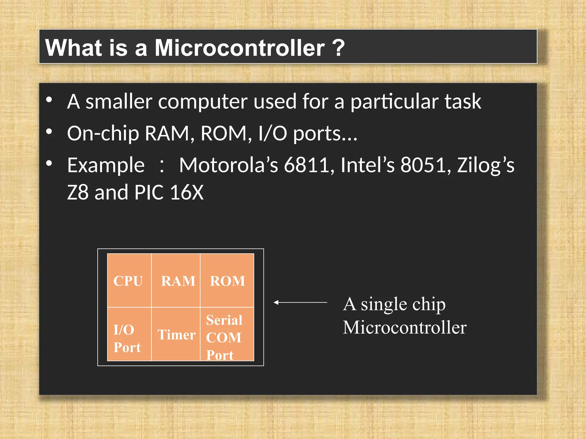
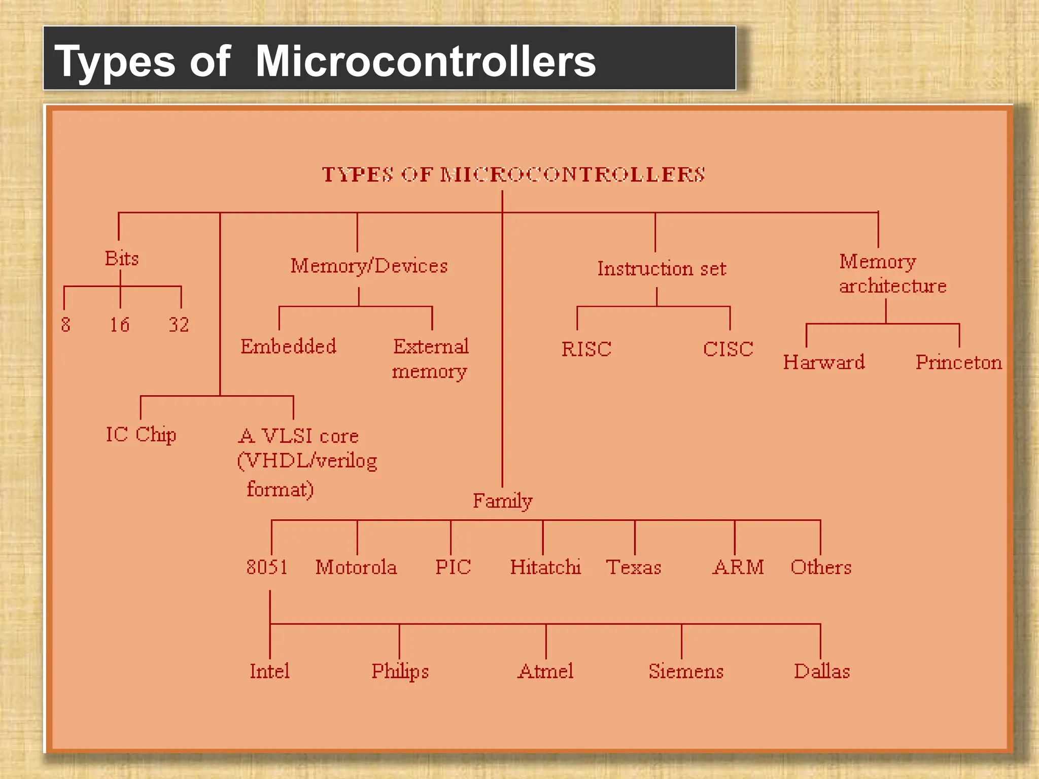
What is aMicrocontroller ? • A smaller computer used for a particular task • On-chip RAM, ROM, I/O ports... • Example : Motorola’s 6811, Intel’s 8051, Zilog’s Z8 and PIC 16X RAM ROM I/O Port Timer Serial COM Port CPU A single chip Microcontroller
3.
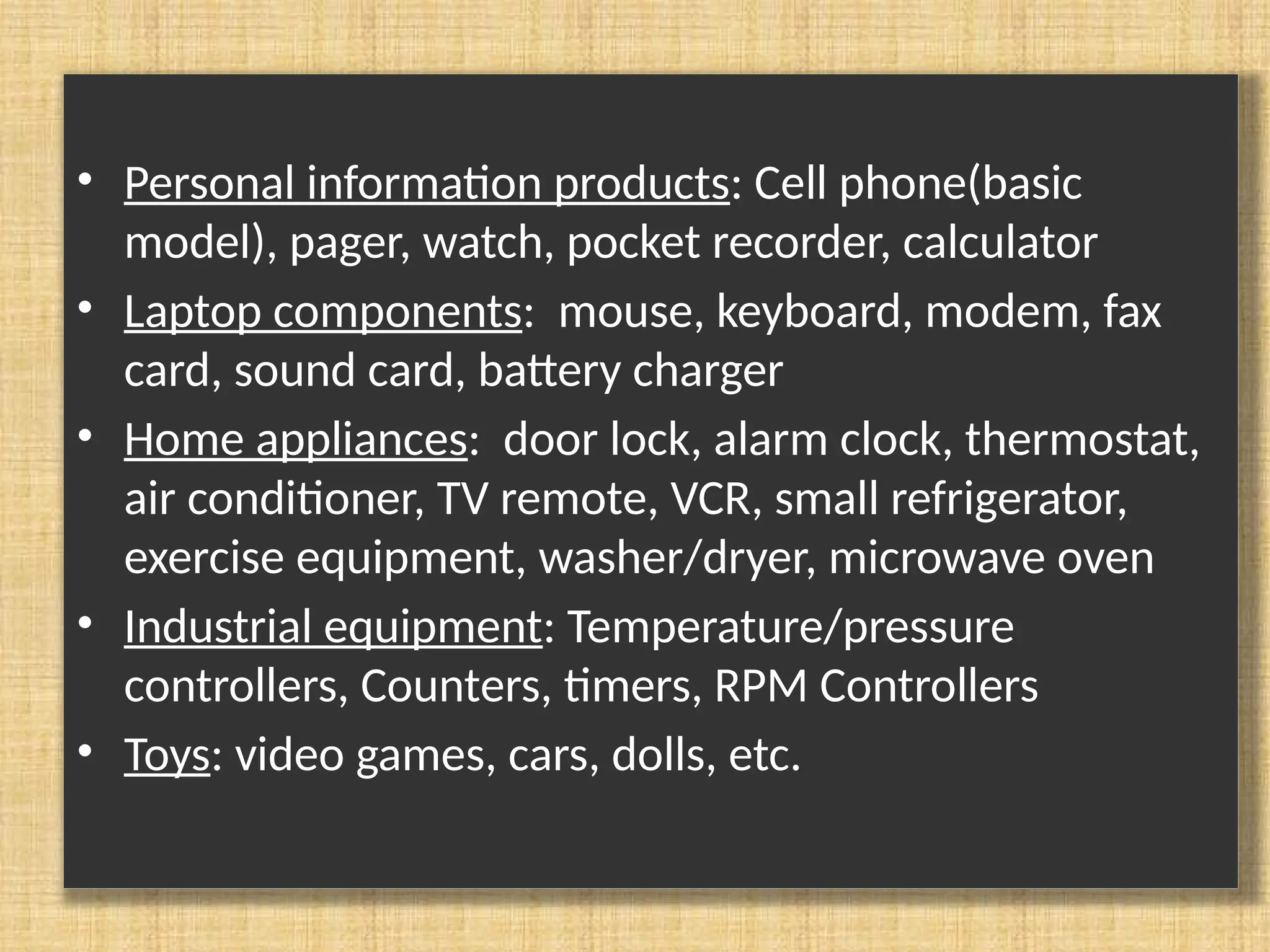
• Personal informationproducts: Cell phone(basic model), pager, watch, pocket recorder, calculator • Laptop components: mouse, keyboard, modem, fax card, sound card, battery charger • Home appliances: door lock, alarm clock, thermostat, air conditioner, TV remote, VCR, small refrigerator, exercise equipment, washer/dryer, microwave oven • Industrial equipment: Temperature/pressure controllers, Counters, timers, RPM Controllers • Toys: video games, cars, dolls, etc.
4.
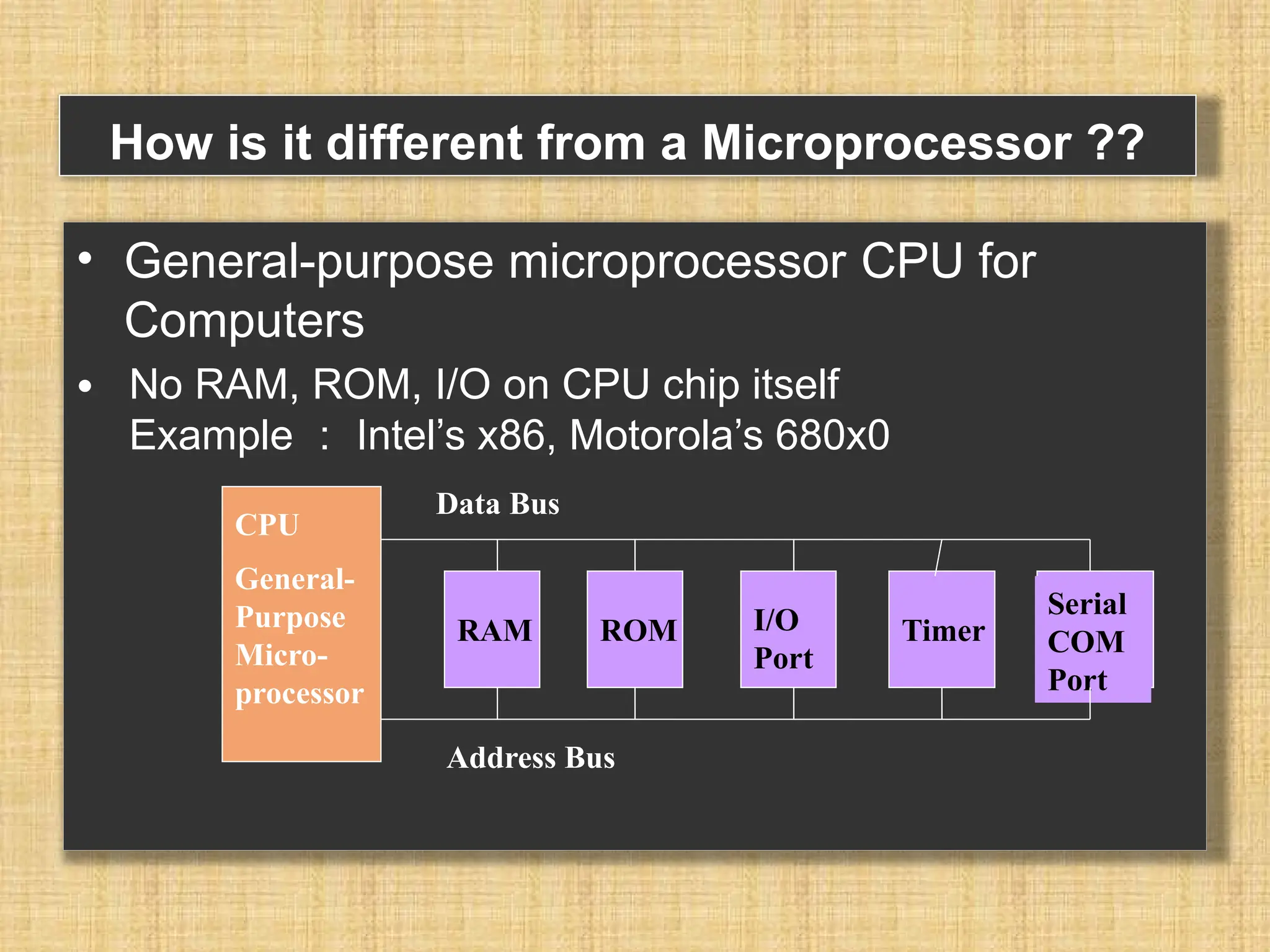
How is itdifferent from a Microprocessor ?? • General-purpose microprocessor CPU for Computers • No RAM, ROM, I/O on CPU chip itself Example : Intel’s x86, Motorola’s 680x0 CPU General- Purpose Micro- processor RAM ROM I/O Port Timer Serial COM Port Data Bus Address Bus
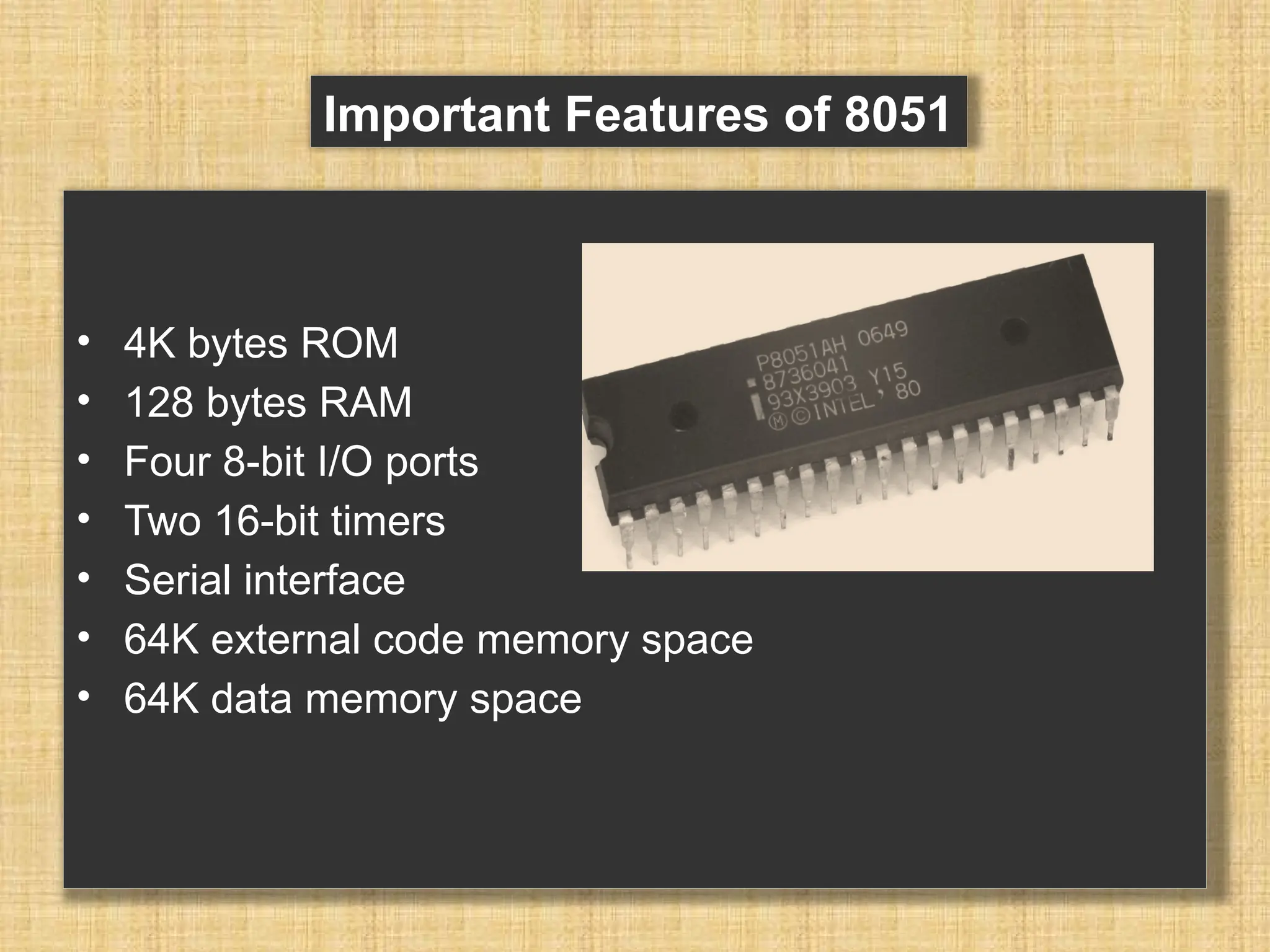
• 4K bytesROM • 128 bytes RAM • Four 8-bit I/O ports • Two 16-bit timers • Serial interface • 64K external code memory space • 64K data memory space Important Features of 8051
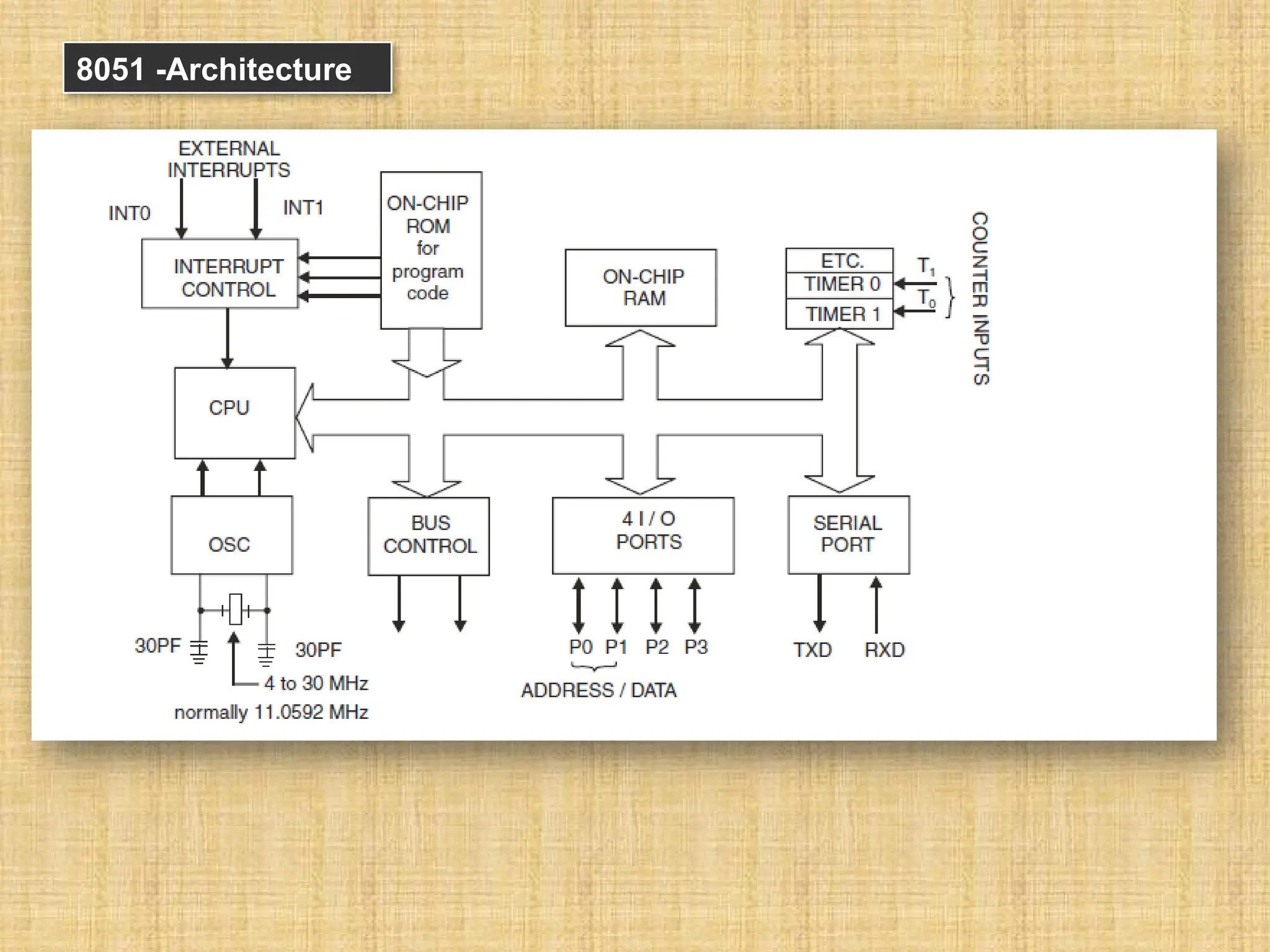
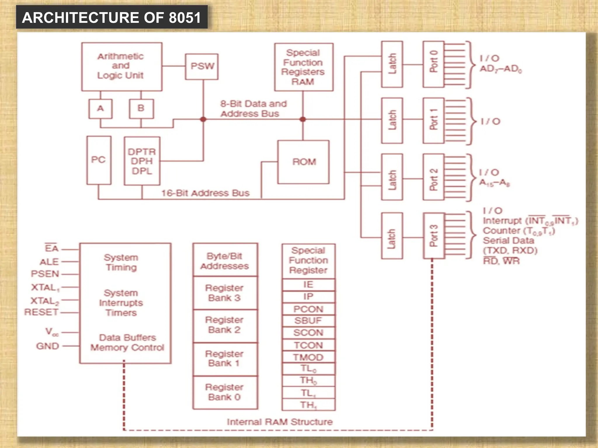
PC: program counter (whichpoints the next instruction to be executed) Oscillator • It is used for providing the clock to MC8051 which decides the speed or baud rate of MC. • We use crystal which frequency vary from 4MHz to 30 MHz, normally we use 11.0592 MHz frequency. Interrupts • Interrupts are defined as requests because they can be refused (masked) if they are not used, that is when an interrupt is acknowledged. A special set of events or routines are followed to handle the interrupts. These special routines are known as interrupt handler or interrupt service routines (ISR). These are located at a special location in memory. • INT0 and INT1 are the pins for external interrupts.
13.
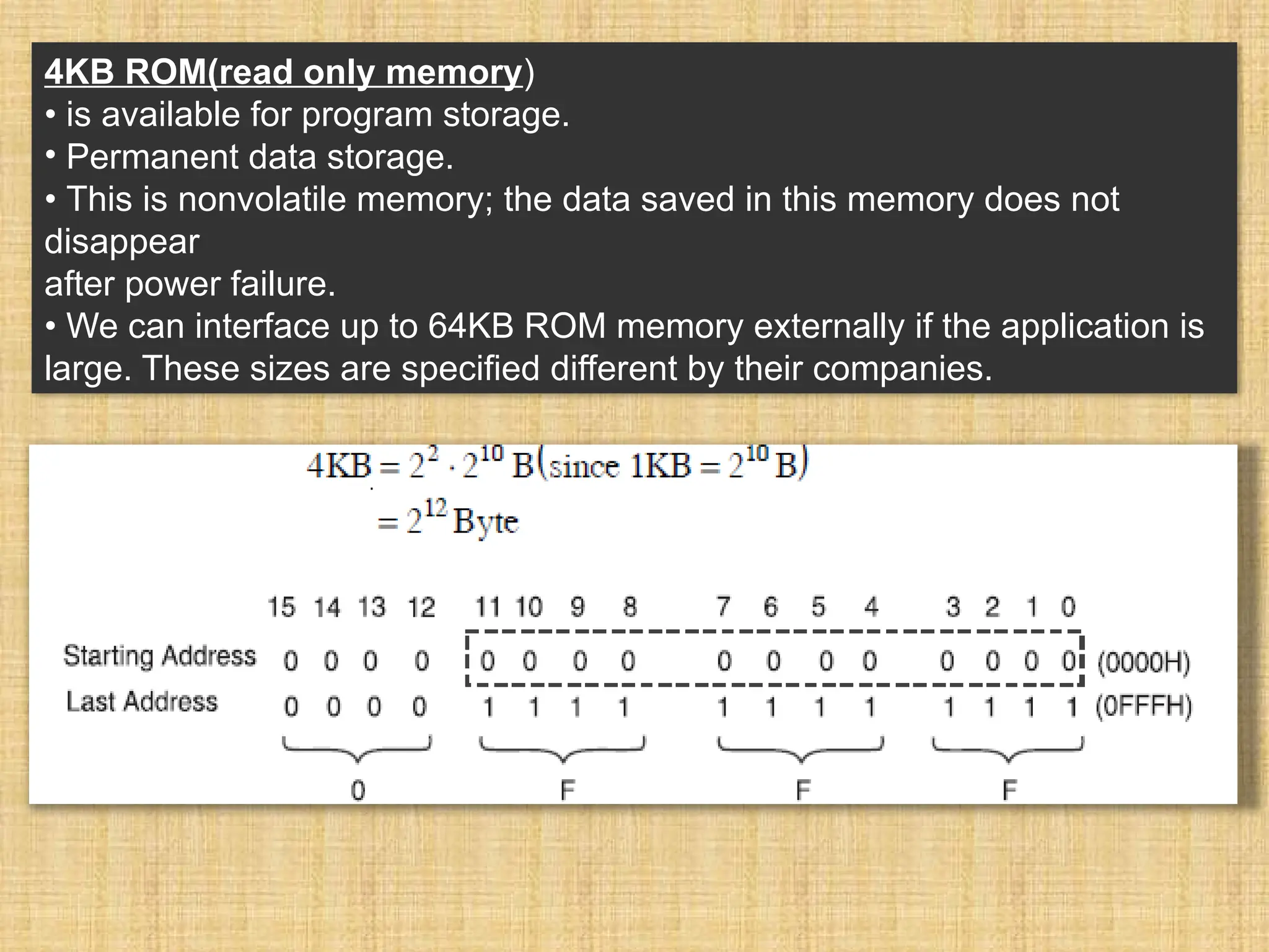
4KB ROM(read onlymemory) • is available for program storage. • Permanent data storage. • This is nonvolatile memory; the data saved in this memory does not disappear after power failure. • We can interface up to 64KB ROM memory externally if the application is large. These sizes are specified different by their companies.
14.
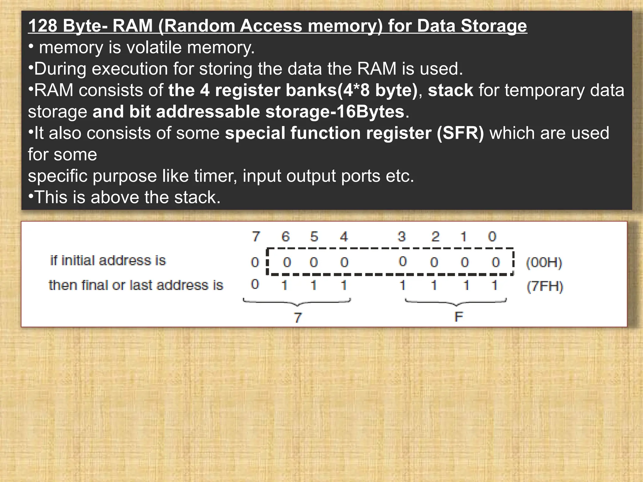
128 Byte- RAM(Random Access memory) for Data Storage • memory is volatile memory. •During execution for storing the data the RAM is used. •RAM consists of the 4 register banks(4*8 byte), stack for temporary data storage and bit addressable storage-16Bytes. •It also consists of some special function register (SFR) which are used for some specific purpose like timer, input output ports etc. •This is above the stack.
15.
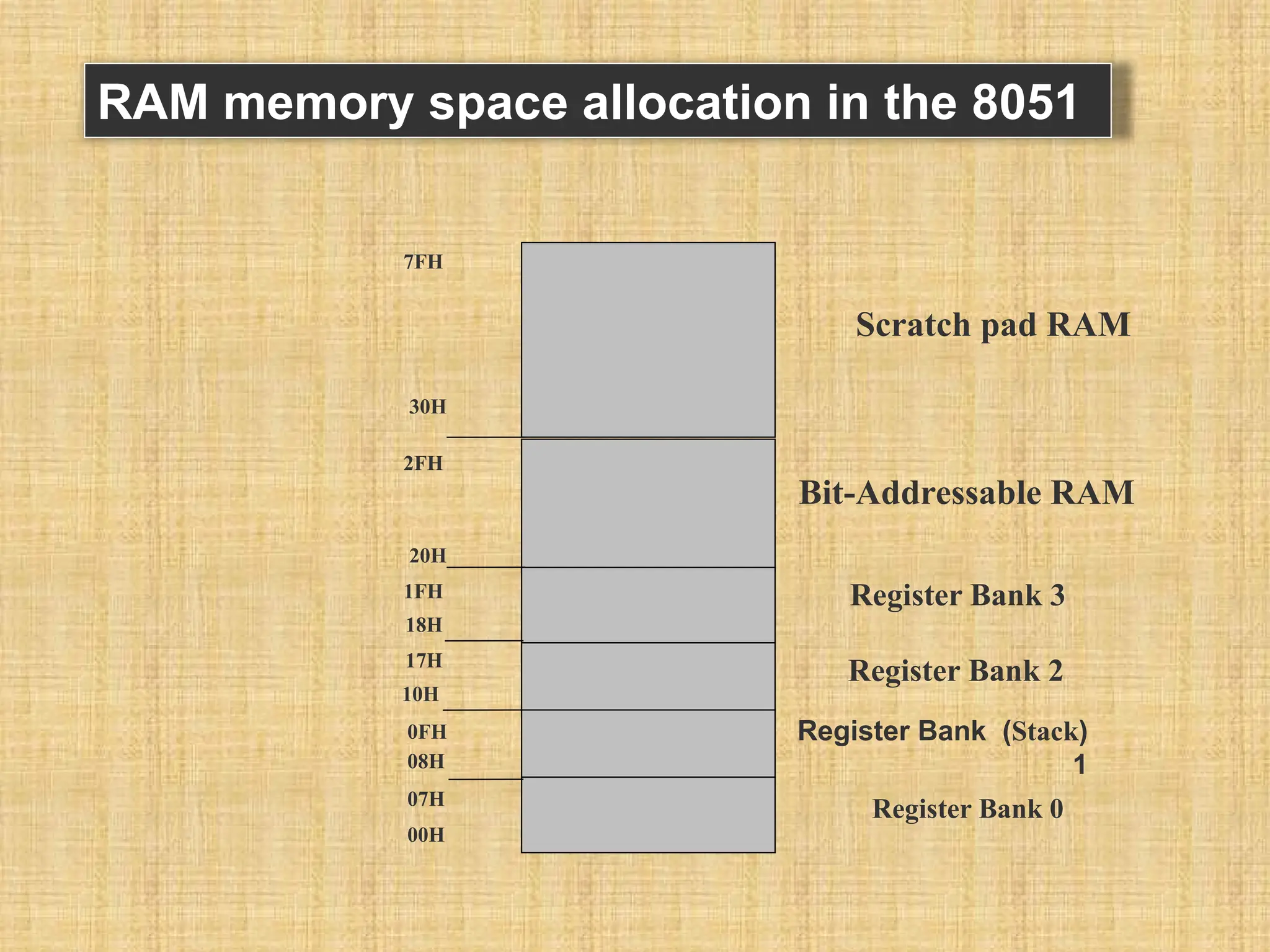
RAM memory spaceallocation in the 8051 7FH 30H 2FH 20H 1FH 17H 10H 0FH 07H 08H 18H 00H Register Bank 0 ( Stack ) Register Bank 1 Register Bank 2 Register Bank 3 Bit-Addressable RAM Scratch pad RAM
Serial Port • Thereare two pins available for serial communication TXD and RXD. • Normally TXD is used for transmitting serial data which is in SBUF register, RXD is used for receiving the serial data. • SCON register is used for controlling the operation
18.
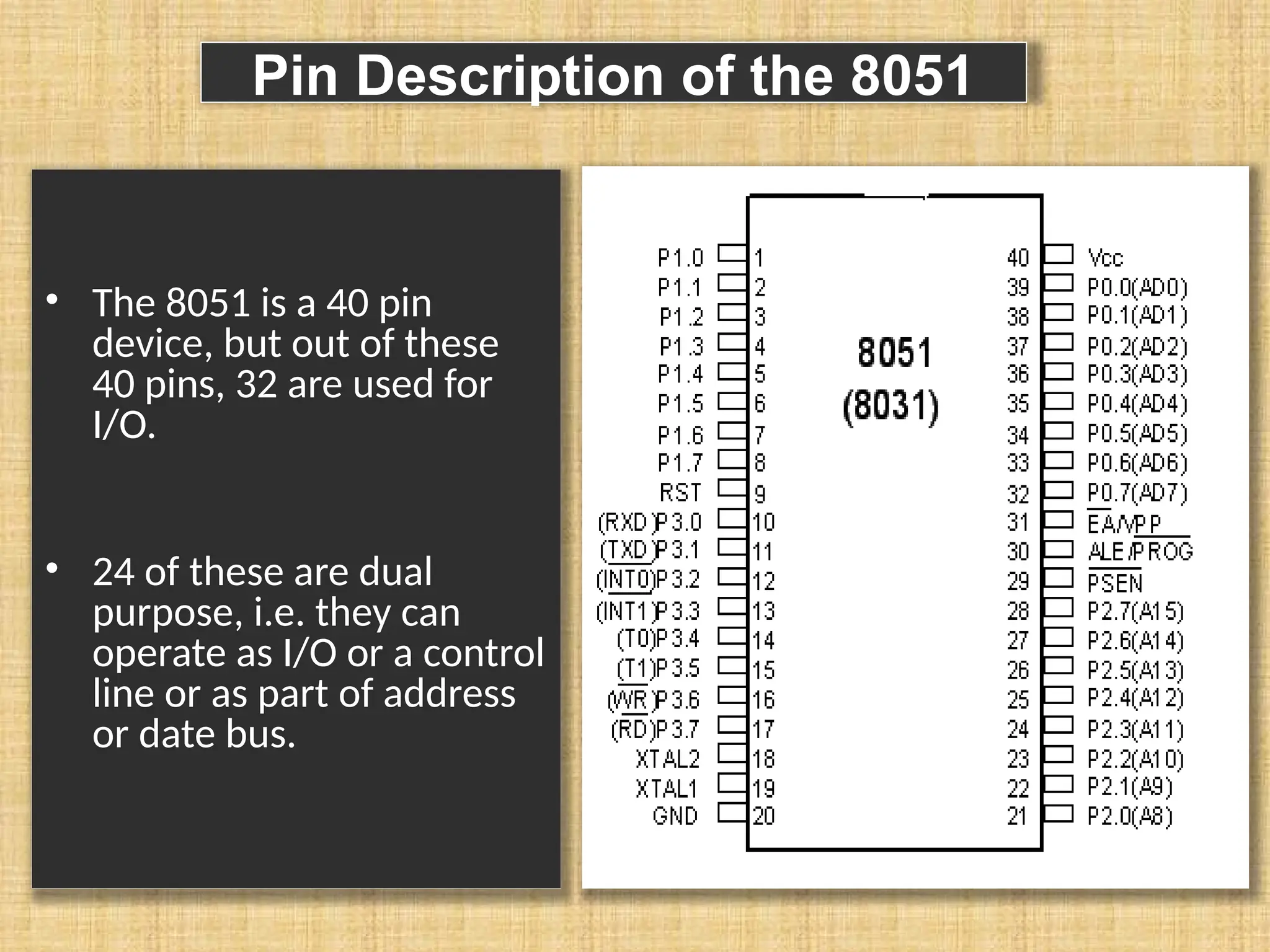
Pin Description ofthe 8051 • The 8051 is a 40 pin device, but out of these 40 pins, 32 are used for I/O. • 24 of these are dual purpose, i.e. they can operate as I/O or a control line or as part of address or date bus.
19.
Input Output Ports •four input output ports P0, P1, P2, P3. • Each port is 8 bit wide and has special function register P0, P1, P2, P3 which are bit addressable means each bit can be set or reset by the Bit instructions (SETB for high, CLR for low) independently. • The data at any port which is transmitting or receiving is in these registers. • The port 0 can perform dual works. It is also used as Lower order address bus (A0 to A7) multiplexed with 8 bit data bus P0.0 to P0.7 is AD0 to AD7 respectively the address bus and data bus is demultiplex by the ALE signal and latch which is further discussed in details. • Port 2 can be used as I/O port as well as higher order address bus A8 to A15.
20.
• Port 3also have dual functions it can be worked as I/O as well as each pin of P3 has specific function. P3.0 – RXD – {Serial I / P for Asynchronous communication & Serial O / P for synchronous communication.} P3.1 – TXD – Serial data transmit. P3.2 – INT0 – External Interrupt 0. P3.3 – INT1 – External Interrupt 1. P3.4 – T0 – Clock input for counter 0. P3.5 – T1 – Clock input for counter 1. P3.6 – WR – Signal for writing to external memory. P3.7 – RD – Signal for reading from external memory. When external memory is interfaced with 8051 then P0 and P2 can’t be worked as I/O port they works as address bus and data bus, otherwise they can be accessed as I/O ports.
21.
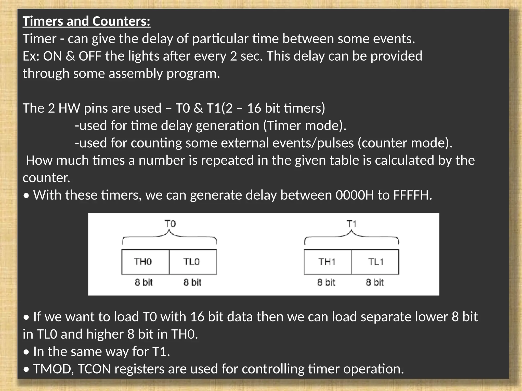
Timers and Counters: Timer- can give the delay of particular time between some events. Ex: ON & OFF the lights after every 2 sec. This delay can be provided through some assembly program. The 2 HW pins are used – T0 & T1(2 – 16 bit timers) -used for time delay generation (Timer mode). -used for counting some external events/pulses (counter mode). How much times a number is repeated in the given table is calculated by the counter. • With these timers, we can generate delay between 0000H to FFFFH. • If we want to load T0 with 16 bit data then we can load separate lower 8 bit in TL0 and higher 8 bit in TH0. • In the same way for T1. • TMOD, TCON registers are used for controlling timer operation.
22.
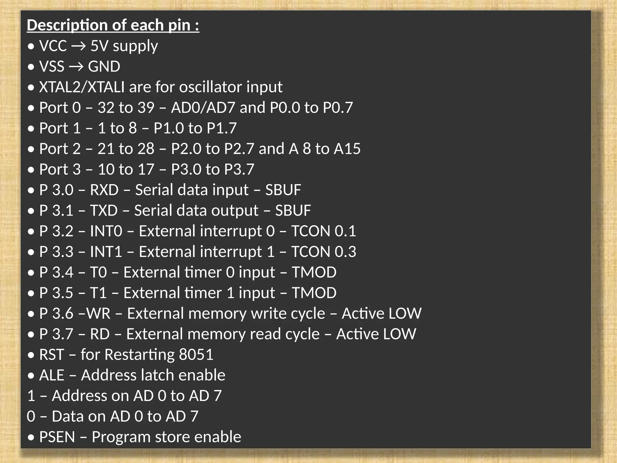
Description of eachpin : • VCC → 5V supply • VSS → GND • XTAL2/XTALI are for oscillator input • Port 0 – 32 to 39 – AD0/AD7 and P0.0 to P0.7 • Port 1 – 1 to 8 – P1.0 to P1.7 • Port 2 – 21 to 28 – P2.0 to P2.7 and A 8 to A15 • Port 3 – 10 to 17 – P3.0 to P3.7 • P 3.0 – RXD – Serial data input – SBUF • P 3.1 – TXD – Serial data output – SBUF • P 3.2 – INT0 – External interrupt 0 – TCON 0.1 • P 3.3 – INT1 – External interrupt 1 – TCON 0.3 • P 3.4 – T0 – External timer 0 input – TMOD • P 3.5 – T1 – External timer 1 input – TMOD • P 3.6 –WR – External memory write cycle – Active LOW • P 3.7 – RD – External memory read cycle – Active LOW • RST – for Restarting 8051 • ALE – Address latch enable 1 – Address on AD 0 to AD 7 0 – Data on AD 0 to AD 7 • PSEN – Program store enable
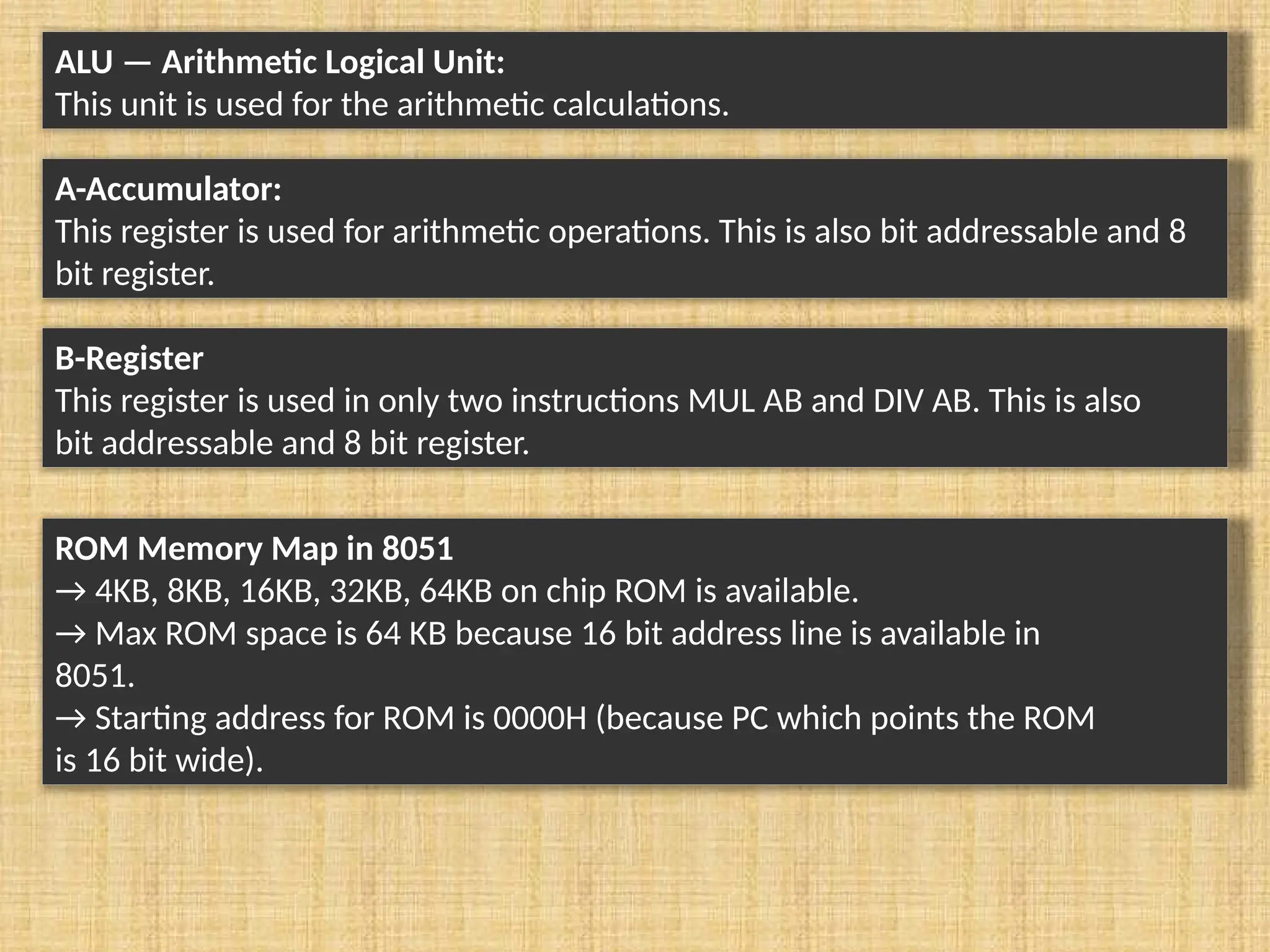
ALU — ArithmeticLogical Unit: This unit is used for the arithmetic calculations. A-Accumulator: This register is used for arithmetic operations. This is also bit addressable and 8 bit register. B-Register This register is used in only two instructions MUL AB and DIV AB. This is also bit addressable and 8 bit register. ROM Memory Map in 8051 → 4KB, 8KB, 16KB, 32KB, 64KB on chip ROM is available. → Max ROM space is 64 KB because 16 bit address line is available in 8051. → Starting address for ROM is 0000H (because PC which points the ROM is 16 bit wide).
25.
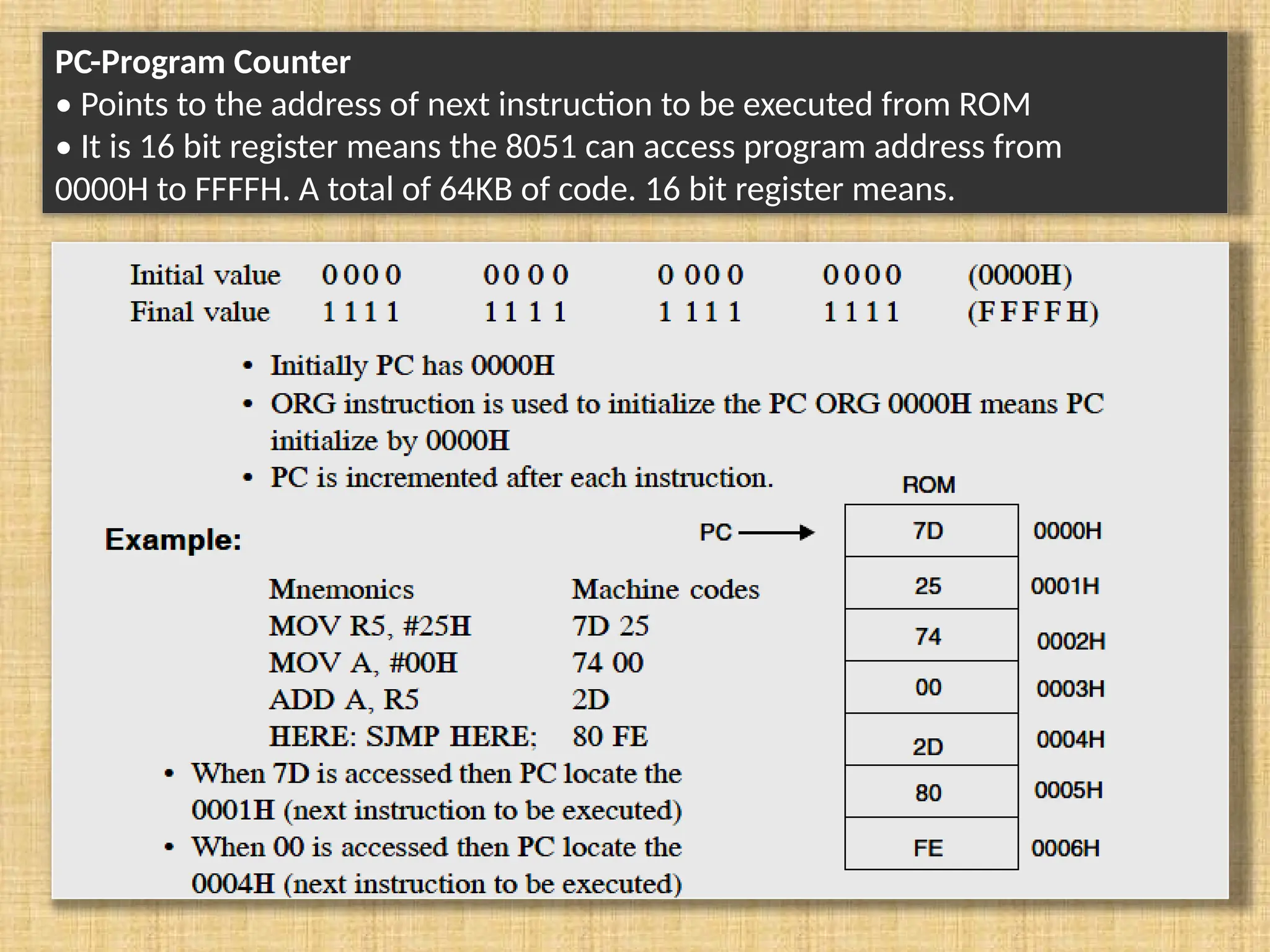
PC-Program Counter • Pointsto the address of next instruction to be executed from ROM • It is 16 bit register means the 8051 can access program address from 0000H to FFFFH. A total of 64KB of code. 16 bit register means.
26.
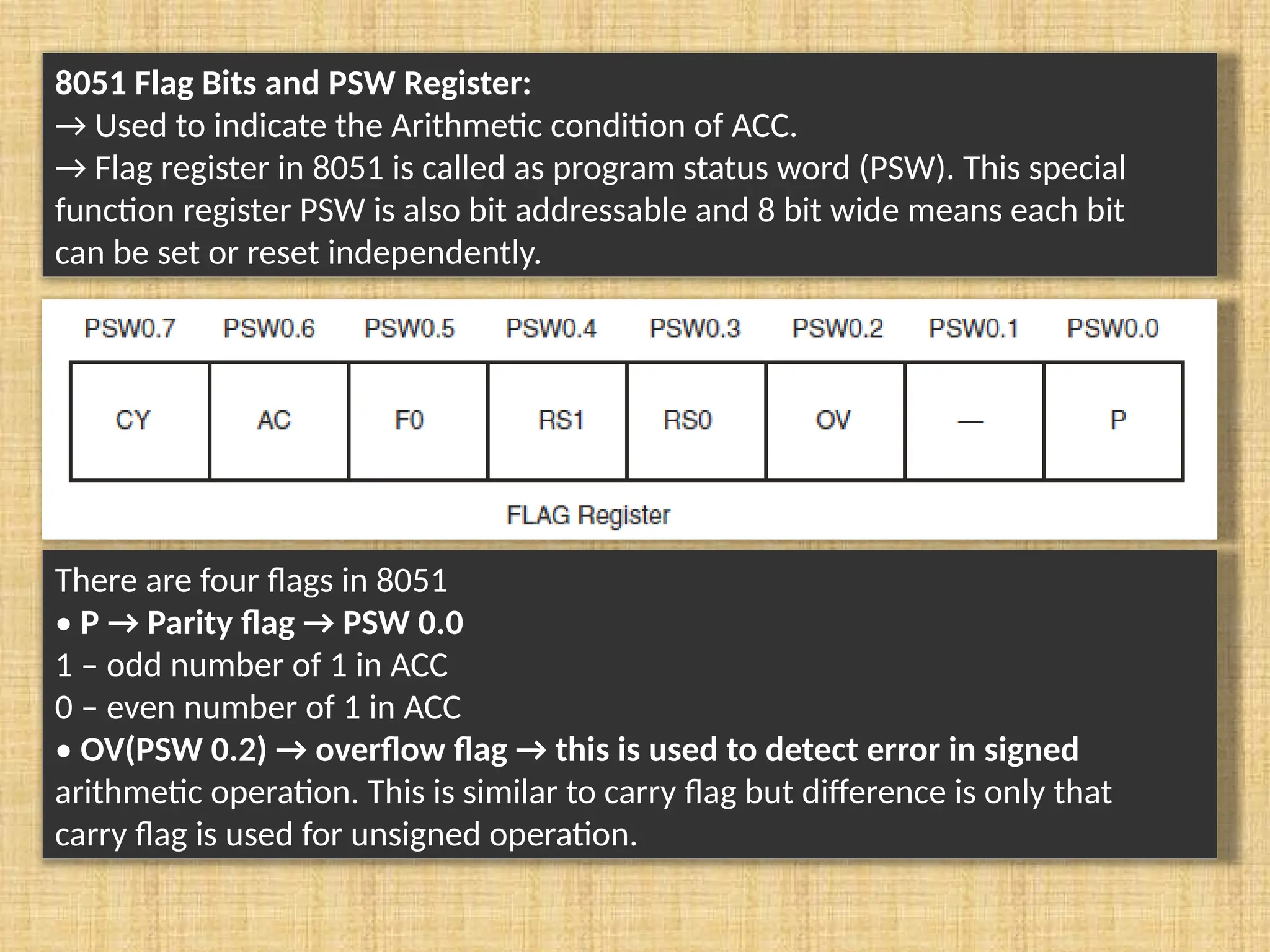
8051 Flag Bitsand PSW Register: → Used to indicate the Arithmetic condition of ACC. → Flag register in 8051 is called as program status word (PSW). This special function register PSW is also bit addressable and 8 bit wide means each bit can be set or reset independently. There are four flags in 8051 • P → Parity flag → PSW 0.0 1 – odd number of 1 in ACC 0 – even number of 1 in ACC • OV(PSW 0.2) → overflow flag → this is used to detect error in signed arithmetic operation. This is similar to carry flag but difference is only that carry flag is used for unsigned operation.
27.
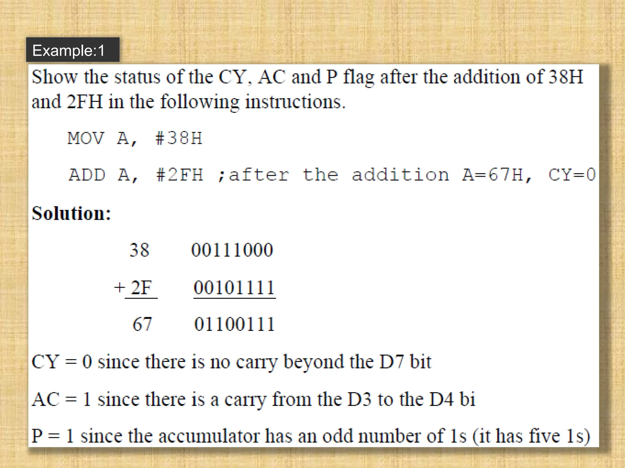
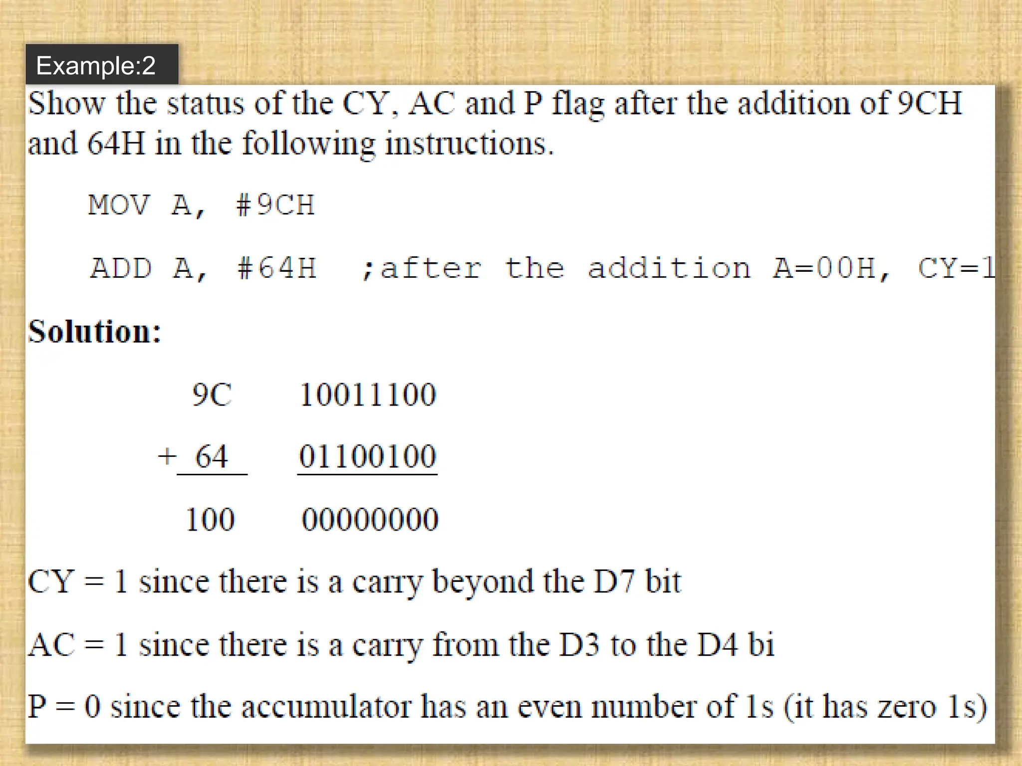
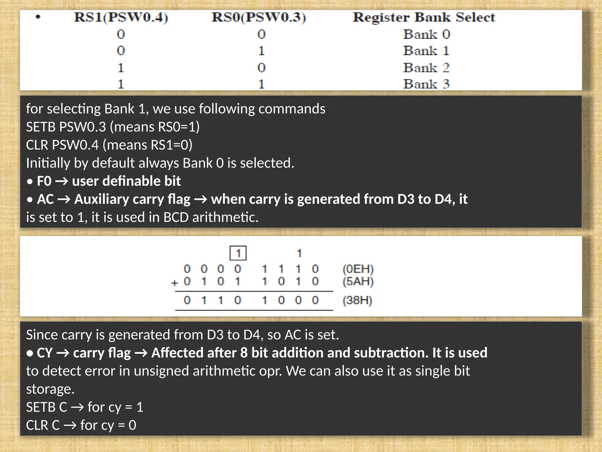
for selecting Bank1, we use following commands SETB PSW0.3 (means RS0=1) CLR PSW0.4 (means RS1=0) Initially by default always Bank 0 is selected. • F0 → user definable bit • AC → Auxiliary carry flag → when carry is generated from D3 to D4, it is set to 1, it is used in BCD arithmetic. Since carry is generated from D3 to D4, so AC is set. • CY → carry flag → Affected after 8 bit addition and subtraction. It is used to detect error in unsigned arithmetic opr. We can also use it as single bit storage. SETB C → for cy = 1 CLR C → for cy = 0
28.
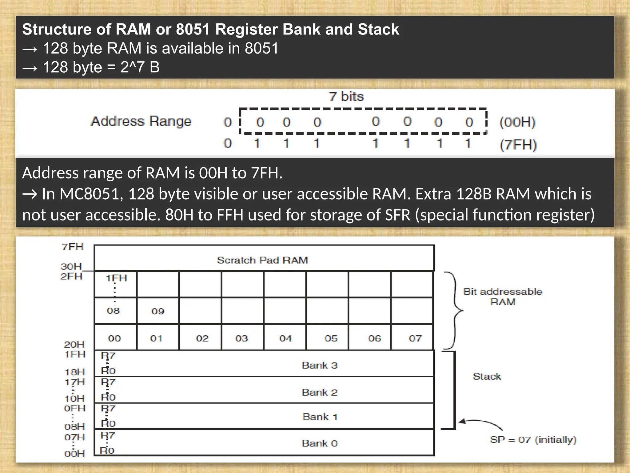
Structure of RAMor 8051 Register Bank and Stack → 128 byte RAM is available in 8051 → 128 byte = 2^7 B Address range of RAM is 00H to 7FH. → In MC8051, 128 byte visible or user accessible RAM. Extra 128B RAM which is not user accessible. 80H to FFH used for storage of SFR (special function register)
30.
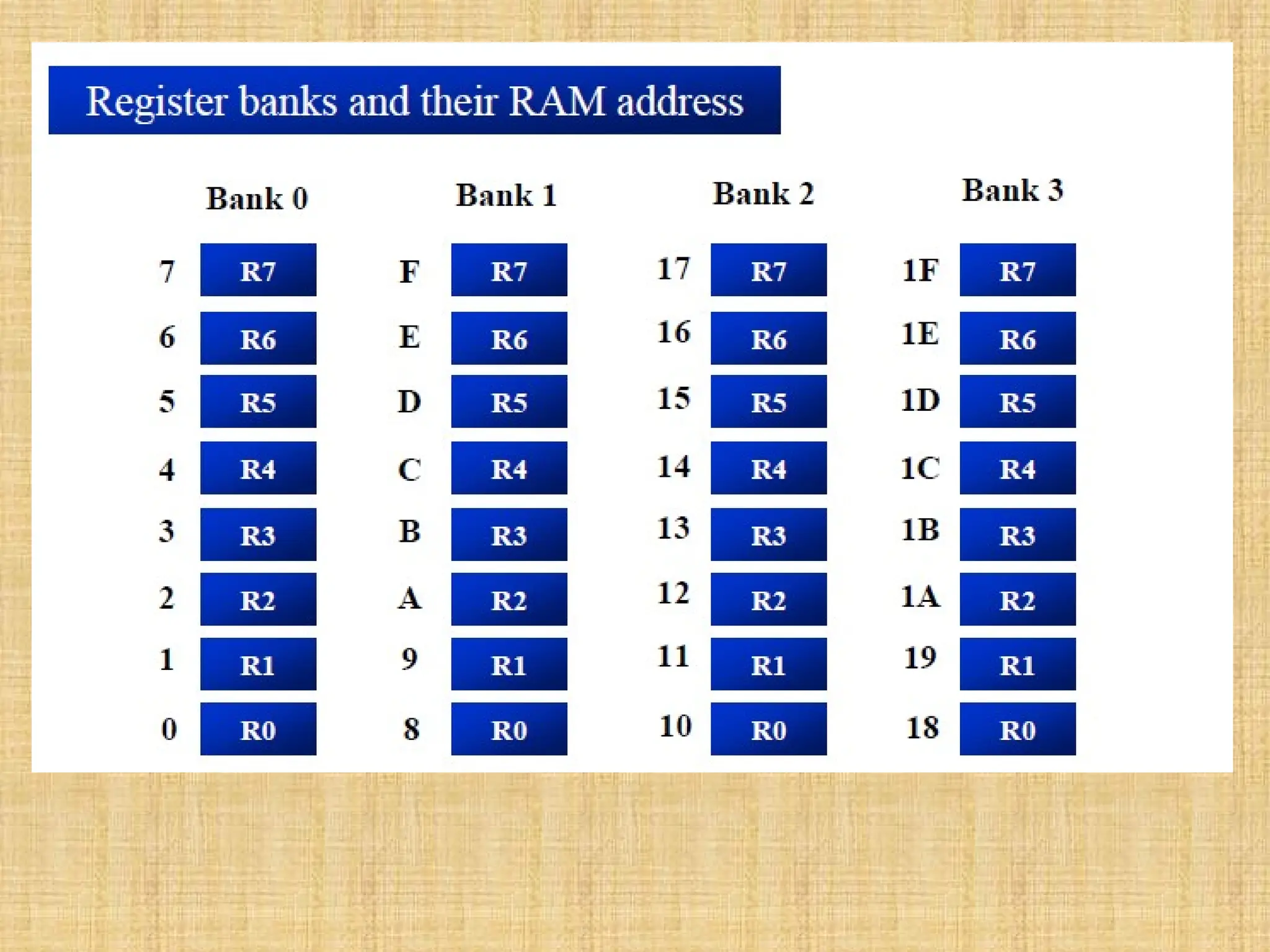
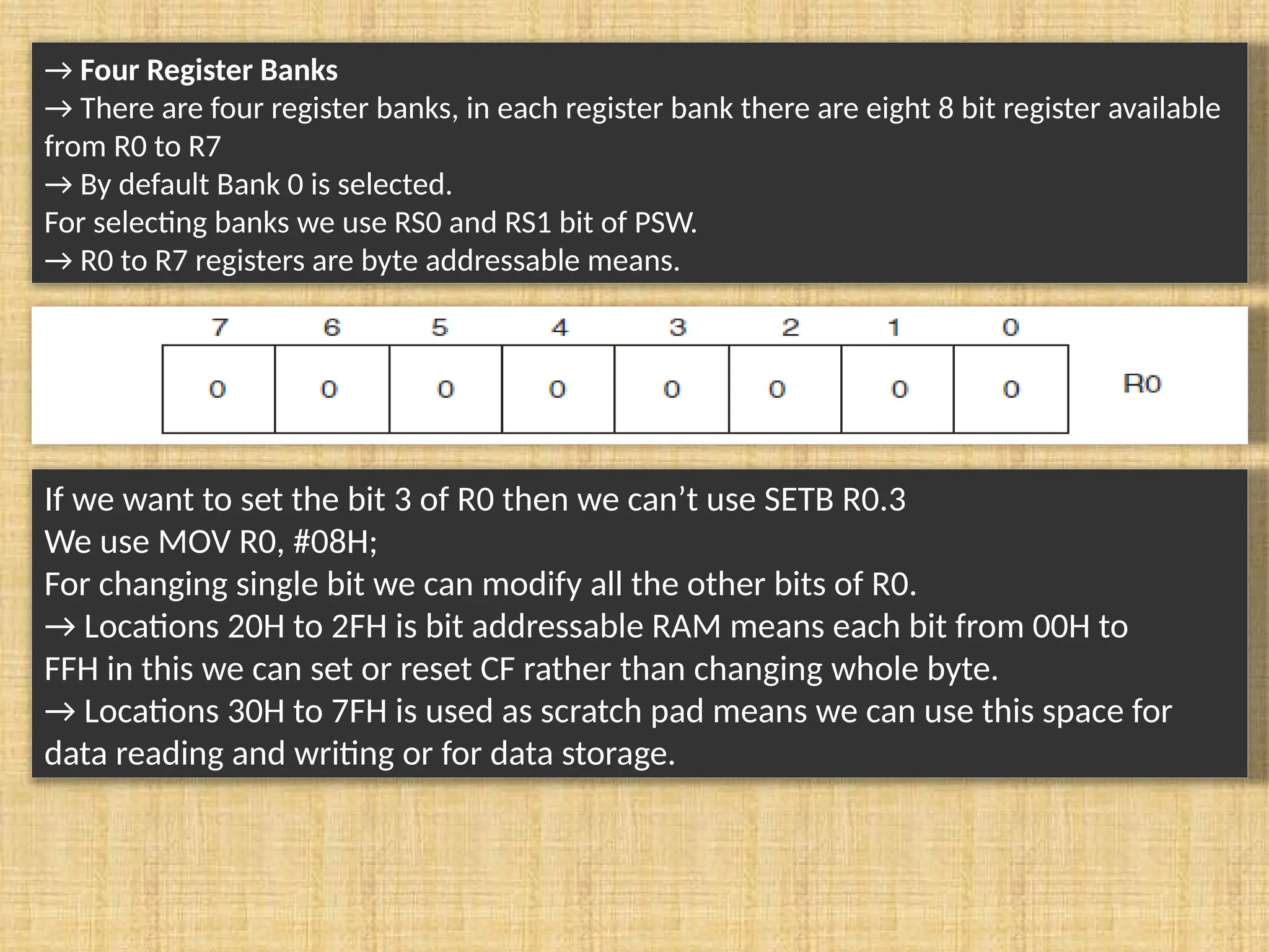
→ Four RegisterBanks → There are four register banks, in each register bank there are eight 8 bit register available from R0 to R7 → By default Bank 0 is selected. For selecting banks we use RS0 and RS1 bit of PSW. → R0 to R7 registers are byte addressable means. If we want to set the bit 3 of R0 then we can’t use SETB R0.3 We use MOV R0, #08H; For changing single bit we can modify all the other bits of R0. → Locations 20H to 2FH is bit addressable RAM means each bit from 00H to FFH in this we can set or reset CF rather than changing whole byte. → Locations 30H to 7FH is used as scratch pad means we can use this space for data reading and writing or for data storage.
31.
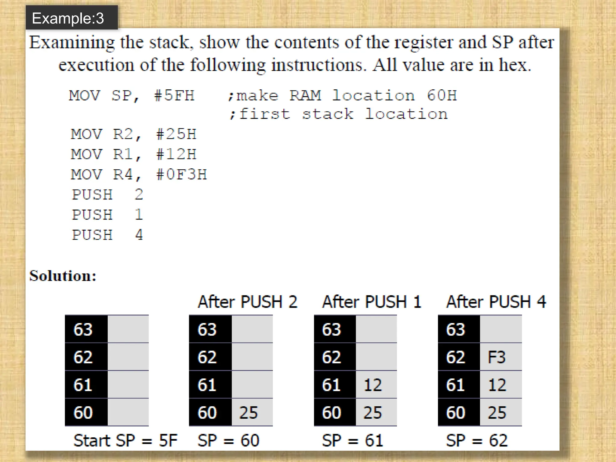
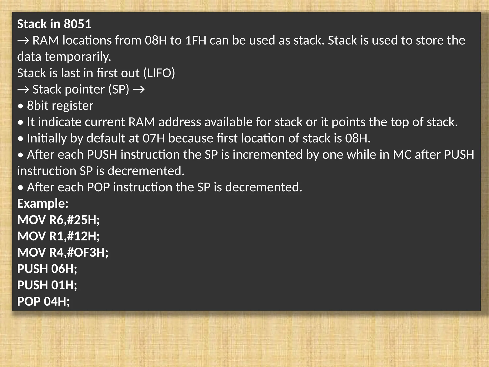
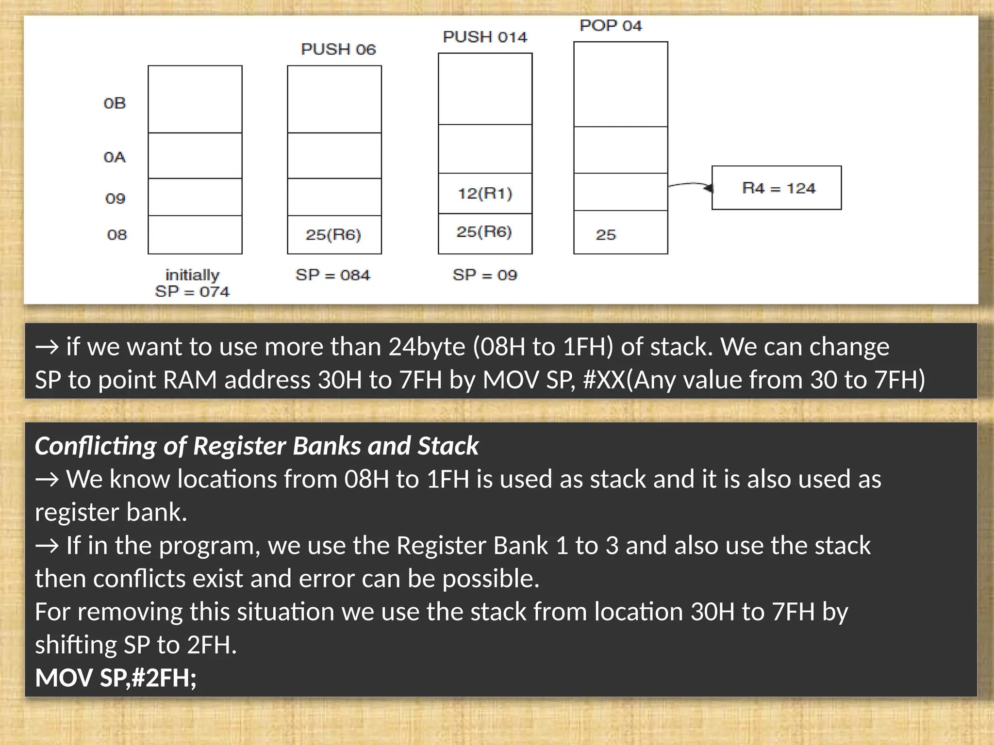
Stack in 8051 →RAM locations from 08H to 1FH can be used as stack. Stack is used to store the data temporarily. Stack is last in first out (LIFO) → Stack pointer (SP) → • 8bit register • It indicate current RAM address available for stack or it points the top of stack. • Initially by default at 07H because first location of stack is 08H. • After each PUSH instruction the SP is incremented by one while in MC after PUSH instruction SP is decremented. • After each POP instruction the SP is decremented. Example: MOV R6,#25H; MOV R1,#12H; MOV R4,#OF3H; PUSH 06H; PUSH 01H; POP 04H;
32.
→ if wewant to use more than 24byte (08H to 1FH) of stack. We can change SP to point RAM address 30H to 7FH by MOV SP, #XX(Any value from 30 to 7FH) Conflicting of Register Banks and Stack → We know locations from 08H to 1FH is used as stack and it is also used as register bank. → If in the program, we use the Register Bank 1 to 3 and also use the stack then conflicts exist and error can be possible. For removing this situation we use the stack from location 30H to 7FH by shifting SP to 2FH. MOV SP,#2FH;
33.
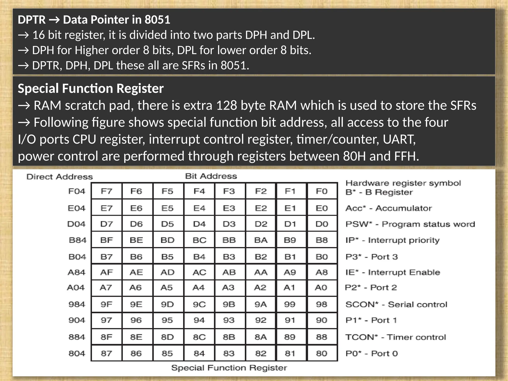
DPTR → DataPointer in 8051 → 16 bit register, it is divided into two parts DPH and DPL. → DPH for Higher order 8 bits, DPL for lower order 8 bits. → DPTR, DPH, DPL these all are SFRs in 8051. Special Function Register → RAM scratch pad, there is extra 128 byte RAM which is used to store the SFRs → Following figure shows special function bit address, all access to the four I/O ports CPU register, interrupt control register, timer/counter, UART, power control are performed through registers between 80H and FFH.
34.
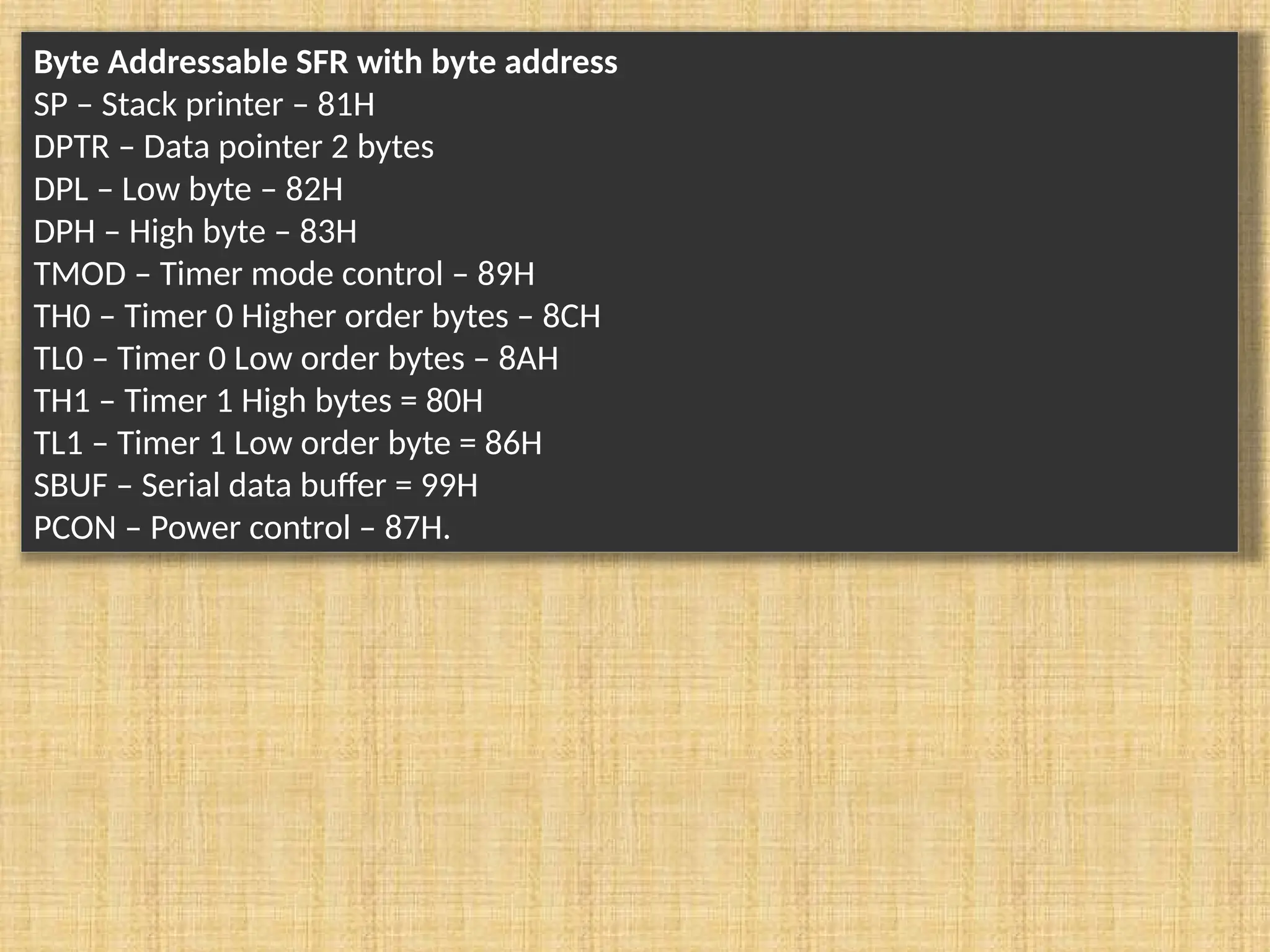
Byte Addressable SFRwith byte address SP – Stack printer – 81H DPTR – Data pointer 2 bytes DPL – Low byte – 82H DPH – High byte – 83H TMOD – Timer mode control – 89H TH0 – Timer 0 Higher order bytes – 8CH TL0 – Timer 0 Low order bytes – 8AH TH1 – Timer 1 High bytes = 80H TL1 – Timer 1 Low order byte = 86H SBUF – Serial data buffer = 99H PCON – Power control – 87H.
35.
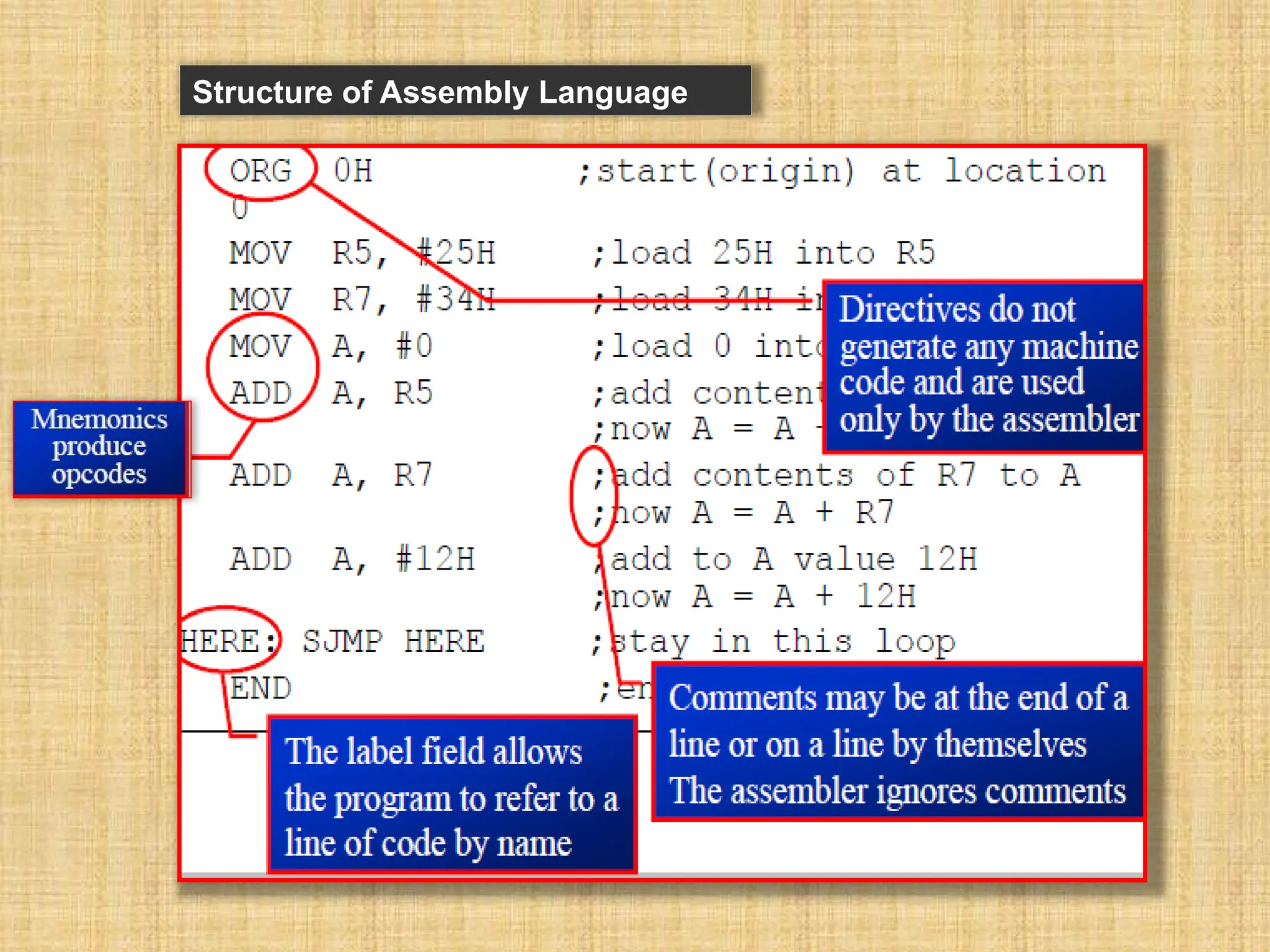
An Assembly languageinstruction consists of four fields: [label:] Mnemonic [operands] [;comment]
36.
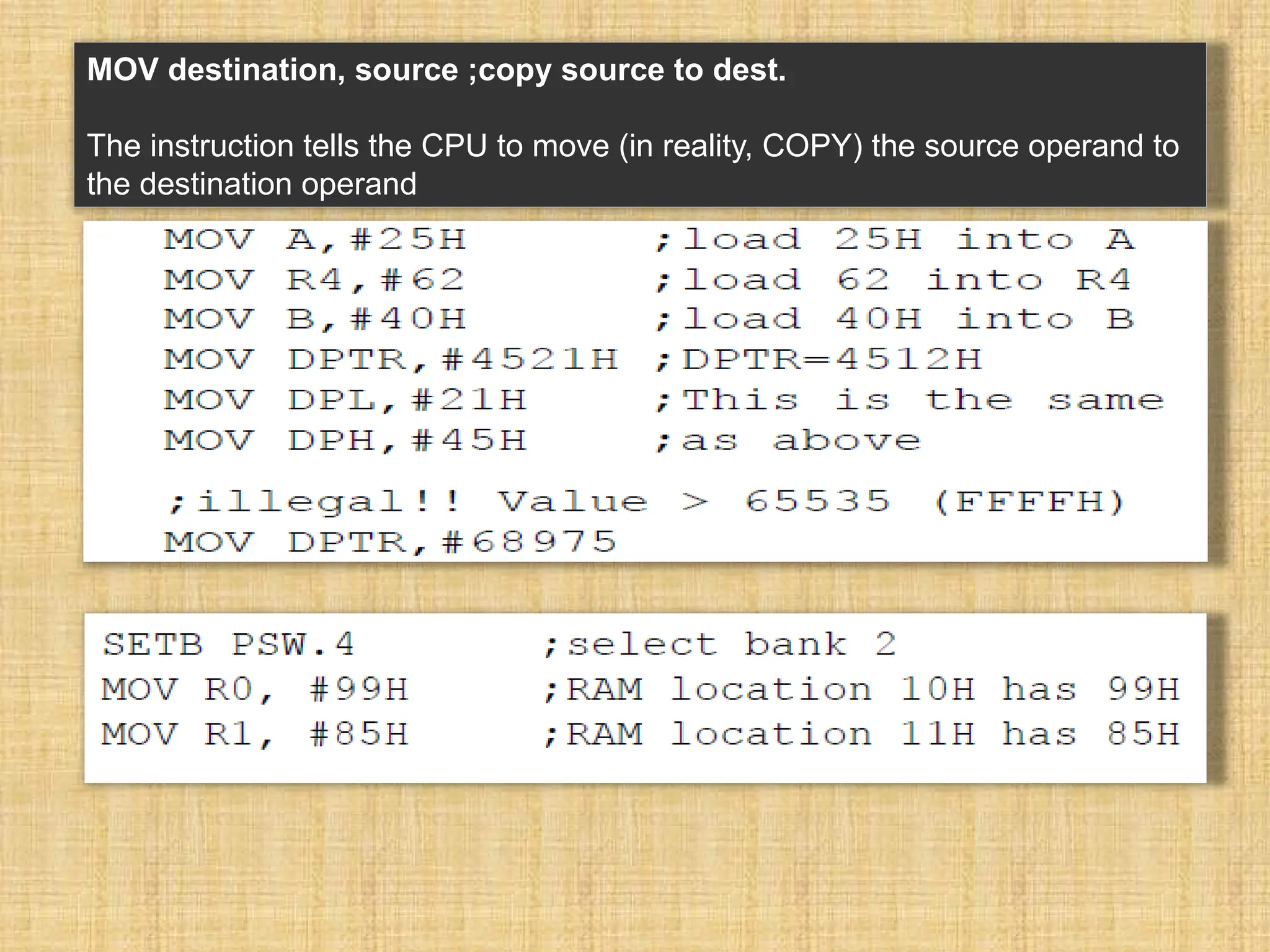
MOV destination, source;copy source to dest. The instruction tells the CPU to move (in reality, COPY) the source operand to the destination operand
37.
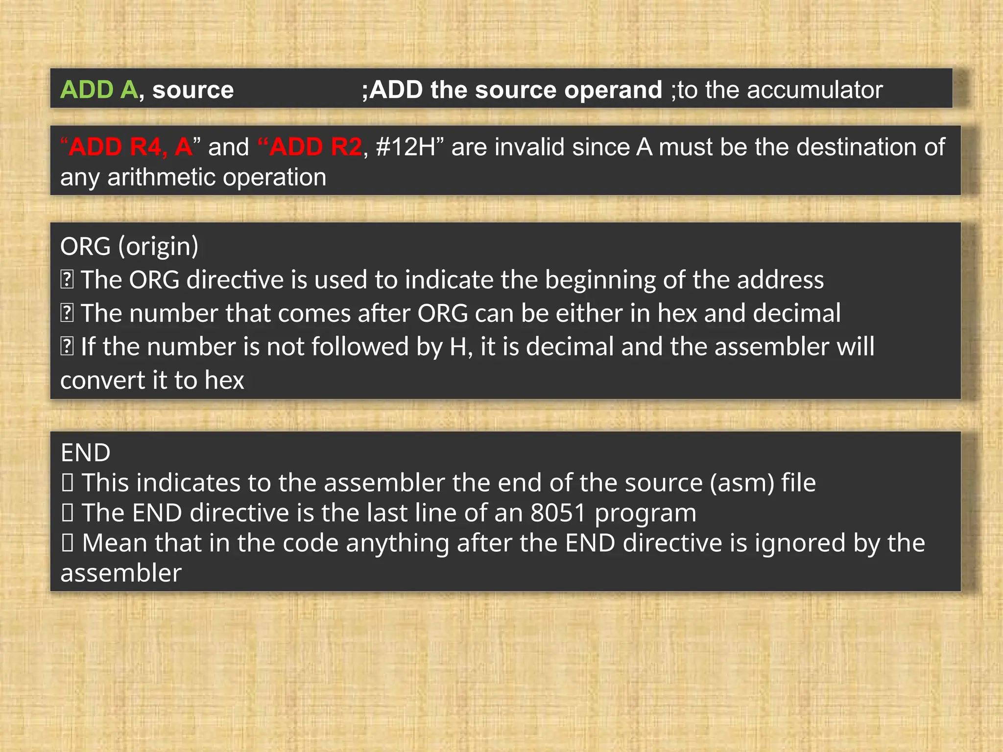
ADD A, source;ADD the source operand ;to the accumulator “ADD R4, A” and “ADD R2, #12H” are invalid since A must be the destination of any arithmetic operation ORG (origin) The ORG directive is used to indicate the beginning of the address The number that comes after ORG can be either in hex and decimal If the number is not followed by H, it is decimal and the assembler will convert it to hex END This indicates to the assembler the end of the source (asm) file The END directive is the last line of an 8051 program Mean that in the code anything after the END directive is ignored by the assembler
38.
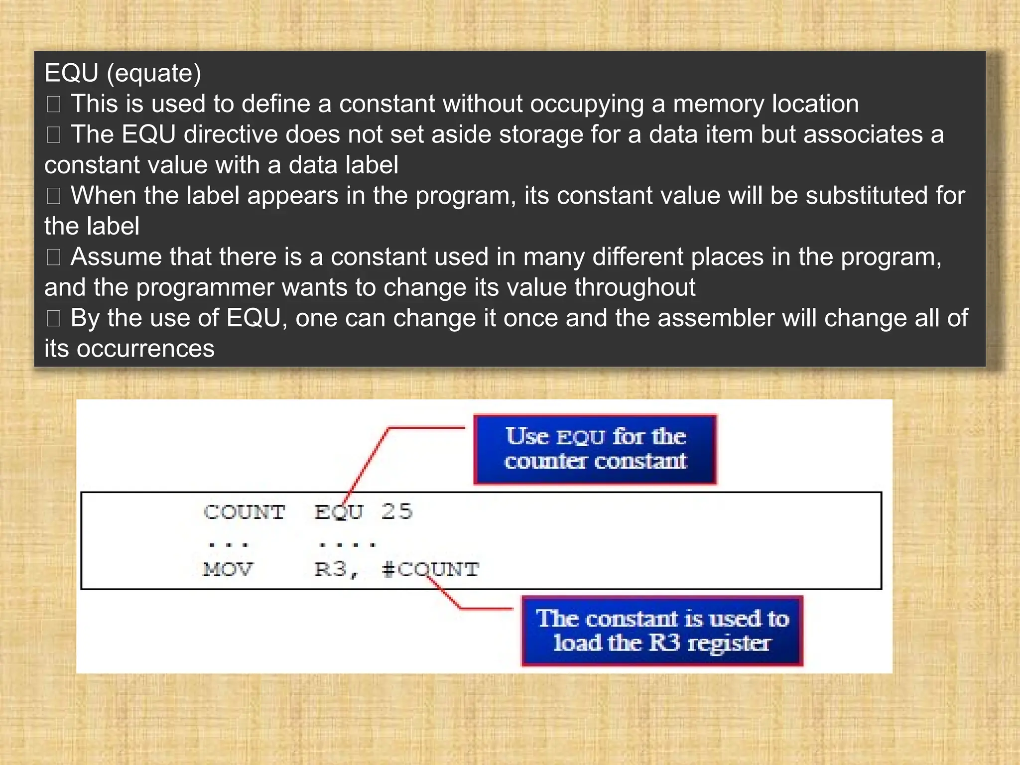
EQU (equate) Thisis used to define a constant without occupying a memory location The EQU directive does not set aside storage for a data item but associates a constant value with a data label When the label appears in the program, its constant value will be substituted for the label Assume that there is a constant used in many different places in the program, and the programmer wants to change its value throughout By the use of EQU, one can change it once and the assembler will change all of its occurrences
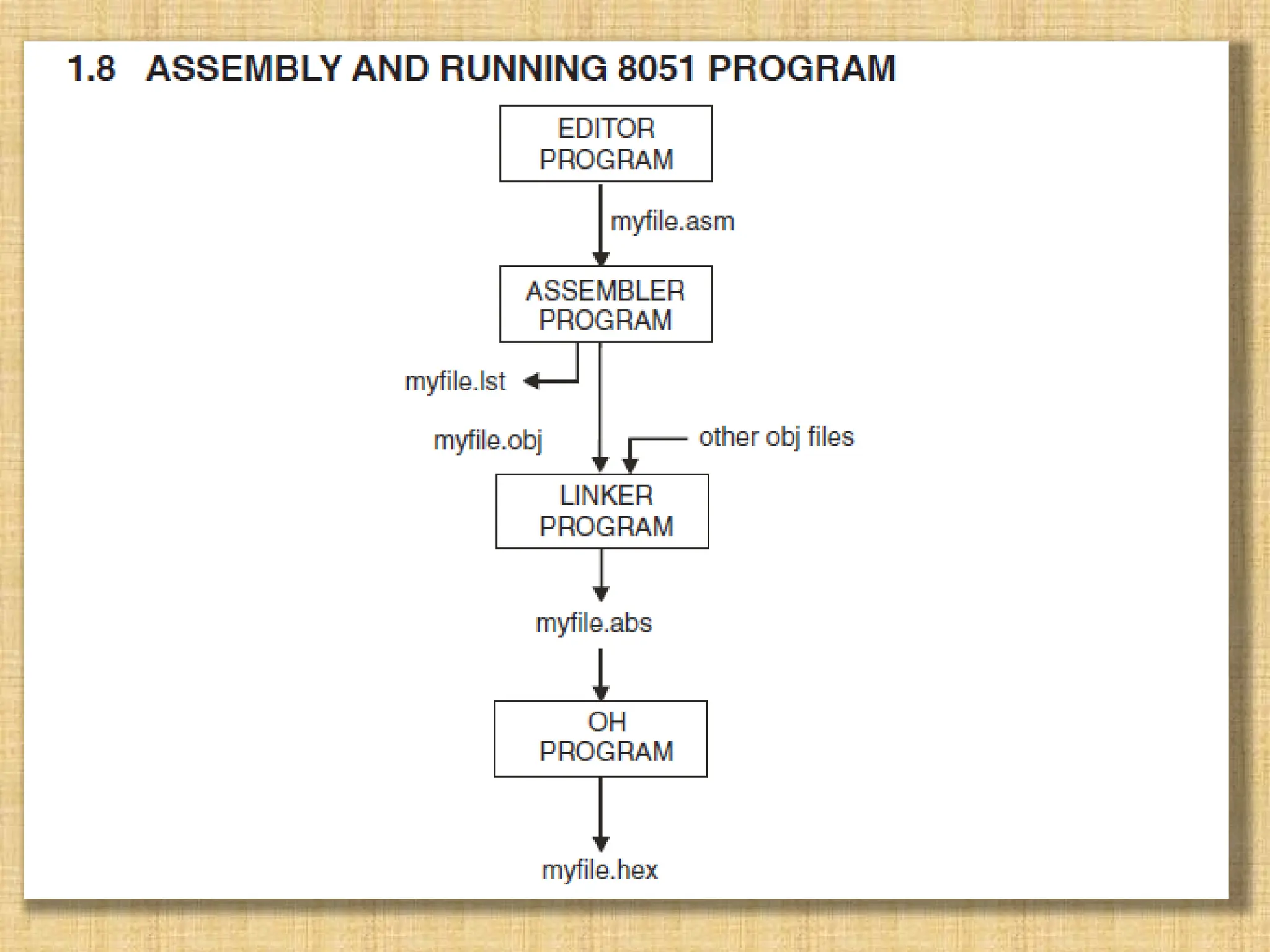
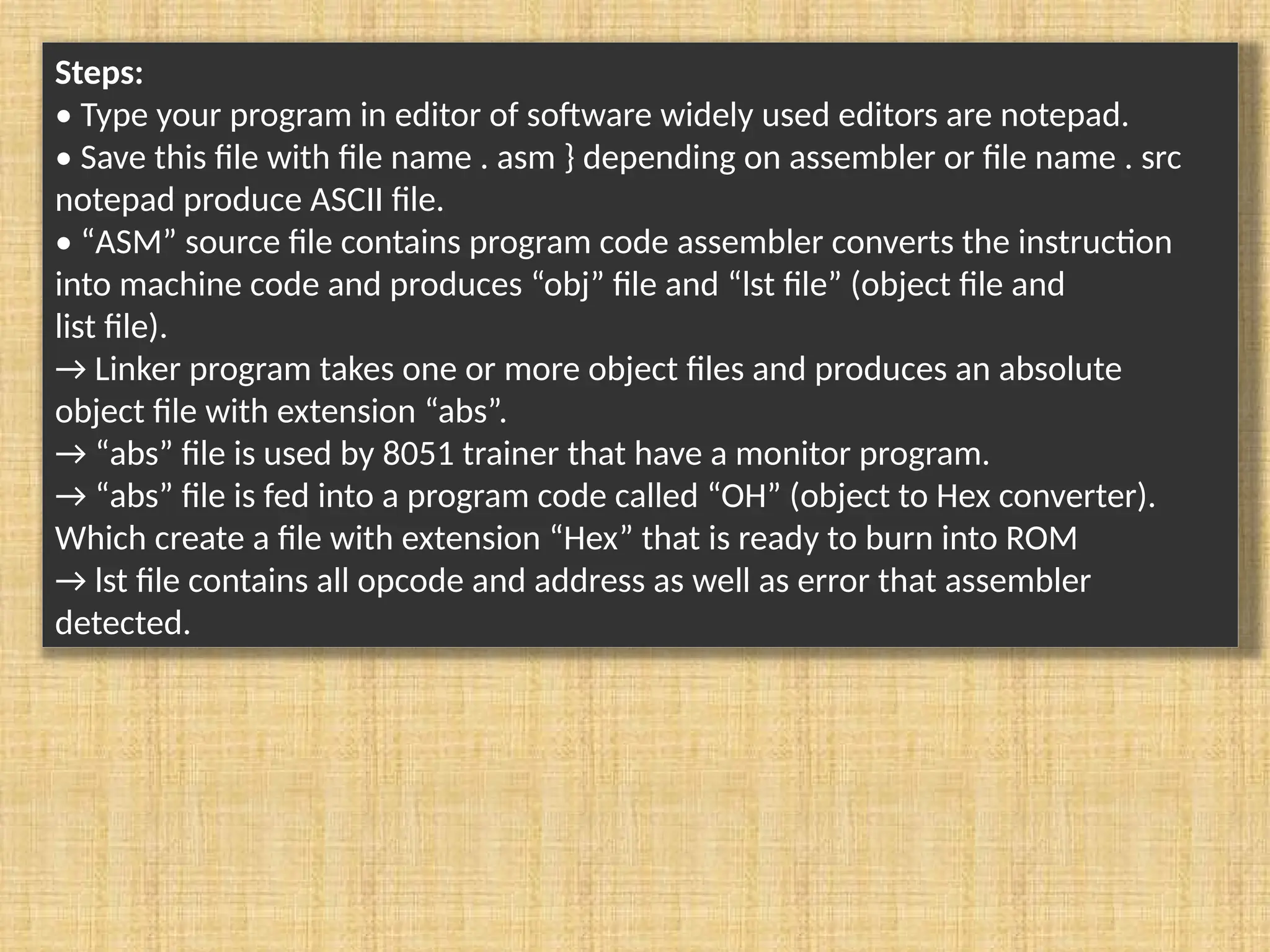
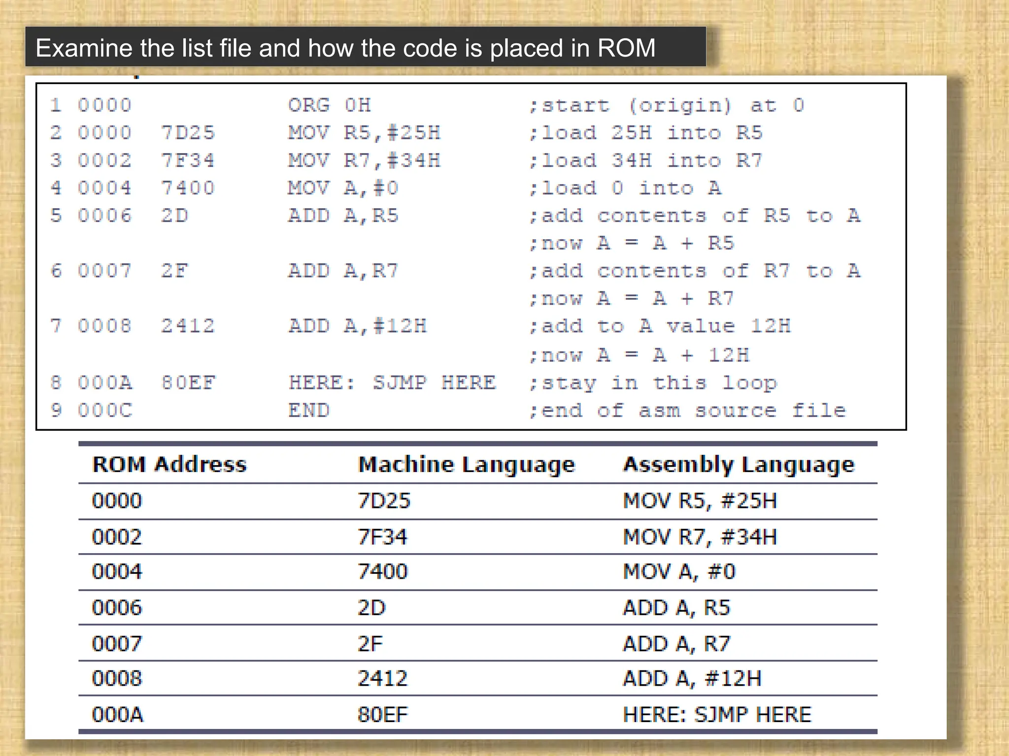
Steps: • Type yourprogram in editor of software widely used editors are notepad. • Save this file with file name . asm } depending on assembler or file name . src notepad produce ASCII file. • “ASM” source file contains program code assembler converts the instruction into machine code and produces “obj” file and “lst file” (object file and list file). → Linker program takes one or more object files and produces an absolute object file with extension “abs”. → “abs” file is used by 8051 trainer that have a monitor program. → “abs” file is fed into a program code called “OH” (object to Hex converter). Which create a file with extension “Hex” that is ready to burn into ROM → lst file contains all opcode and address as well as error that assembler detected.
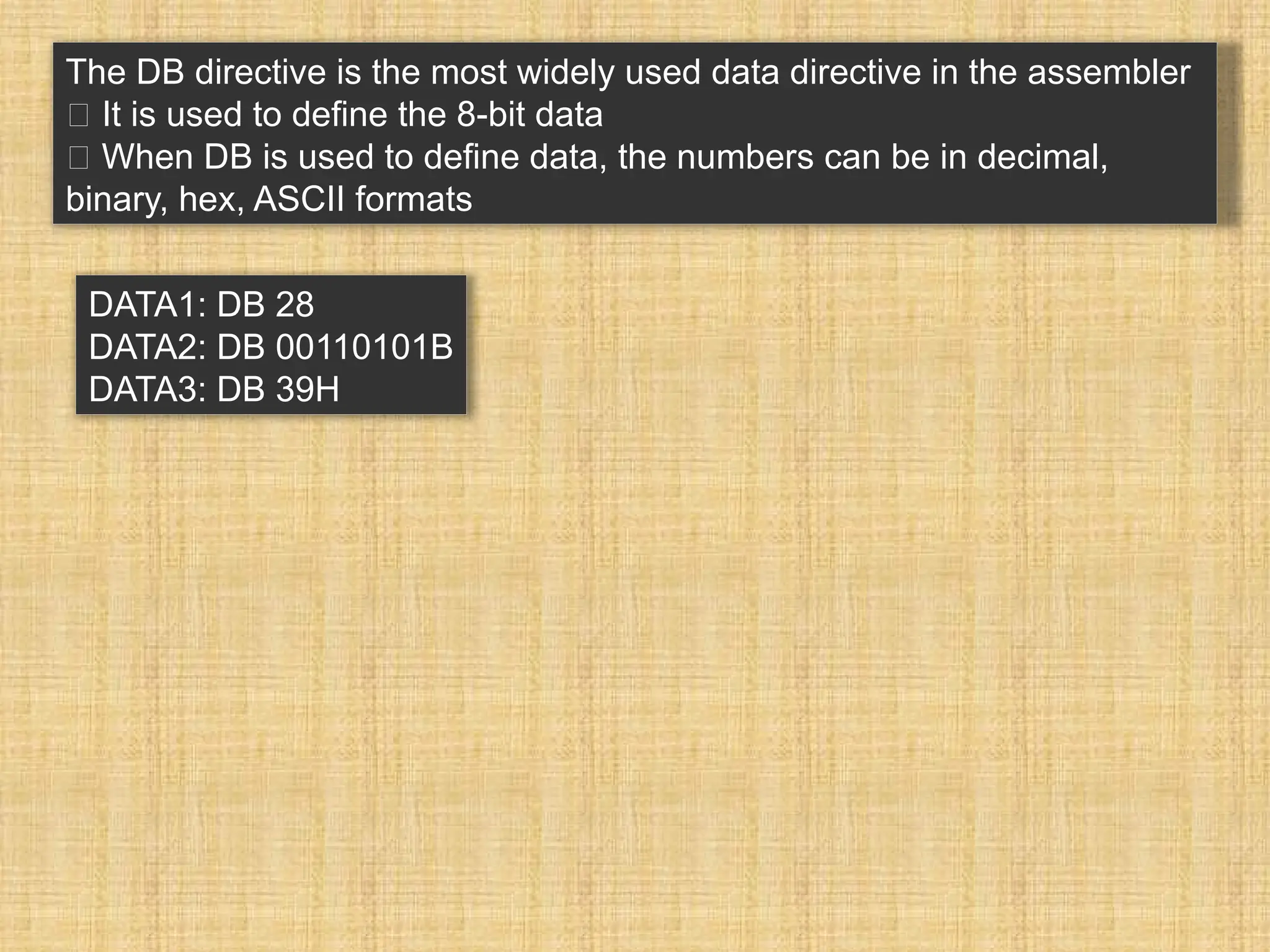
The DB directiveis the most widely used data directive in the assembler It is used to define the 8-bit data When DB is used to define data, the numbers can be in decimal, binary, hex, ASCII formats DATA1: DB 28 DATA2: DB 00110101B DATA3: DB 39H
49.
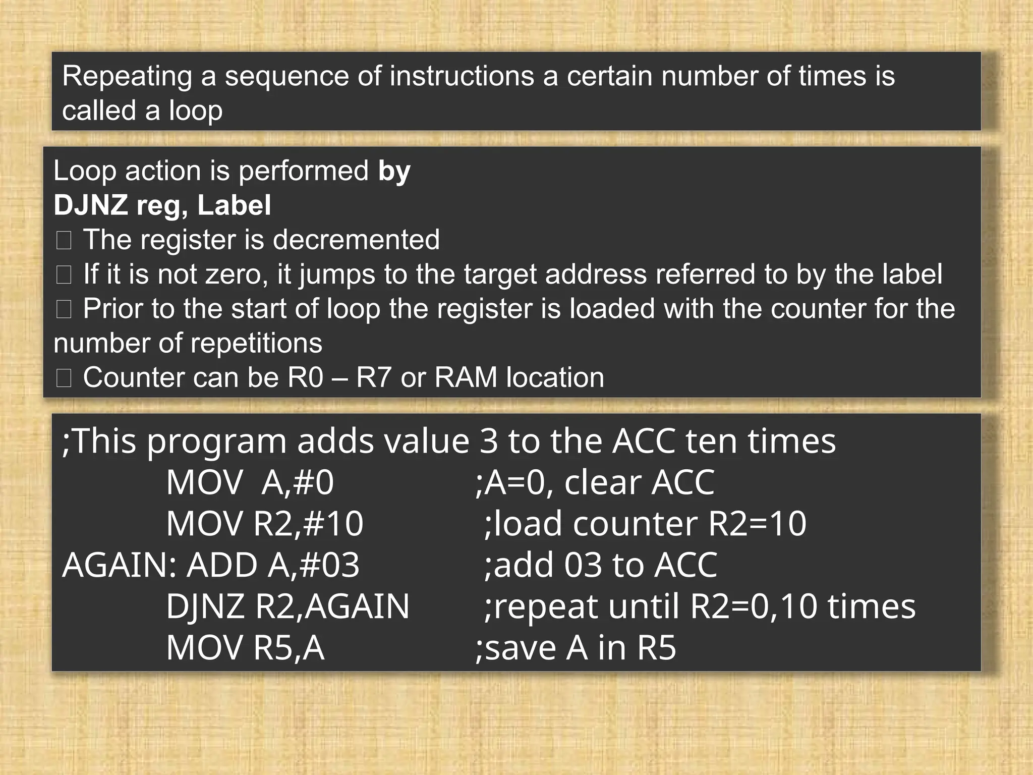
Repeating a sequenceof instructions a certain number of times is called a loop Loop action is performed by DJNZ reg, Label The register is decremented If it is not zero, it jumps to the target address referred to by the label Prior to the start of loop the register is loaded with the counter for the number of repetitions Counter can be R0 – R7 or RAM location ;This program adds value 3 to the ACC ten times MOV A,#0 ;A=0, clear ACC MOV R2,#10 ;load counter R2=10 AGAIN: ADD A,#03 ;add 03 to ACC DJNZ R2,AGAIN ;repeat until R2=0,10 times MOV R5,A ;save A in R5
50.
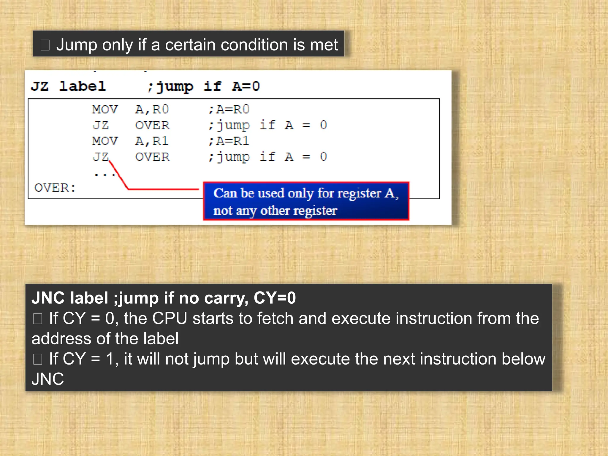
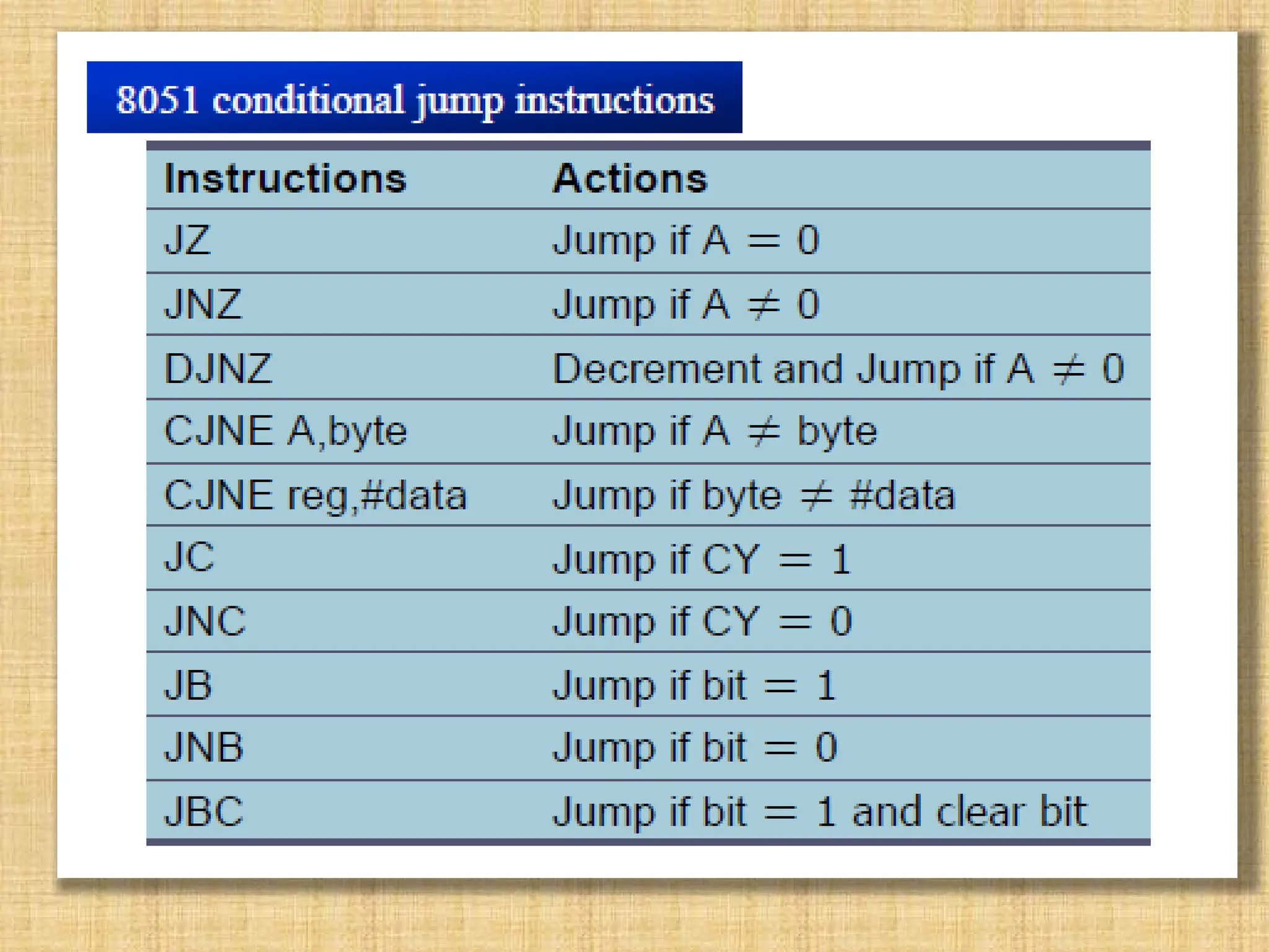
Jump onlyif a certain condition is met JNC label ;jump if no carry, CY=0 If CY = 0, the CPU starts to fetch and execute instruction from the address of the label If CY = 1, it will not jump but will execute the next instruction below JNC
52.
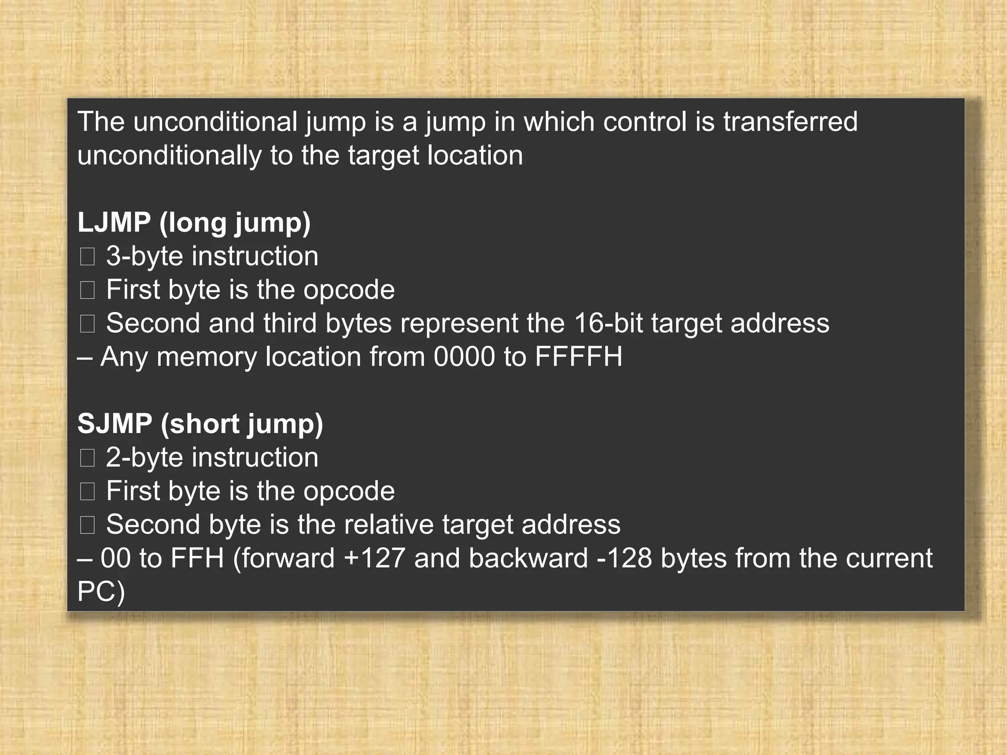
The unconditional jumpis a jump in which control is transferred unconditionally to the target location LJMP (long jump) 3-byte instruction First byte is the opcode Second and third bytes represent the 16-bit target address – Any memory location from 0000 to FFFFH SJMP (short jump) 2-byte instruction First byte is the opcode Second byte is the relative target address – 00 to FFH (forward +127 and backward -128 bytes from the current PC)
53.
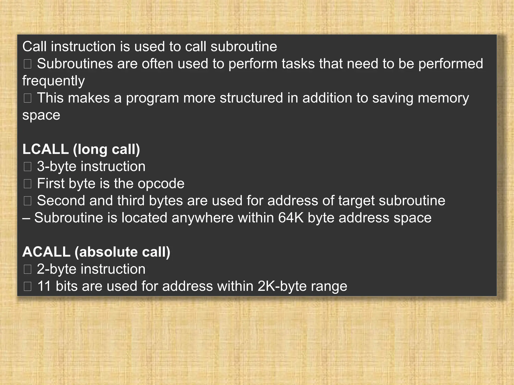
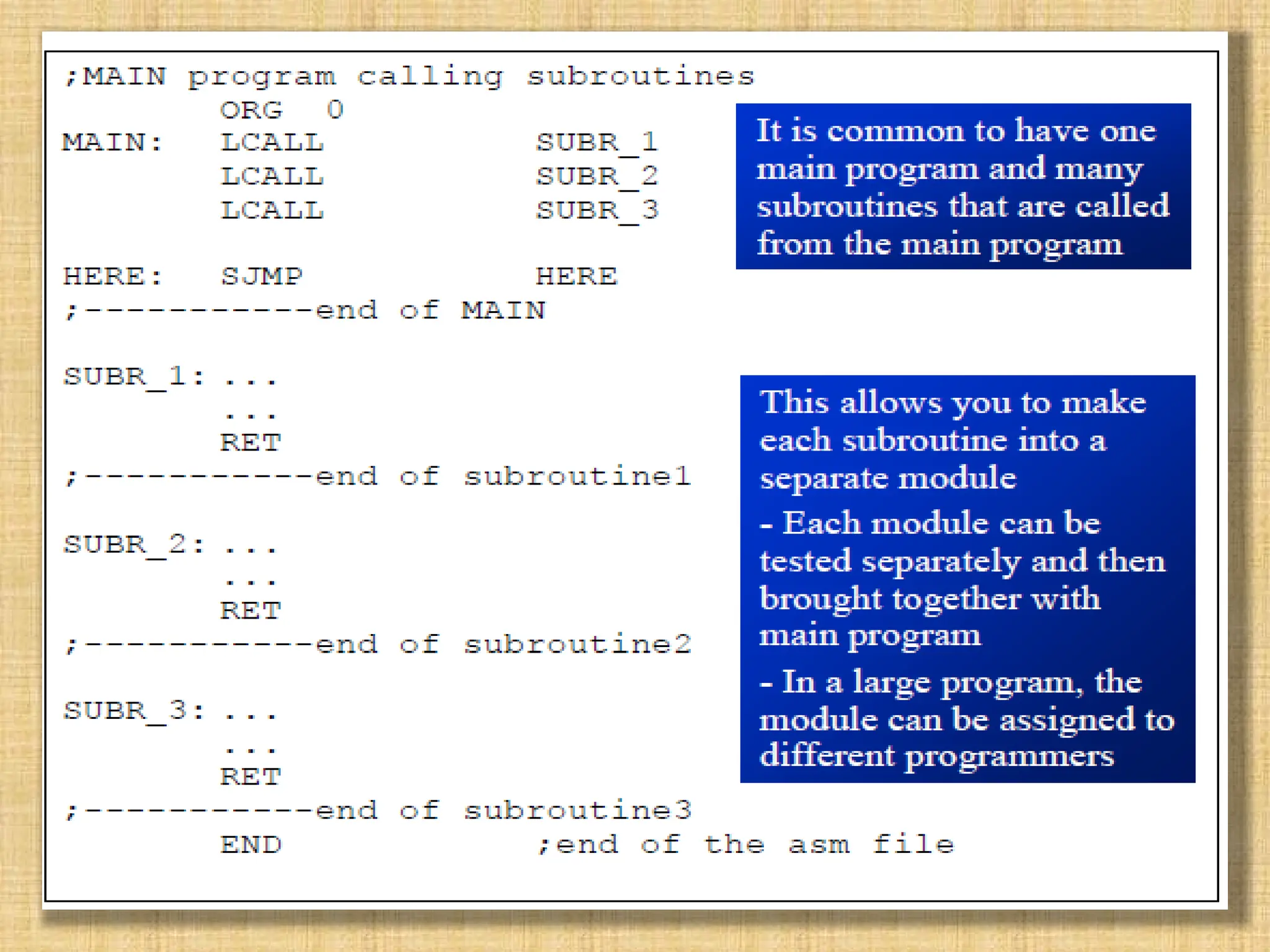
Call instruction isused to call subroutine Subroutines are often used to perform tasks that need to be performed frequently This makes a program more structured in addition to saving memory space LCALL (long call) 3-byte instruction First byte is the opcode Second and third bytes are used for address of target subroutine – Subroutine is located anywhere within 64K byte address space ACALL (absolute call) 2-byte instruction 11 bits are used for address within 2K-byte range
54.
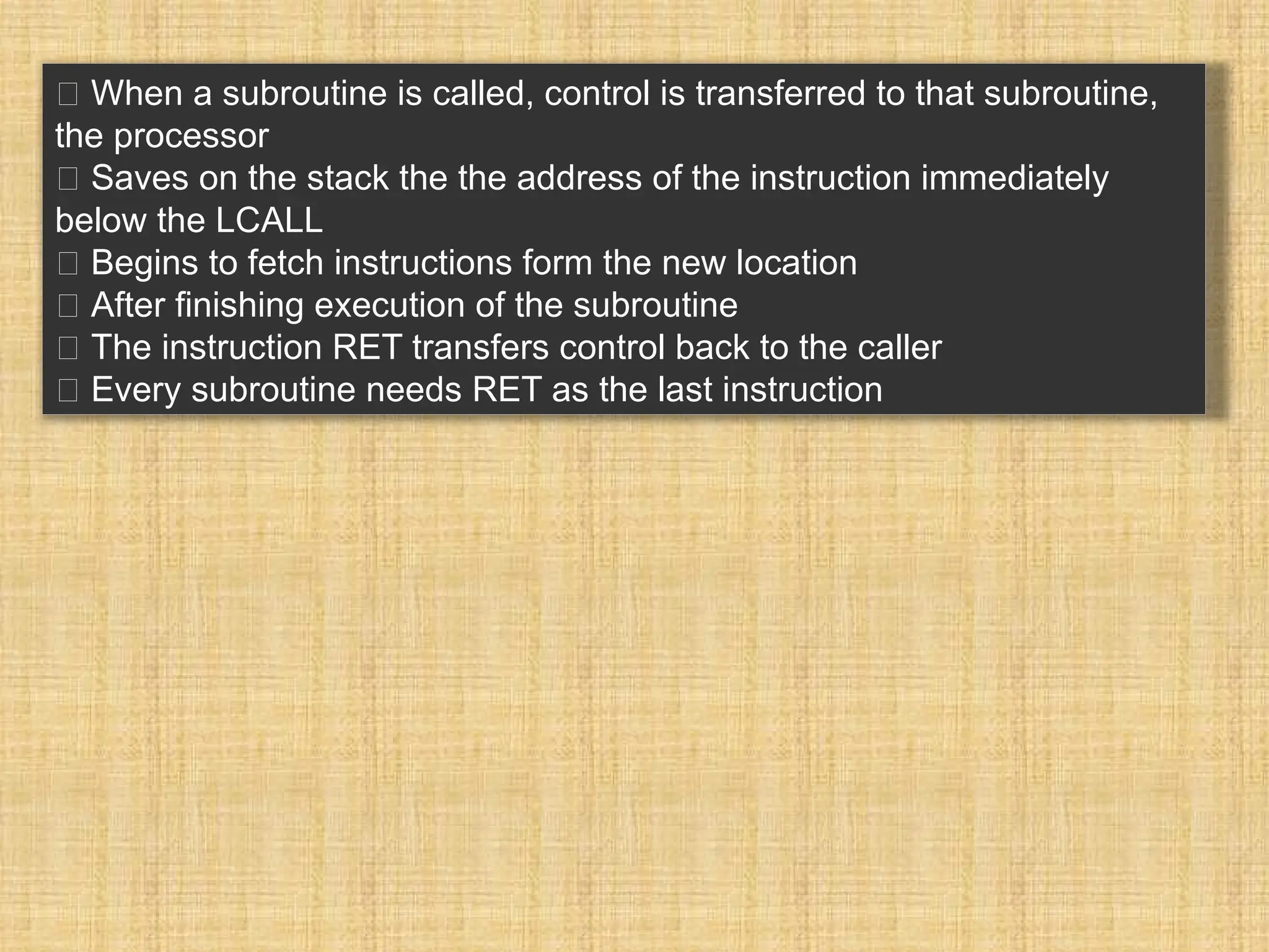
When asubroutine is called, control is transferred to that subroutine, the processor Saves on the stack the the address of the instruction immediately below the LCALL Begins to fetch instructions form the new location After finishing execution of the subroutine The instruction RET transfers control back to the caller Every subroutine needs RET as the last instruction
56.
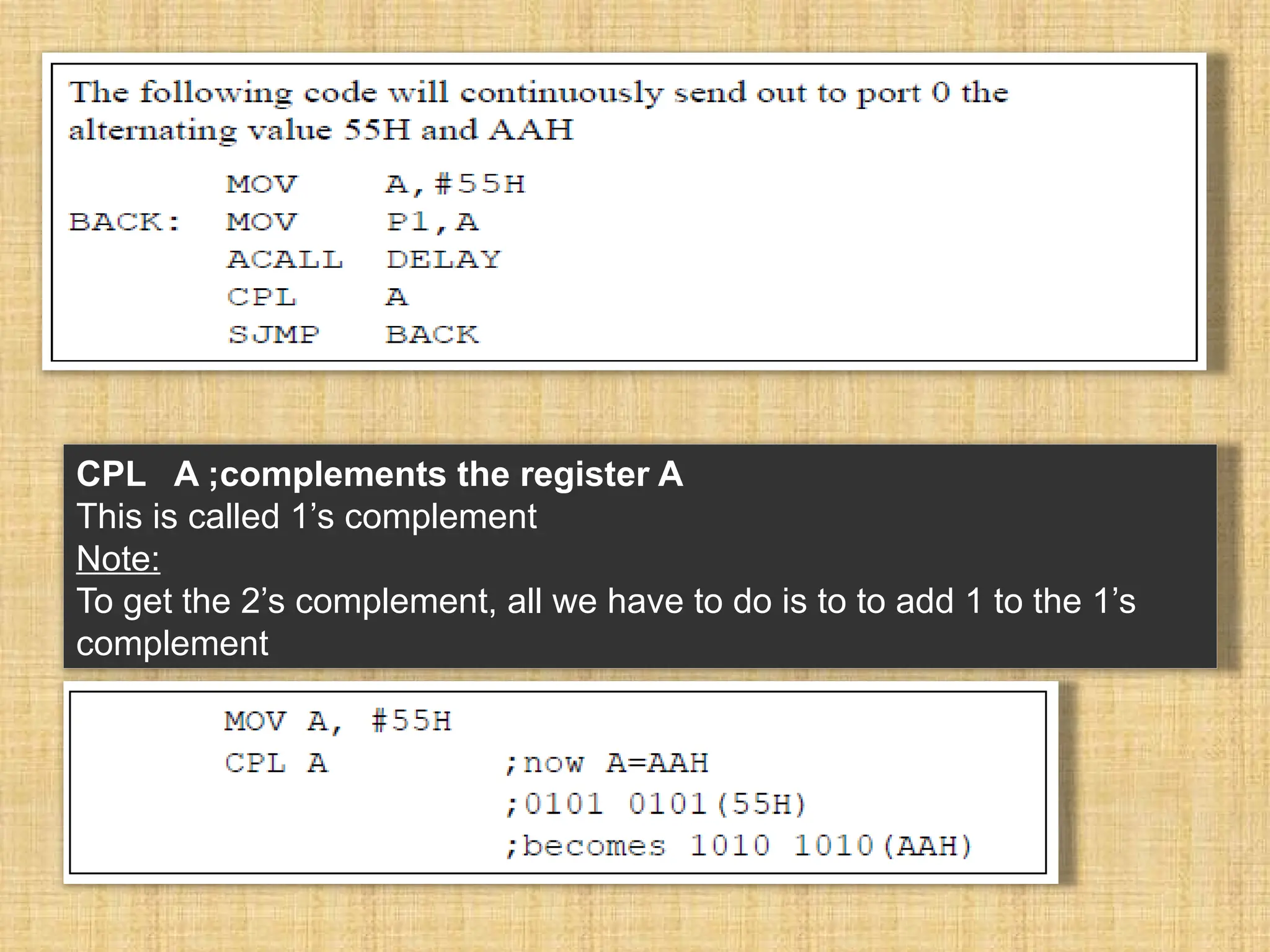
CPL A ;complementsthe register A This is called 1’s complement Note: To get the 2’s complement, all we have to do is to to add 1 to the 1’s complement
57.
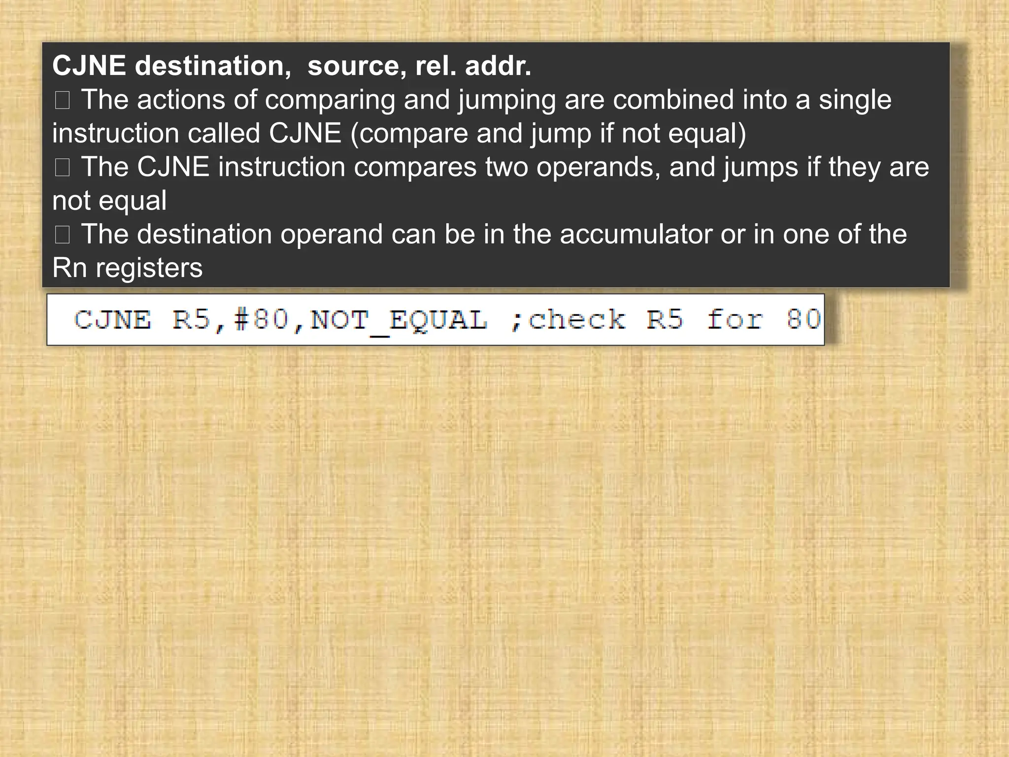
CJNE destination, source,rel. addr. The actions of comparing and jumping are combined into a single instruction called CJNE (compare and jump if not equal) The CJNE instruction compares two operands, and jumps if they are not equal The destination operand can be in the accumulator or in one of the Rn registers
58.
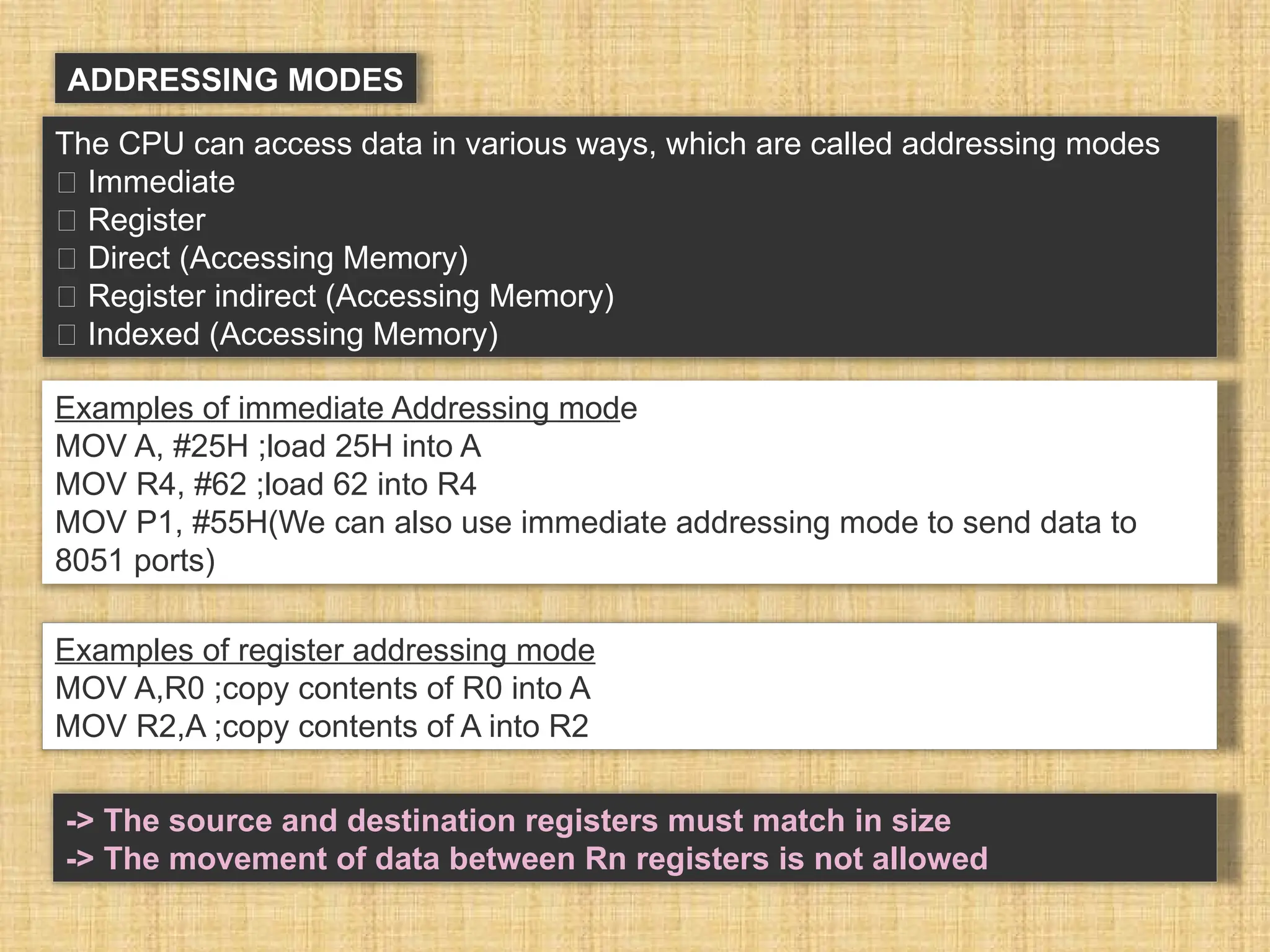
ADDRESSING MODES The CPUcan access data in various ways, which are called addressing modes Immediate Register Direct (Accessing Memory) Register indirect (Accessing Memory) Indexed (Accessing Memory) Examples of immediate Addressing mode MOV A, #25H ;load 25H into A MOV R4, #62 ;load 62 into R4 MOV P1, #55H(We can also use immediate addressing mode to send data to 8051 ports) Examples of register addressing mode MOV A,R0 ;copy contents of R0 into A MOV R2,A ;copy contents of A into R2 -> The source and destination registers must match in size -> The movement of data between Rn registers is not allowed
59.
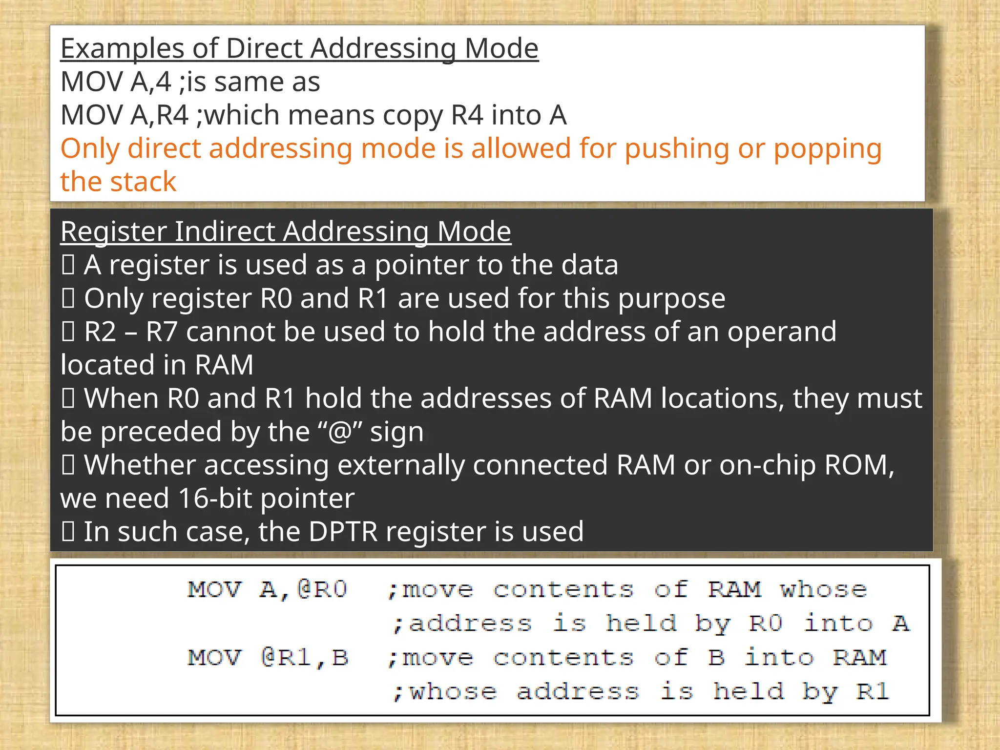
Examples of DirectAddressing Mode MOV A,4 ;is same as MOV A,R4 ;which means copy R4 into A Only direct addressing mode is allowed for pushing or popping the stack Register Indirect Addressing Mode A register is used as a pointer to the data Only register R0 and R1 are used for this purpose R2 – R7 cannot be used to hold the address of an operand located in RAM When R0 and R1 hold the addresses of RAM locations, they must be preceded by the “@” sign Whether accessing externally connected RAM or on-chip ROM, we need 16-bit pointer In such case, the DPTR register is used
60.
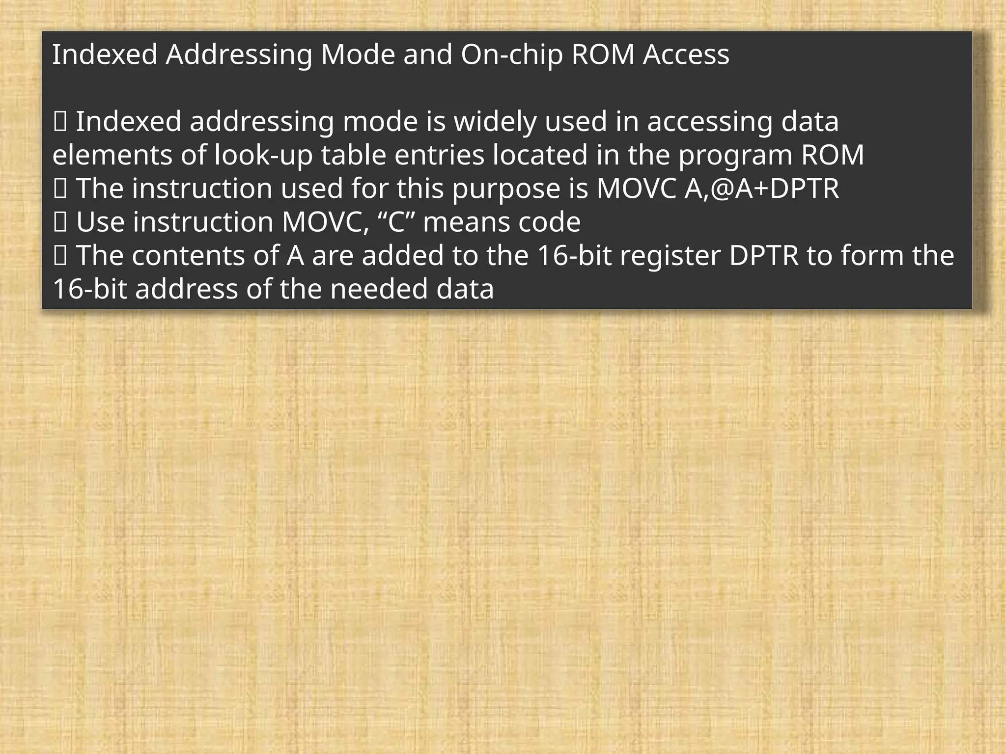
Indexed Addressing Modeand On-chip ROM Access Indexed addressing mode is widely used in accessing data elements of look-up table entries located in the program ROM The instruction used for this purpose is MOVC A,@A+DPTR Use instruction MOVC, “C” means code The contents of A are added to the 16-bit register DPTR to form the 16-bit address of the needed data
61.
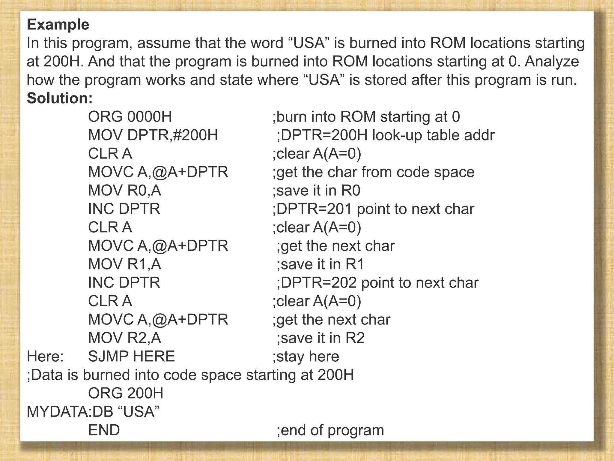
Example In this program,assume that the word “USA” is burned into ROM locations starting at 200H. And that the program is burned into ROM locations starting at 0. Analyze how the program works and state where “USA” is stored after this program is run. Solution: ORG 0000H ;burn into ROM starting at 0 MOV DPTR,#200H ;DPTR=200H look-up table addr CLR A ;clear A(A=0) MOVC A,@A+DPTR ;get the char from code space MOV R0,A ;save it in R0 INC DPTR ;DPTR=201 point to next char CLR A ;clear A(A=0) MOVC A,@A+DPTR ;get the next char MOV R1,A ;save it in R1 INC DPTR ;DPTR=202 point to next char CLR A ;clear A(A=0) MOVC A,@A+DPTR ;get the next char MOV R2,A ;save it in R2 Here: SJMP HERE ;stay here ;Data is burned into code space starting at 200H ORG 200H MYDATA:DB “USA” END ;end of program
62.
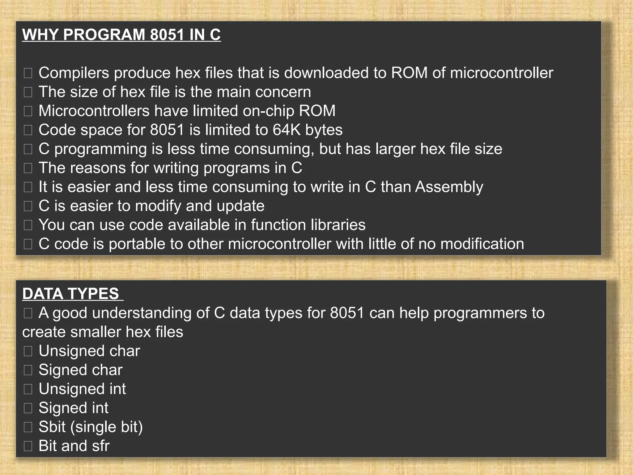
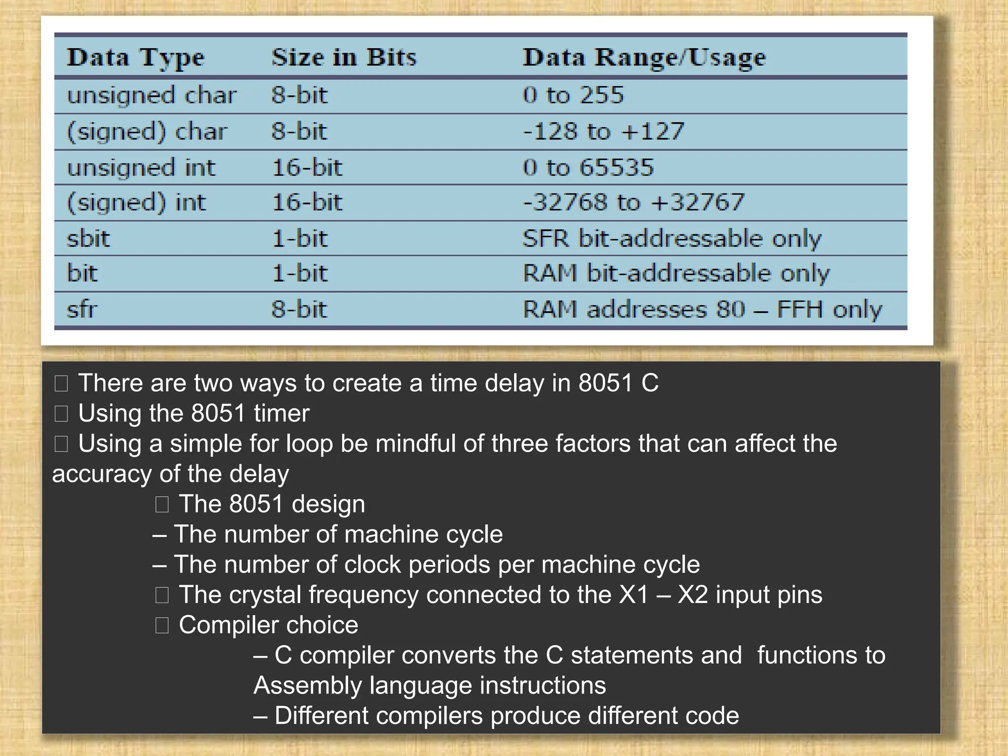
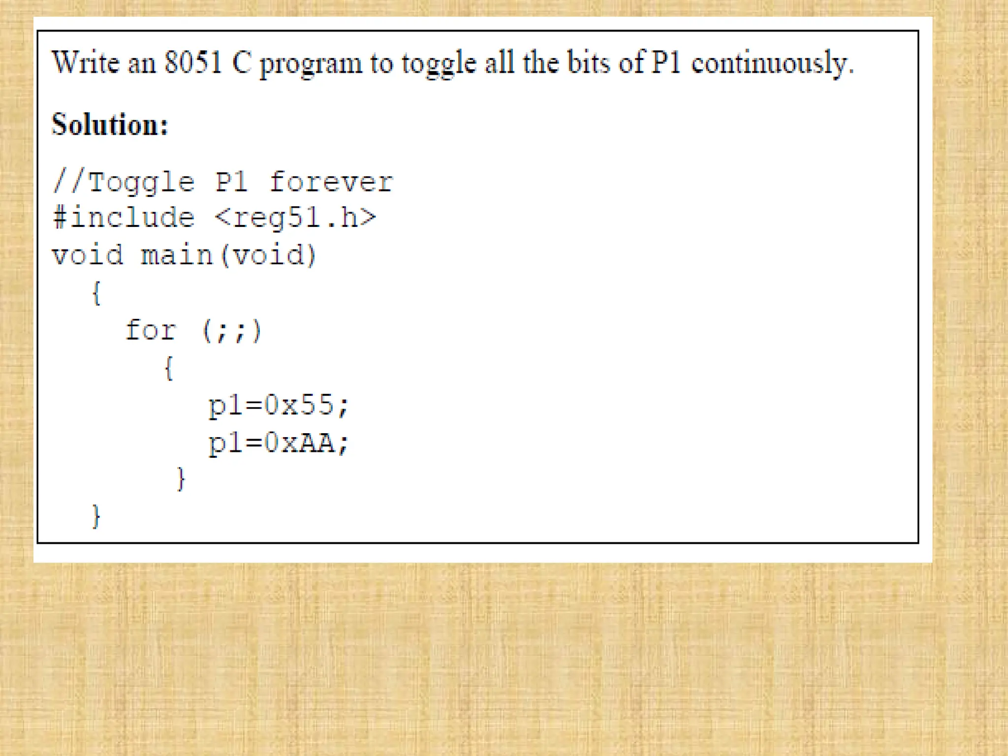
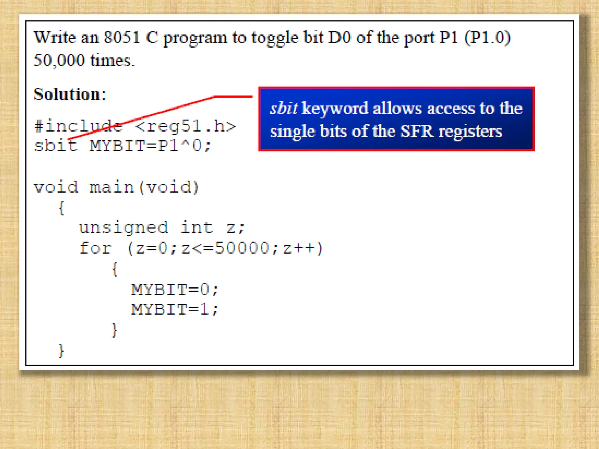
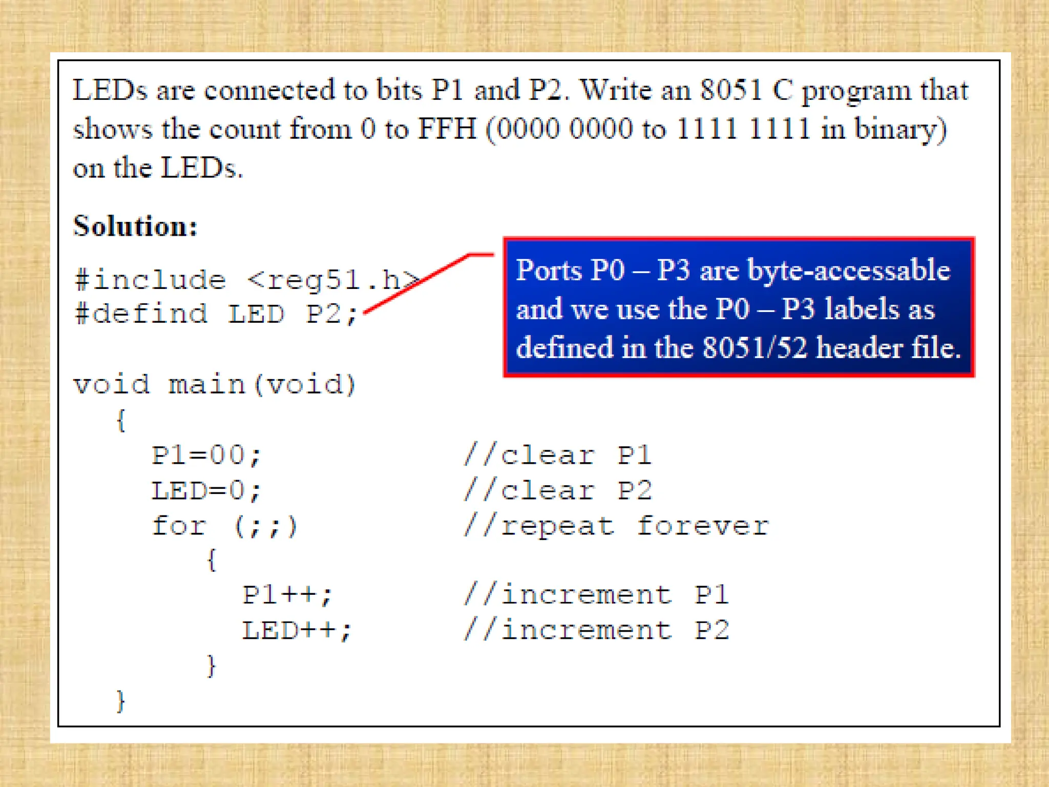
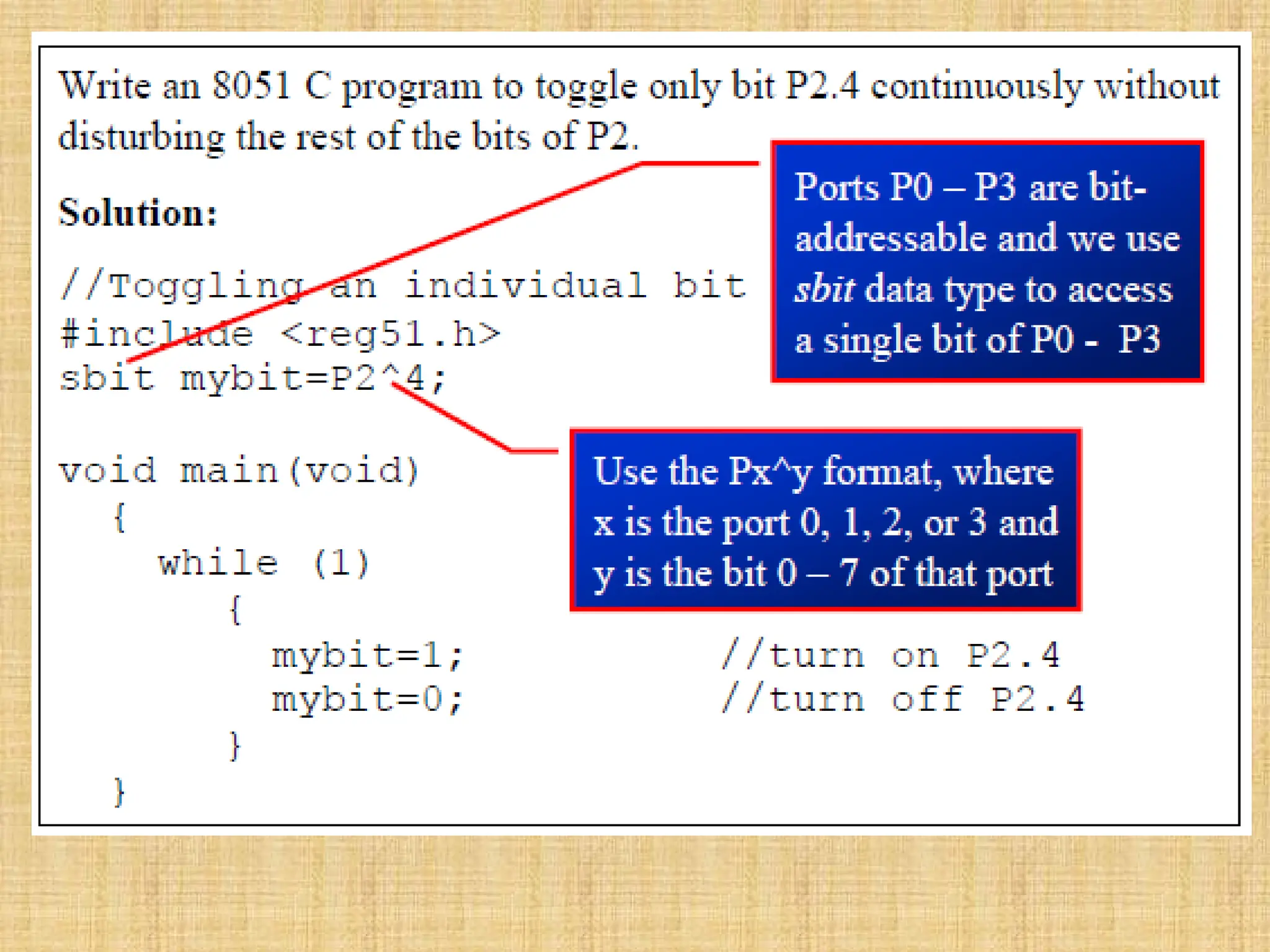
WHY PROGRAM 8051IN C Compilers produce hex files that is downloaded to ROM of microcontroller The size of hex file is the main concern Microcontrollers have limited on-chip ROM Code space for 8051 is limited to 64K bytes C programming is less time consuming, but has larger hex file size The reasons for writing programs in C It is easier and less time consuming to write in C than Assembly C is easier to modify and update You can use code available in function libraries C code is portable to other microcontroller with little of no modification DATA TYPES A good understanding of C data types for 8051 can help programmers to create smaller hex files Unsigned char Signed char Unsigned int Signed int Sbit (single bit) Bit and sfr
63.
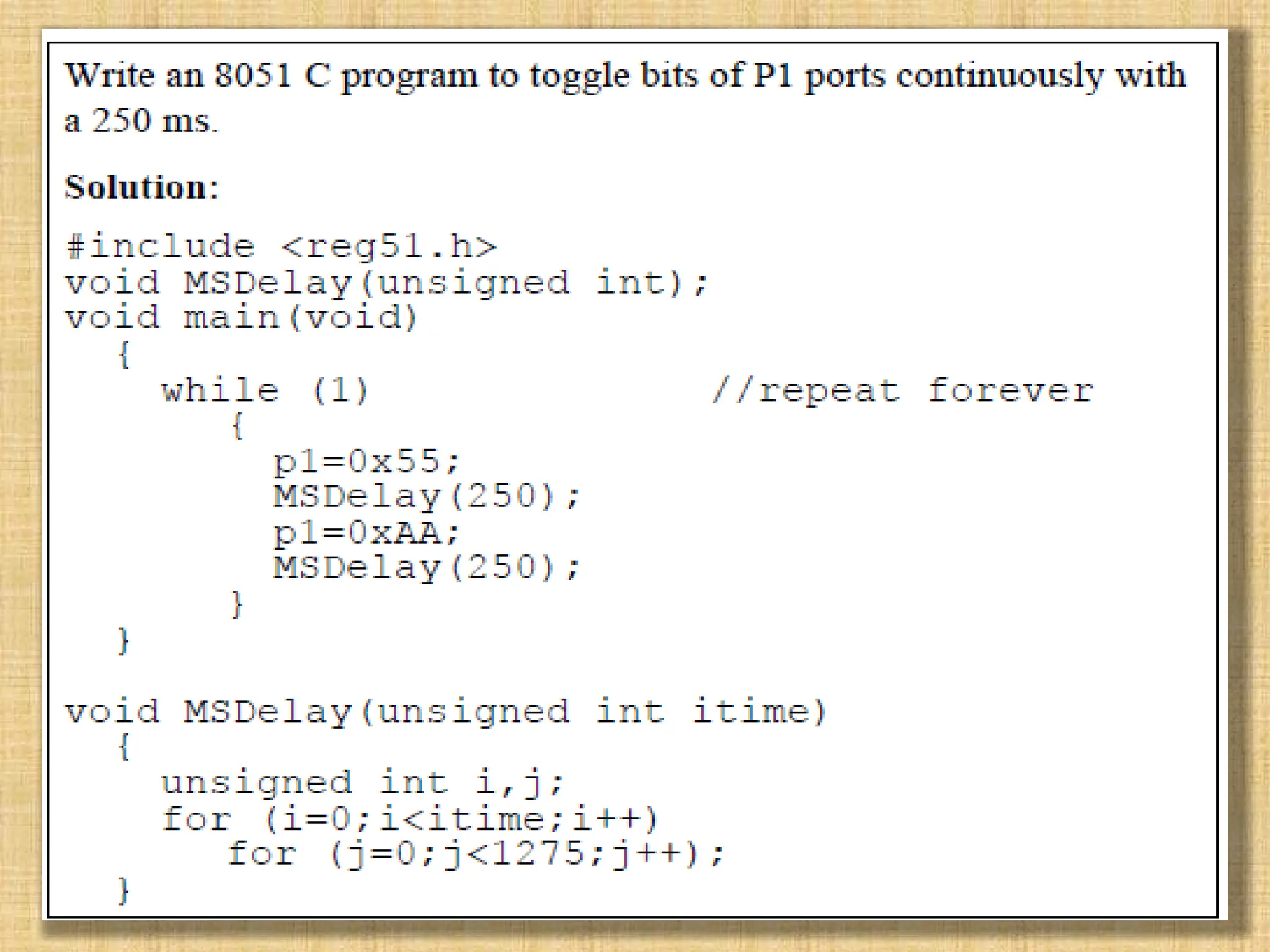
There aretwo ways to create a time delay in 8051 C Using the 8051 timer Using a simple for loop be mindful of three factors that can affect the accuracy of the delay The 8051 design – The number of machine cycle – The number of clock periods per machine cycle The crystal frequency connected to the X1 – X2 input pins Compiler choice – C compiler converts the C statements and functions to Assembly language instructions – Different compilers produce different code
64.
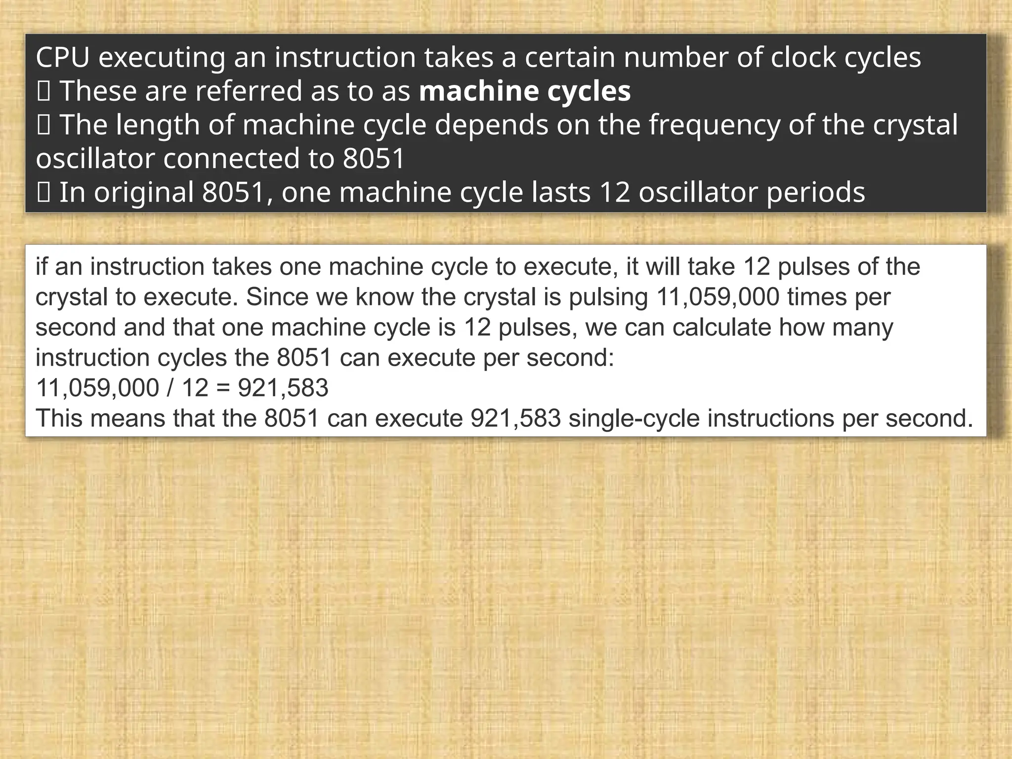
CPU executing aninstruction takes a certain number of clock cycles These are referred as to as machine cycles The length of machine cycle depends on the frequency of the crystal oscillator connected to 8051 In original 8051, one machine cycle lasts 12 oscillator periods if an instruction takes one machine cycle to execute, it will take 12 pulses of the crystal to execute. Since we know the crystal is pulsing 11,059,000 times per second and that one machine cycle is 12 pulses, we can calculate how many instruction cycles the 8051 can execute per second: 11,059,000 / 12 = 921,583 This means that the 8051 can execute 921,583 single-cycle instructions per second.
68.
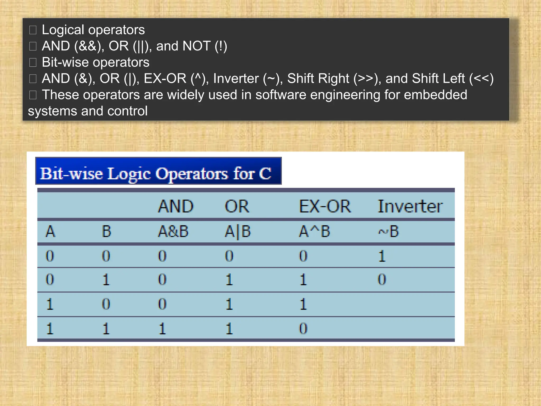
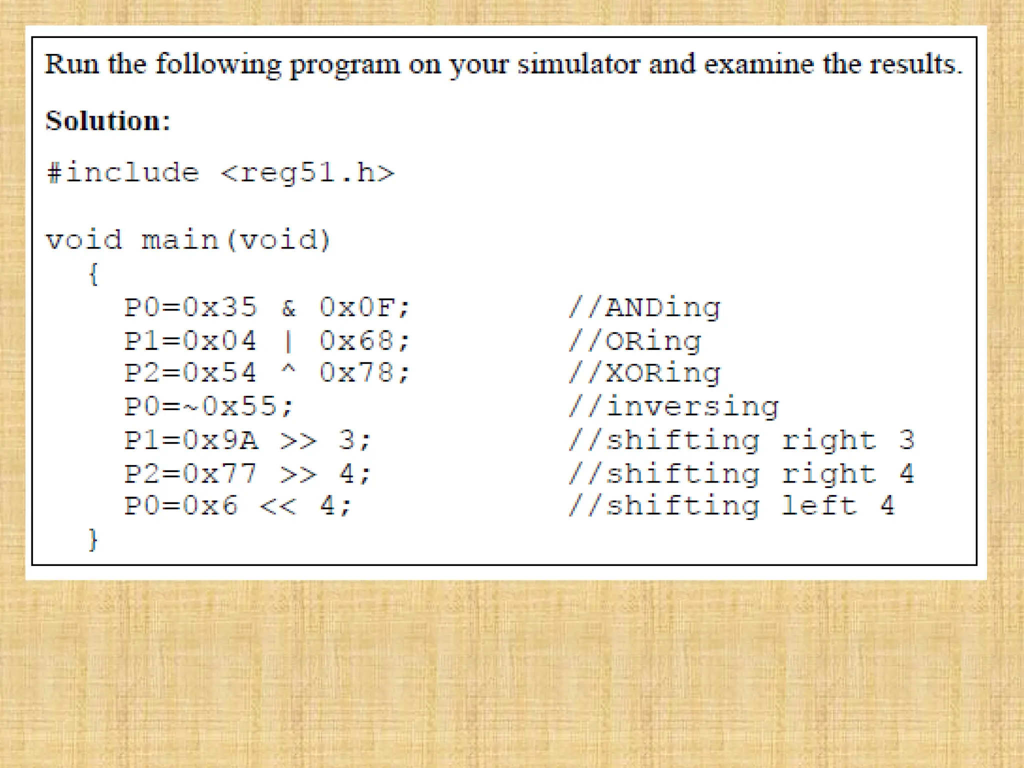
Logical operators AND (&&), OR (||), and NOT (!) Bit-wise operators AND (&), OR (|), EX-OR (^), Inverter (~), Shift Right (>>), and Shift Left (<<) These operators are widely used in software engineering for embedded systems and control
74.
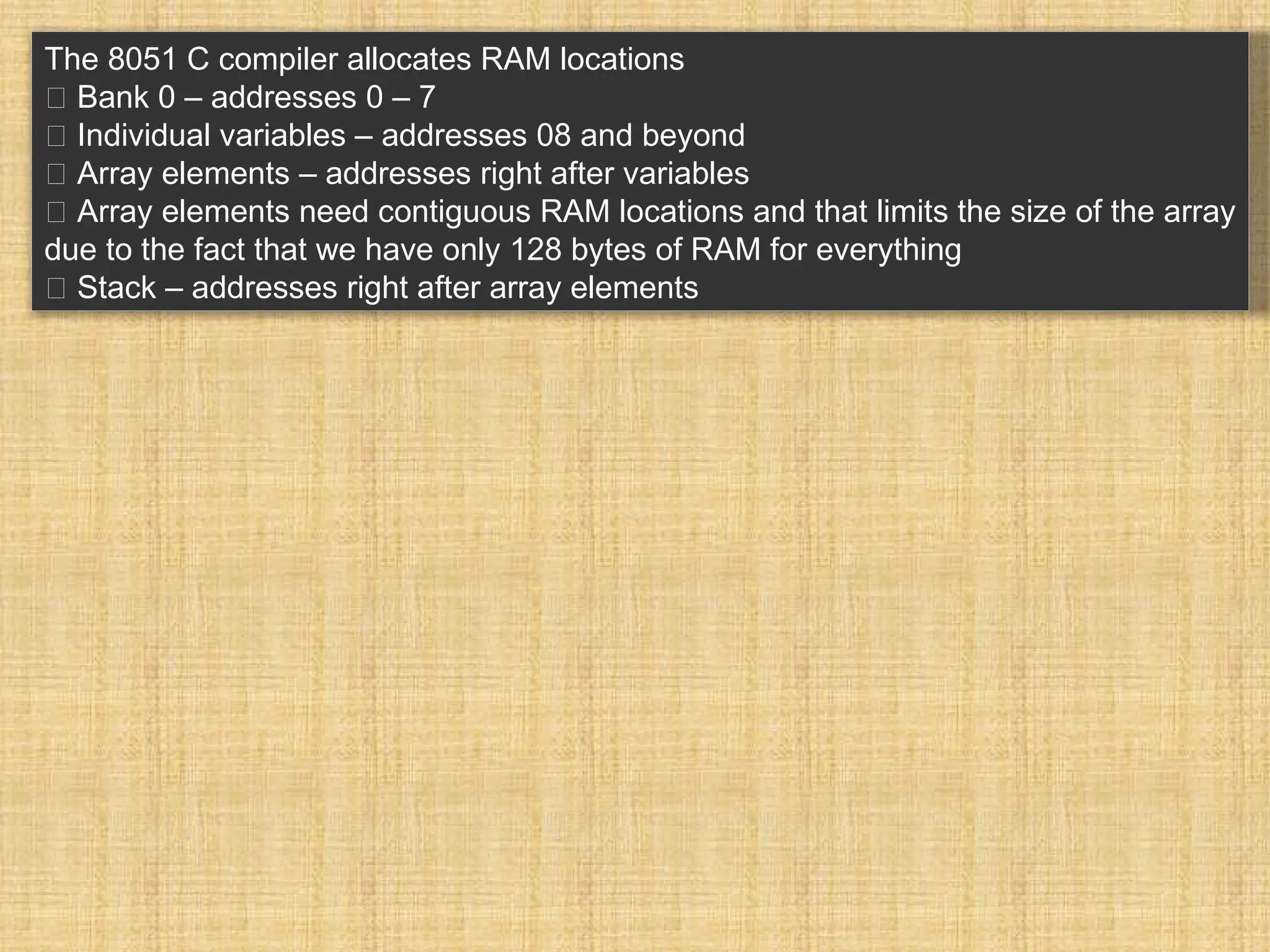
The 8051 Ccompiler allocates RAM locations Bank 0 – addresses 0 – 7 Individual variables – addresses 08 and beyond Array elements – addresses right after variables Array elements need contiguous RAM locations and that limits the size of the array due to the fact that we have only 128 bytes of RAM for everything Stack – addresses right after array elements
75.
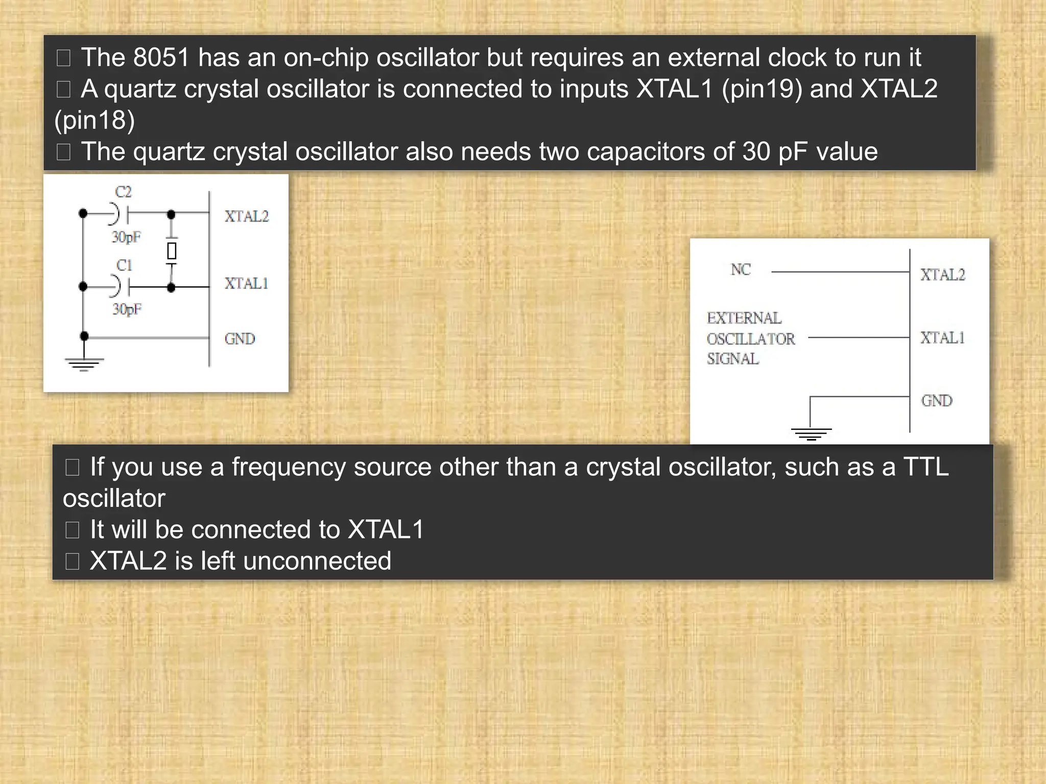
The 8051has an on-chip oscillator but requires an external clock to run it A quartz crystal oscillator is connected to inputs XTAL1 (pin19) and XTAL2 (pin18) The quartz crystal oscillator also needs two capacitors of 30 pF value If you use a frequency source other than a crystal oscillator, such as a TTL oscillator It will be connected to XTAL1 XTAL2 is left unconnected
76.
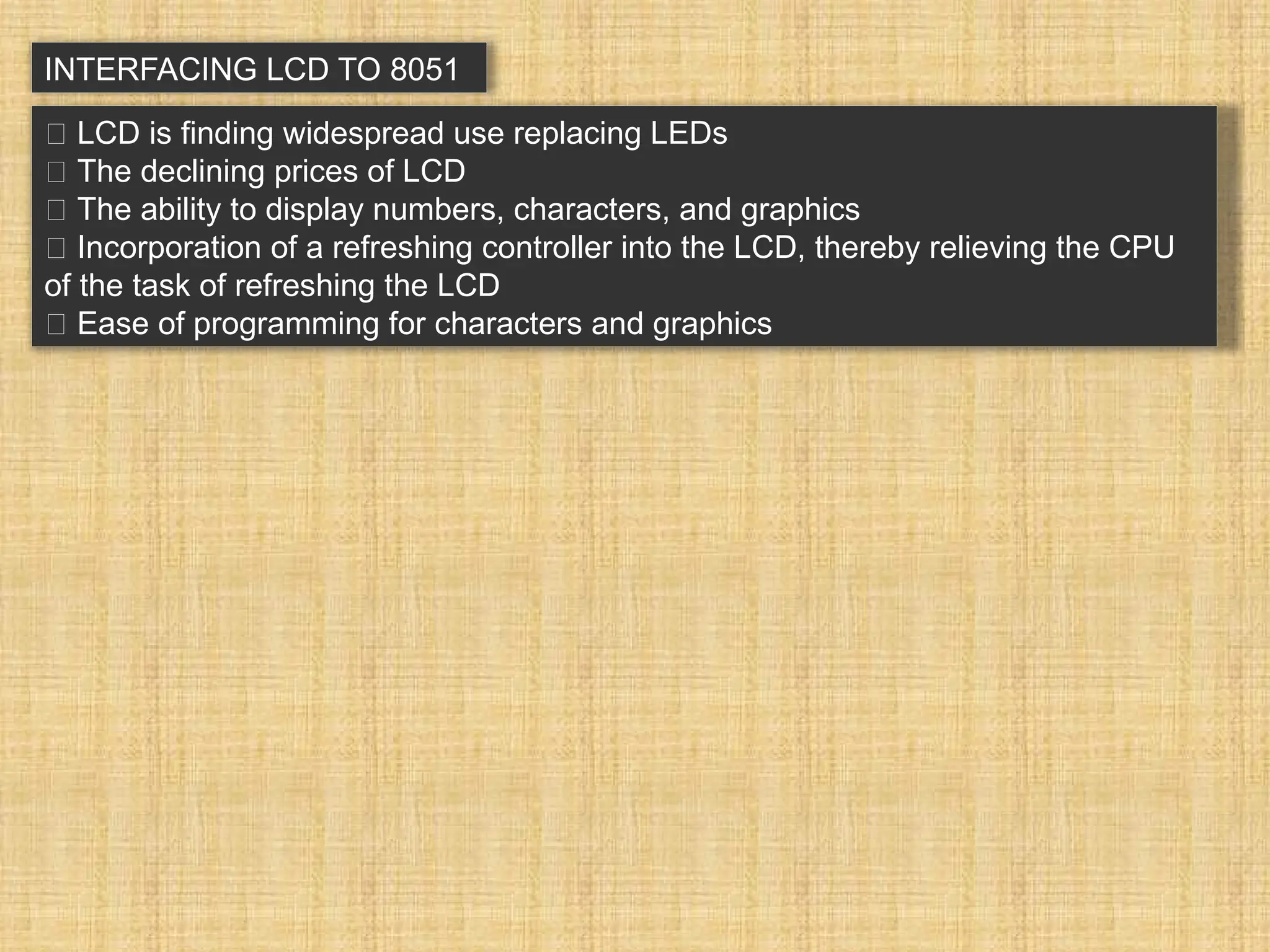
INTERFACING LCD TO8051 LCD is finding widespread use replacing LEDs The declining prices of LCD The ability to display numbers, characters, and graphics Incorporation of a refreshing controller into the LCD, thereby relieving the CPU of the task of refreshing the LCD Ease of programming for characters and graphics
78.
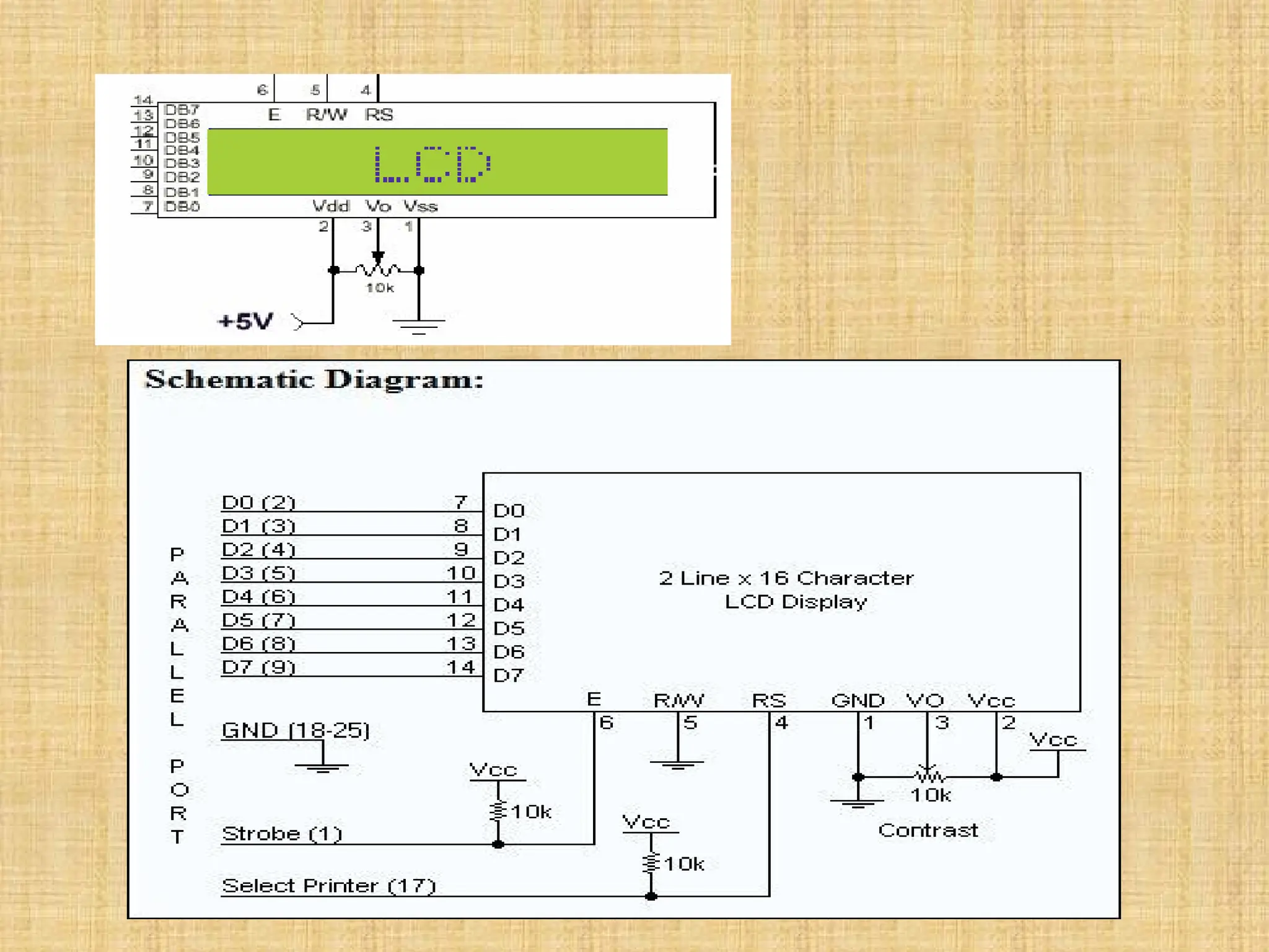
Above is thequite simple schematic. The LCD panel's Enable and Register Select is connected to the Control Port. The Control Port is an open collector / open drain output. While most Parallel Ports have internal pull-up resistors, there are a few which don't. Therefore by incorporating the two 10K external pull up resistors, the circuit is more portable for a wider range of computers, some of which may have no internal pull up resistors. We make no effort to place the Data bus into reverse direction. Therefore we hard wire the R/W line of the LCD panel, into write mode. This will cause no bus conflicts on the data lines. As a result we cannot read back the LCD's internal Busy Flag which tells us if the LCD has accepted and finished processing the last instruction. This problem is overcome by inserting known delays into our program. The 10k Potentiometer controls the contrast of the LCD panel. Nothing fancy here. As with all the examples, I've left the power supply out. You can use a bench power supply set to 5v or use a onboard +5 regulator. Remember a few de-coupling capacitors, especially if you have trouble with the circuit working properly.
79.
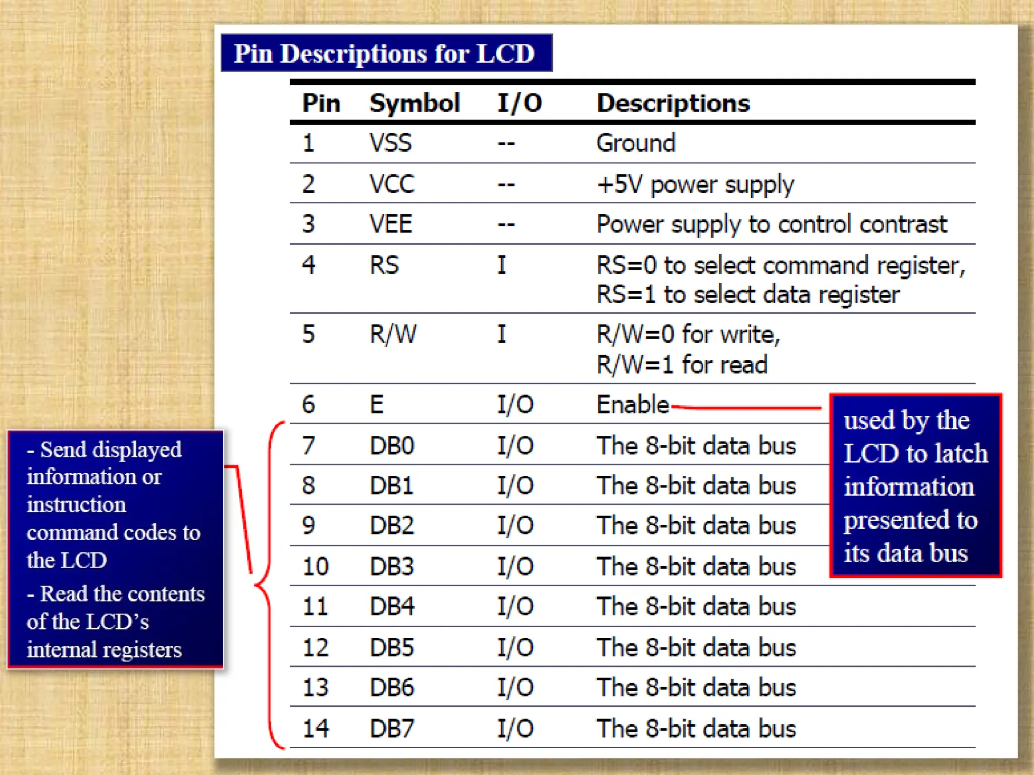
The 2line x 16 character LCD modules are available from a wide range of manufacturers and should all be compatible with the HD44780. The one I used to test this circuit was a Power tip PC- 1602F and an old Philips LTN211F-10 which was extracted from a Poker Machine! The diagram to the right, shows the pin numbers for these devices. When viewed from the front, the left pin is pin 14 and the right pin is pin 1. Logic status on control lines: • E - 0 Access to LCD disabled - 1 Access to LCD enabled • R/W - 0 Writing data to LCD - 1 Reading data from LCD • RS - 0 Instructions •1 Character
![An Assembly language instruction consists of four fields: [label:] Mnemonic [operands] [;comment]](https://image.slidesharecdn.com/8051-250217172308-ff9dd8f2/75/Microcontroller-8051-features-and-applications-35-2048.jpg)