Downloaded 193 times
![2 Programming technology for FPGAs The logic cells within an FPGA are configured using a programming technology. There are two classes of programming technology : [i] OTP(One time programmable) [ii] Reprogrammable Different FPGAs use different programmable (switching) elements : [i] Antifuse in ACTEL FPGA [ii] Static RAM cell in Xilinx FPGA [iii] EPROM/ EEPROM in Altera CPLD Programmable interconnect (PI) is used to connect any two logic cells. Different FPGAs use different interconnect architectures [i] Segmented Channel routing in ACTEL FPGA [ii] LCA interconnect architecture in Xilinx FPGA](https://image.slidesharecdn.com/ddhdlfpgaprogrammingtechinterconnect-140528084058-phpapp01/75/fpga-programming-2-2048.jpg)

![4 Programming technology for ACTEL FPGAs Actel’s Antifuse Two types of antifuses are used : [i] Poly-diffusion antifuse (Actel) [ii] Metal-metal antifuse (Quick Logic) Actel calls its antifuse as Programmable Low Impedance Circuit Element (PLICE) Advantage: small area overhead (size of the antifuse switching element is very small in comparison with size of sRAM cell) Disadvantage : OTP](https://image.slidesharecdn.com/ddhdlfpgaprogrammingtechinterconnect-140528084058-phpapp01/75/fpga-programming-4-2048.jpg)


This document discusses the programming technologies and interconnect architectures used in different FPGA devices. It covers antifuse-based OTP technologies used in Actel FPGAs, SRAM-based reprogrammable technologies used in Xilinx FPGAs, and EPROM/EEPROM technologies used in Altera CPLDs. It also describes the segmented channel routing interconnect architecture used in Actel FPGAs and the LCA architecture used in Xilinx FPGAs.
Introduction to FPGA programming technology and interconnect architecture by Dr. D.V. Kamath.
Details on OTP and reprogrammable technologies for FPGAs. Mention of antifuse, SRAM, and EEPROM.
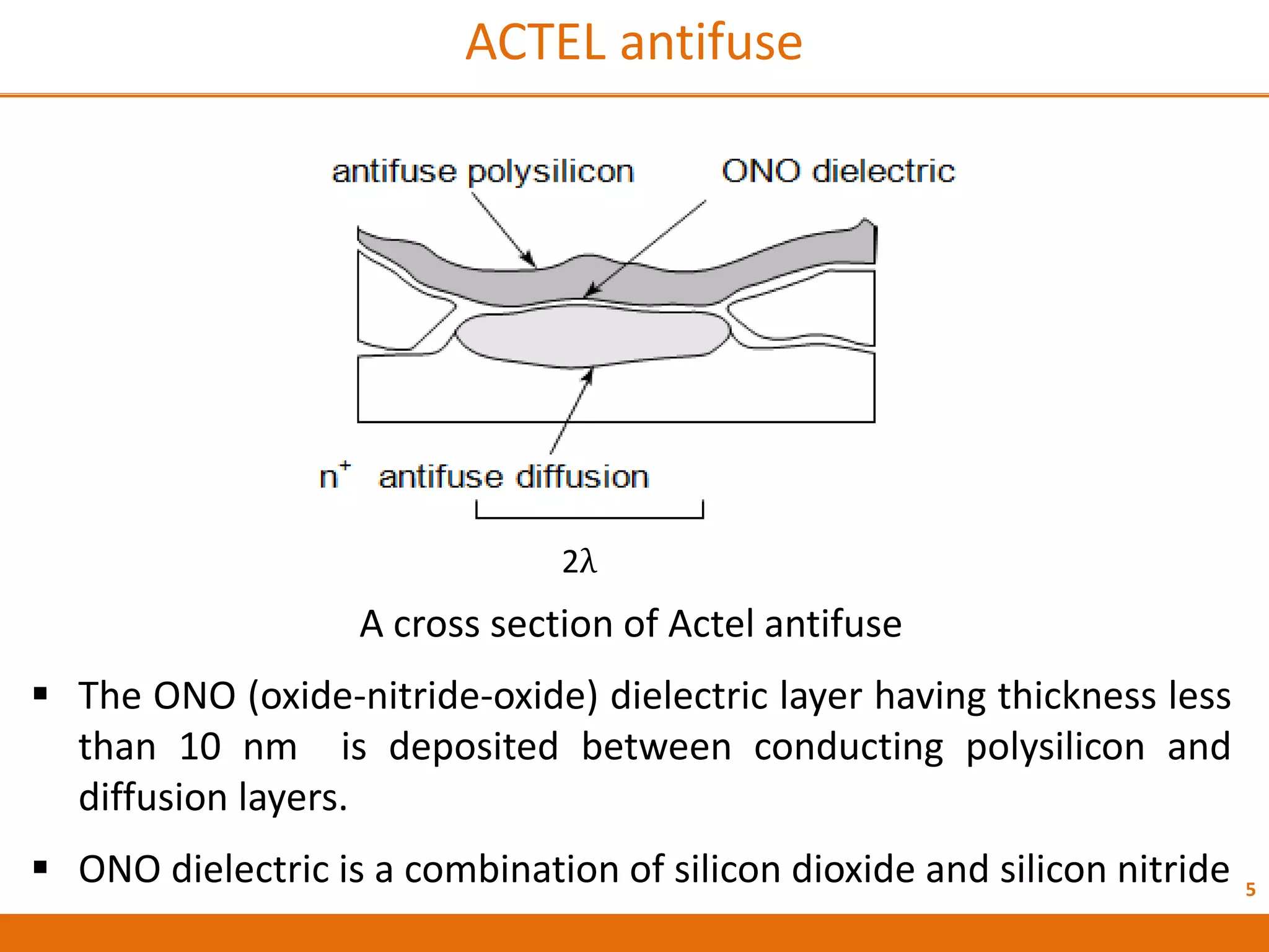
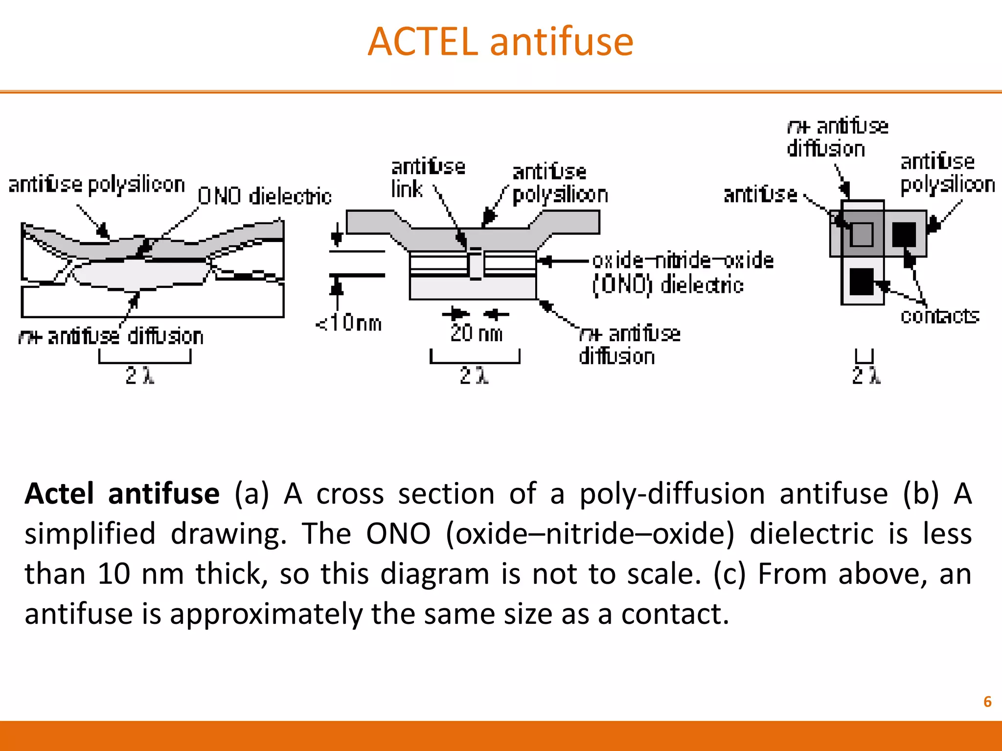
Explanation of antifuse technology for ACTEL FPGAs, including its structure and programming method.
Technical specifics of the ACTEL antifuse structure and its programming current impact.
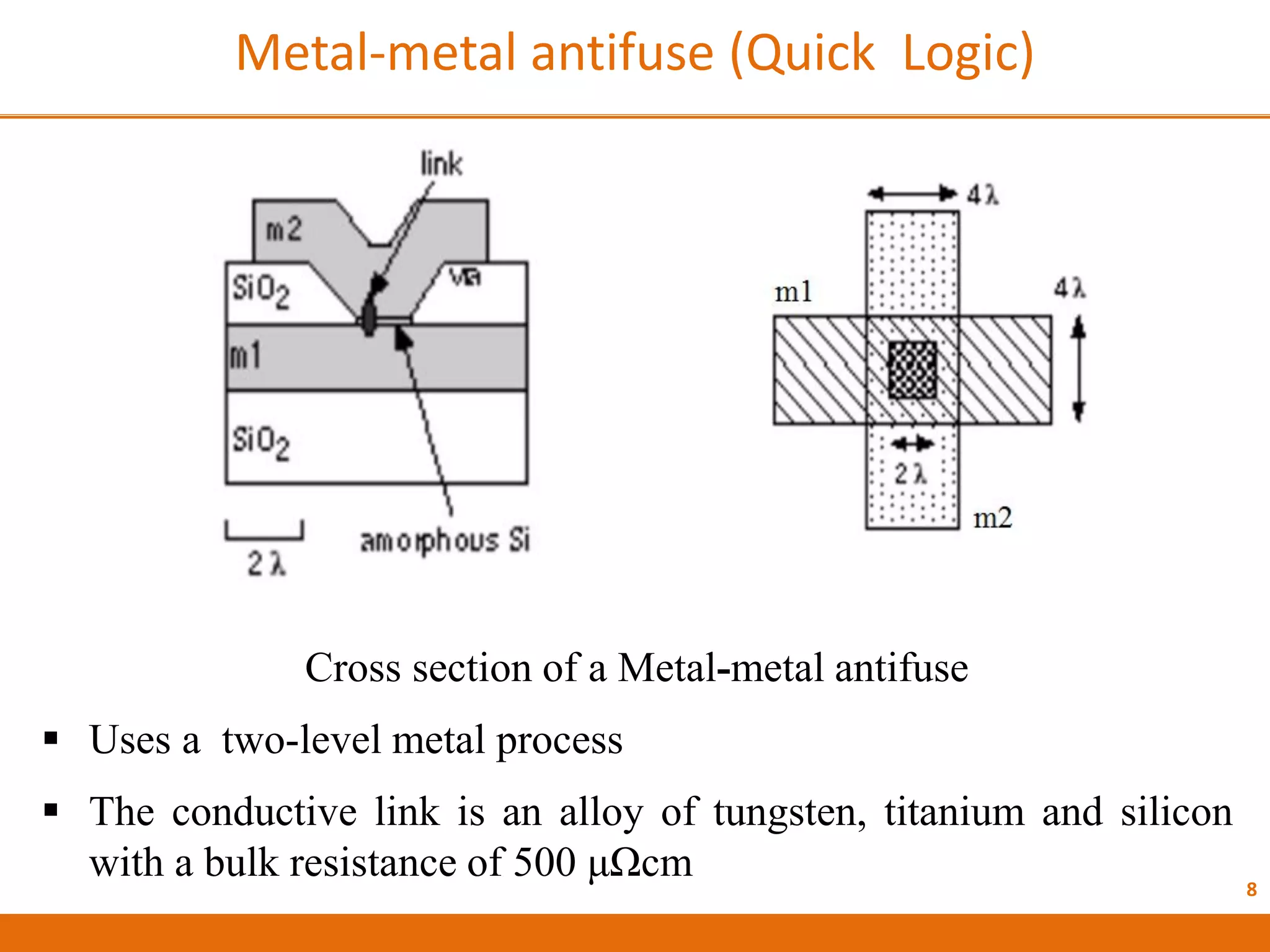
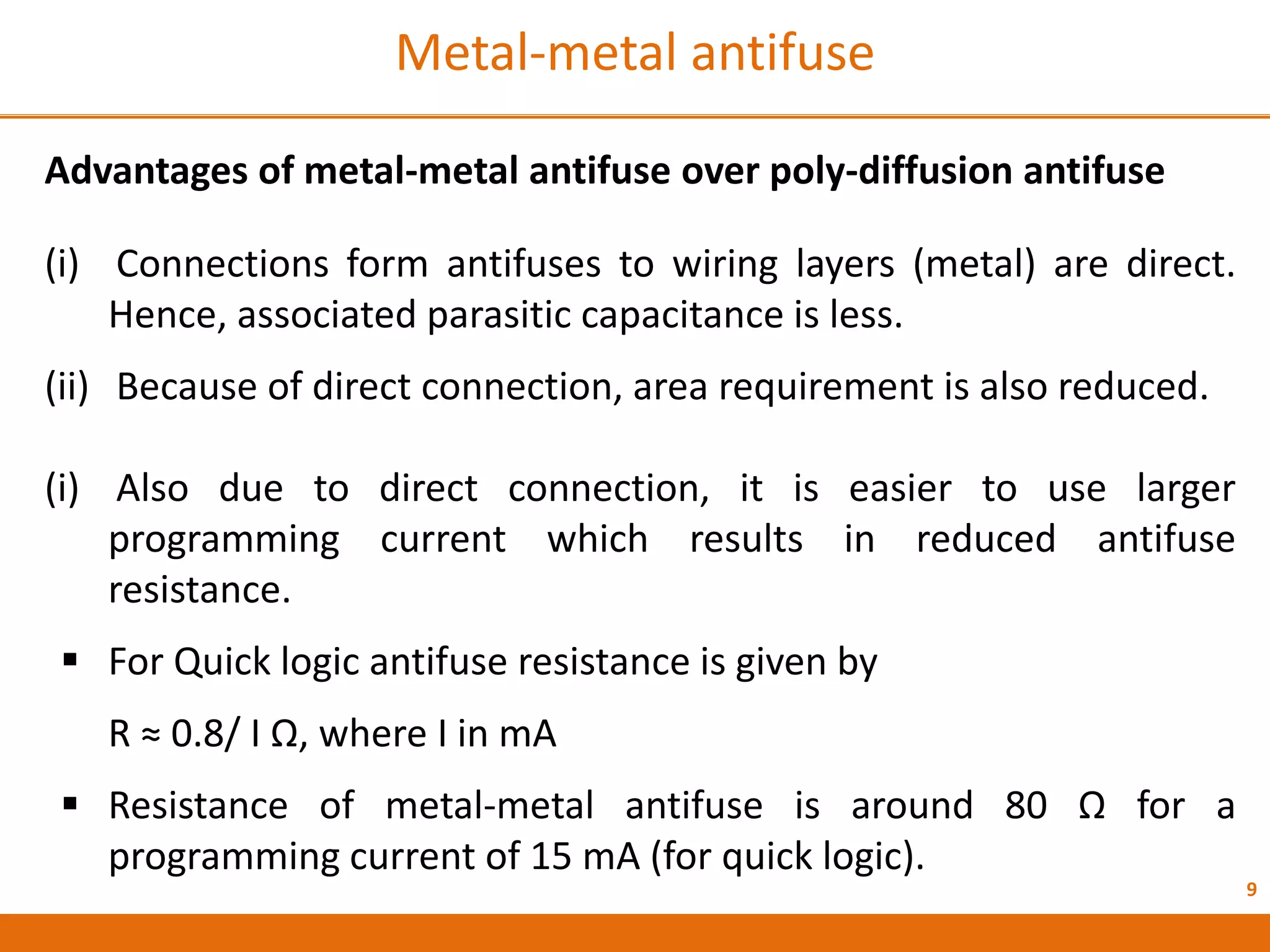
Description of the metal-metal antifuse technology by Quick Logic, its advantages over poly-diffusion.
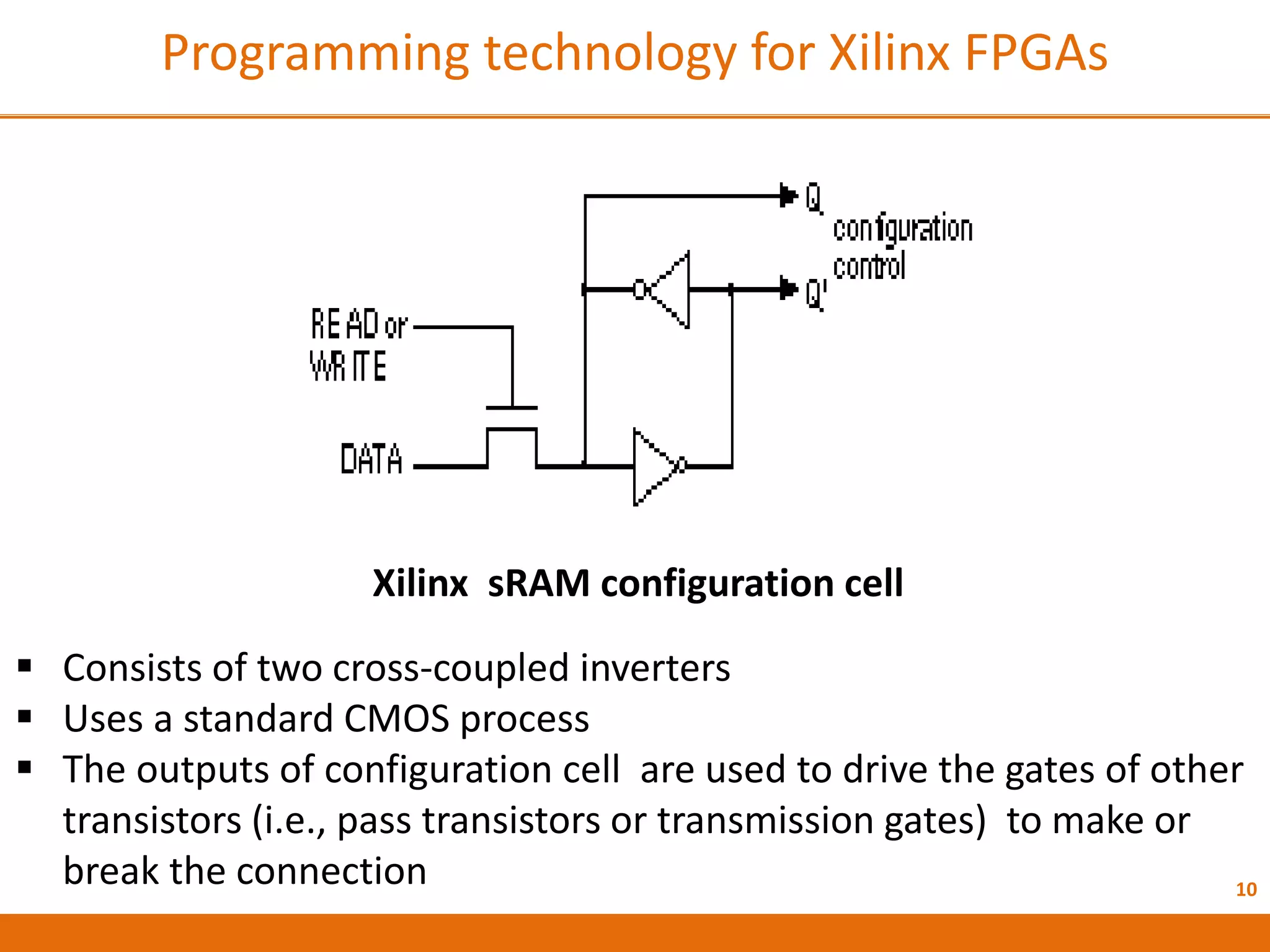
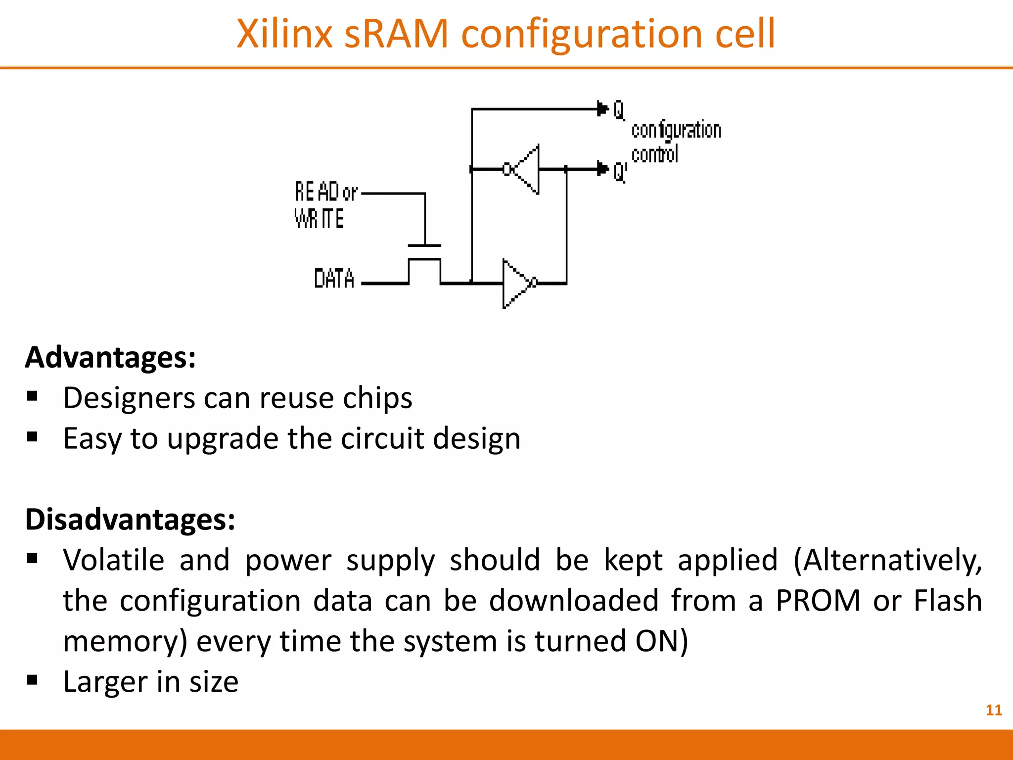
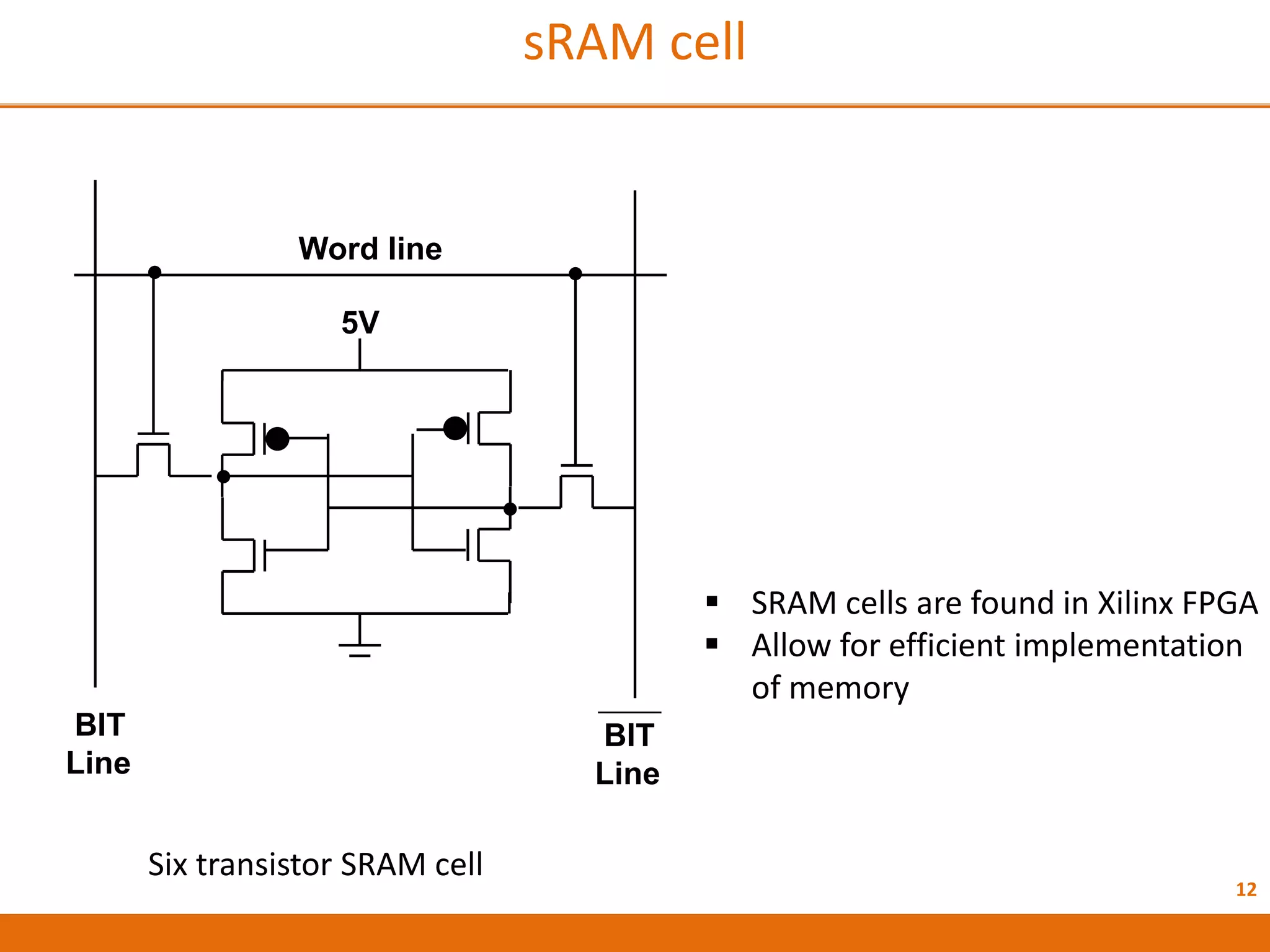
Xilinx FPGA programming using SRAM cells, their configuration, advantages, and disadvantages.
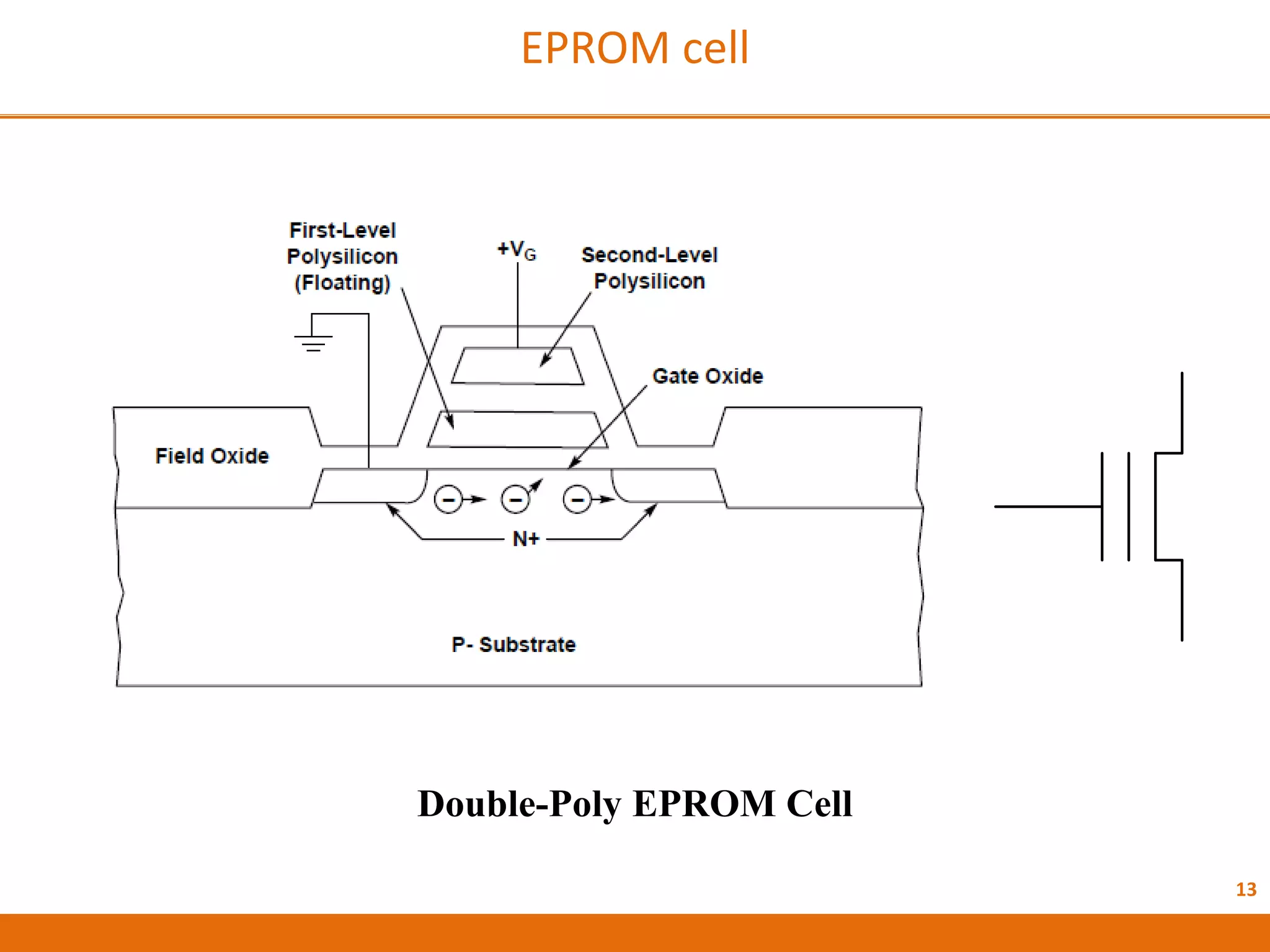
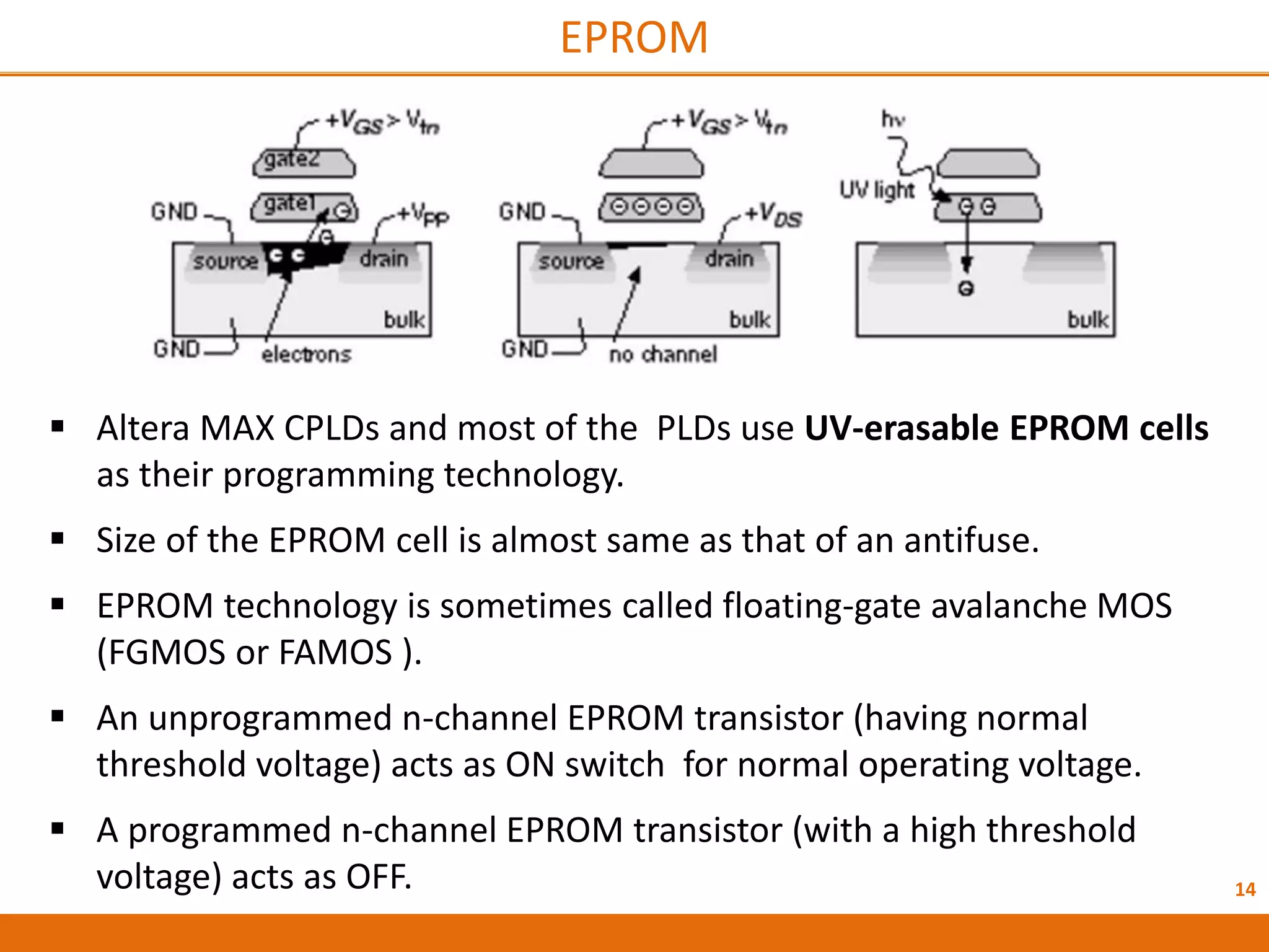
Introduction to EPROM cell technology used in Altera MAX CPLDs, including size and functionality.
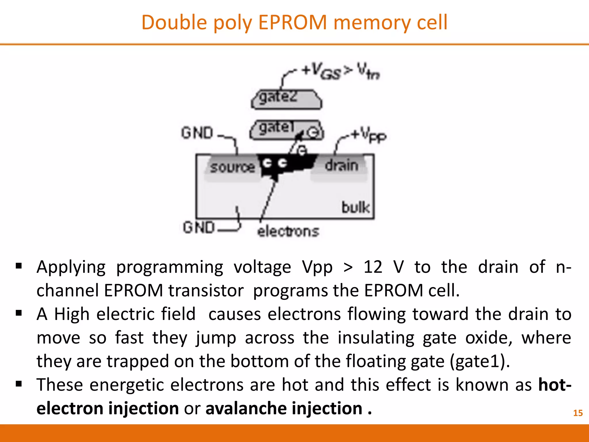
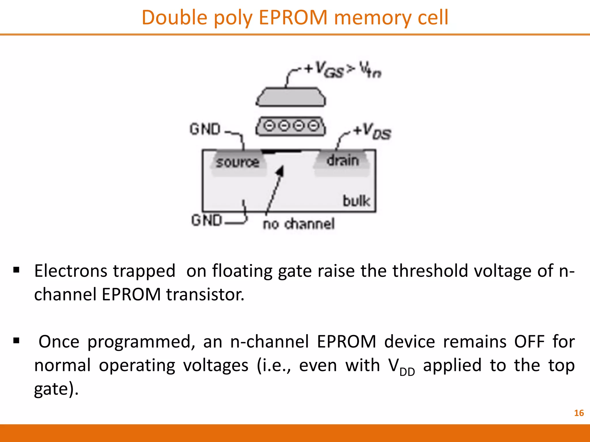
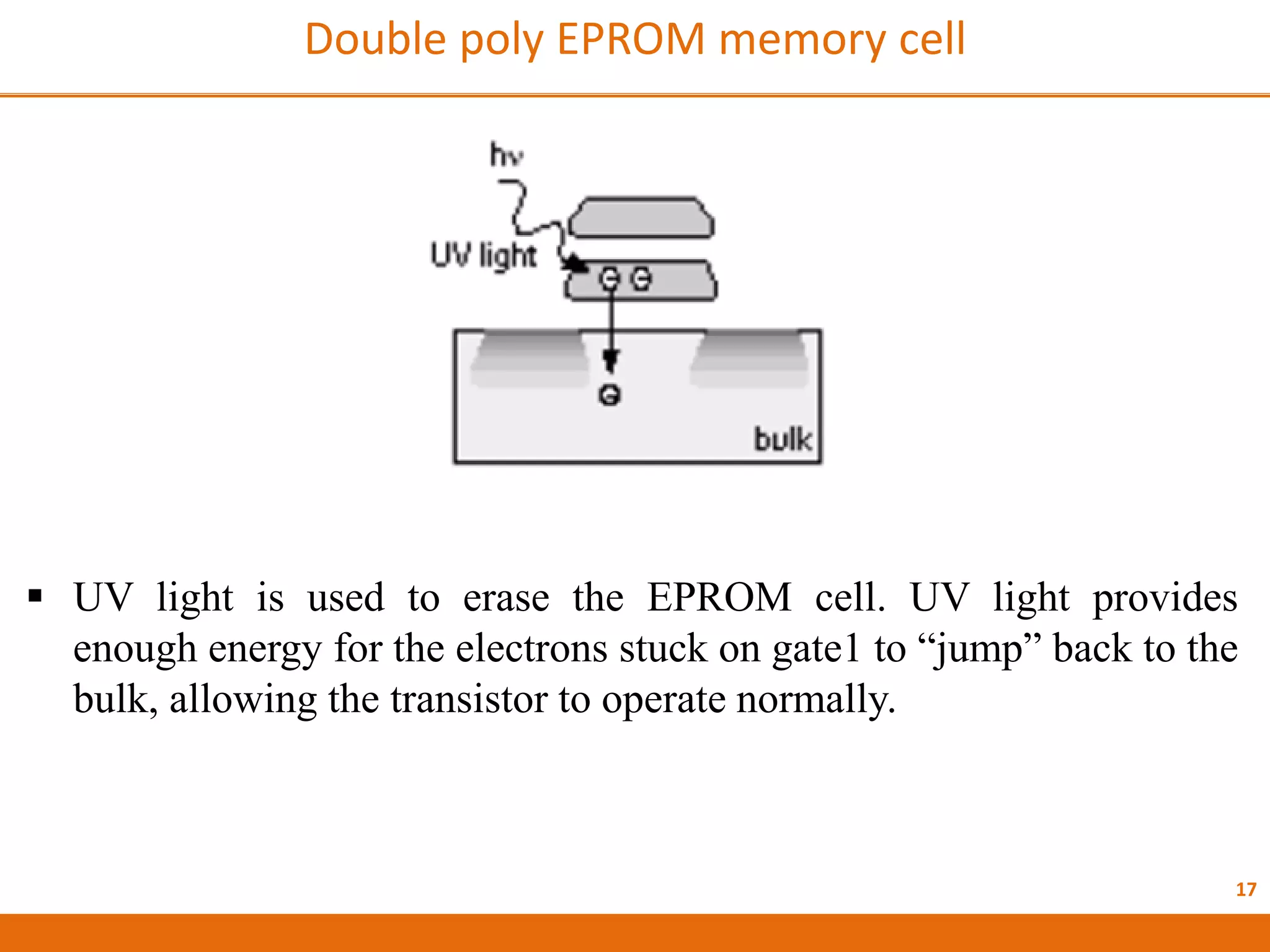
Details on programming and erasing mechanisms of double-poly EPROM memory cells.
Explanation of EEPROM programming and erasing process compared to EPROM technology.
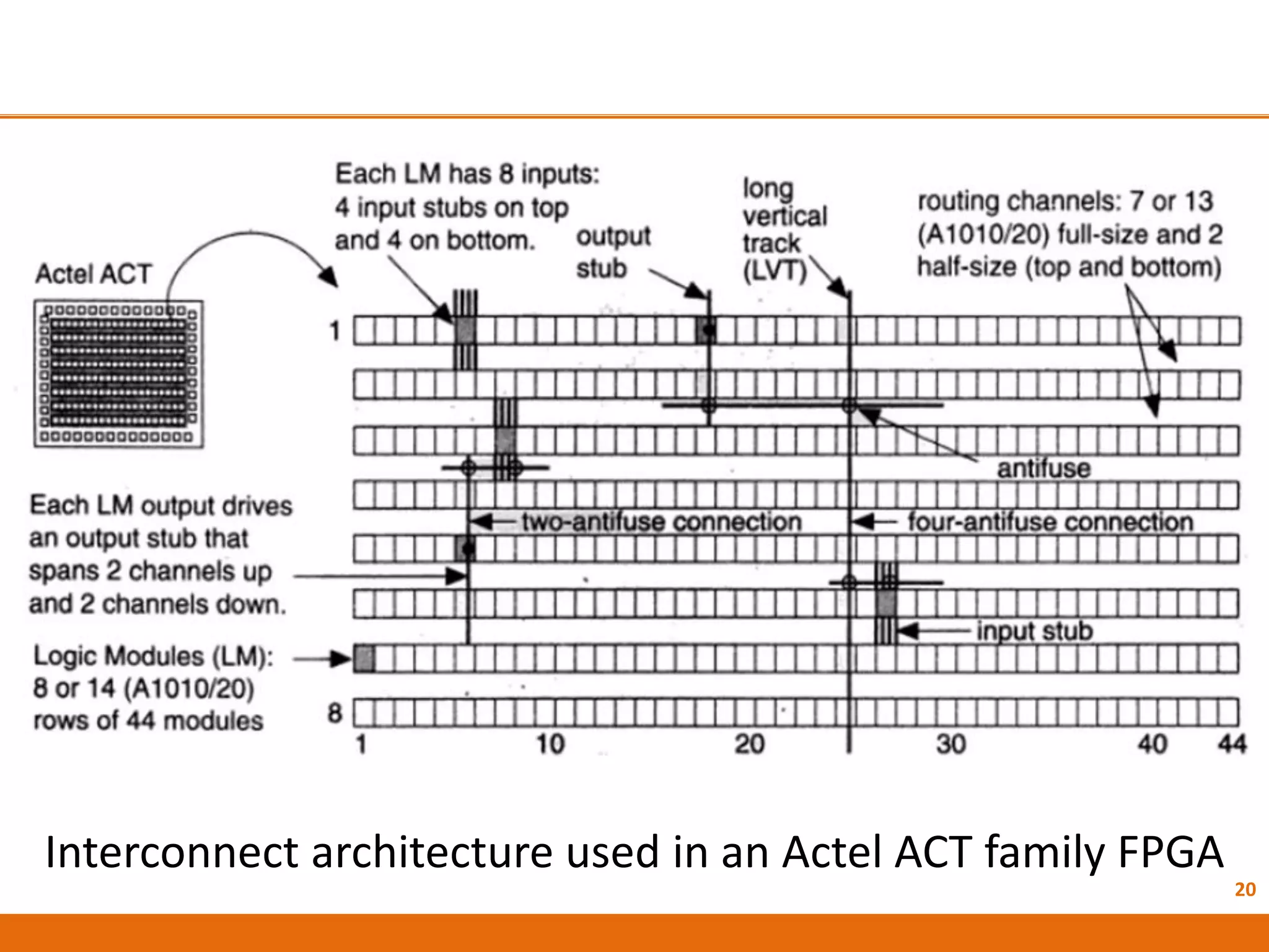
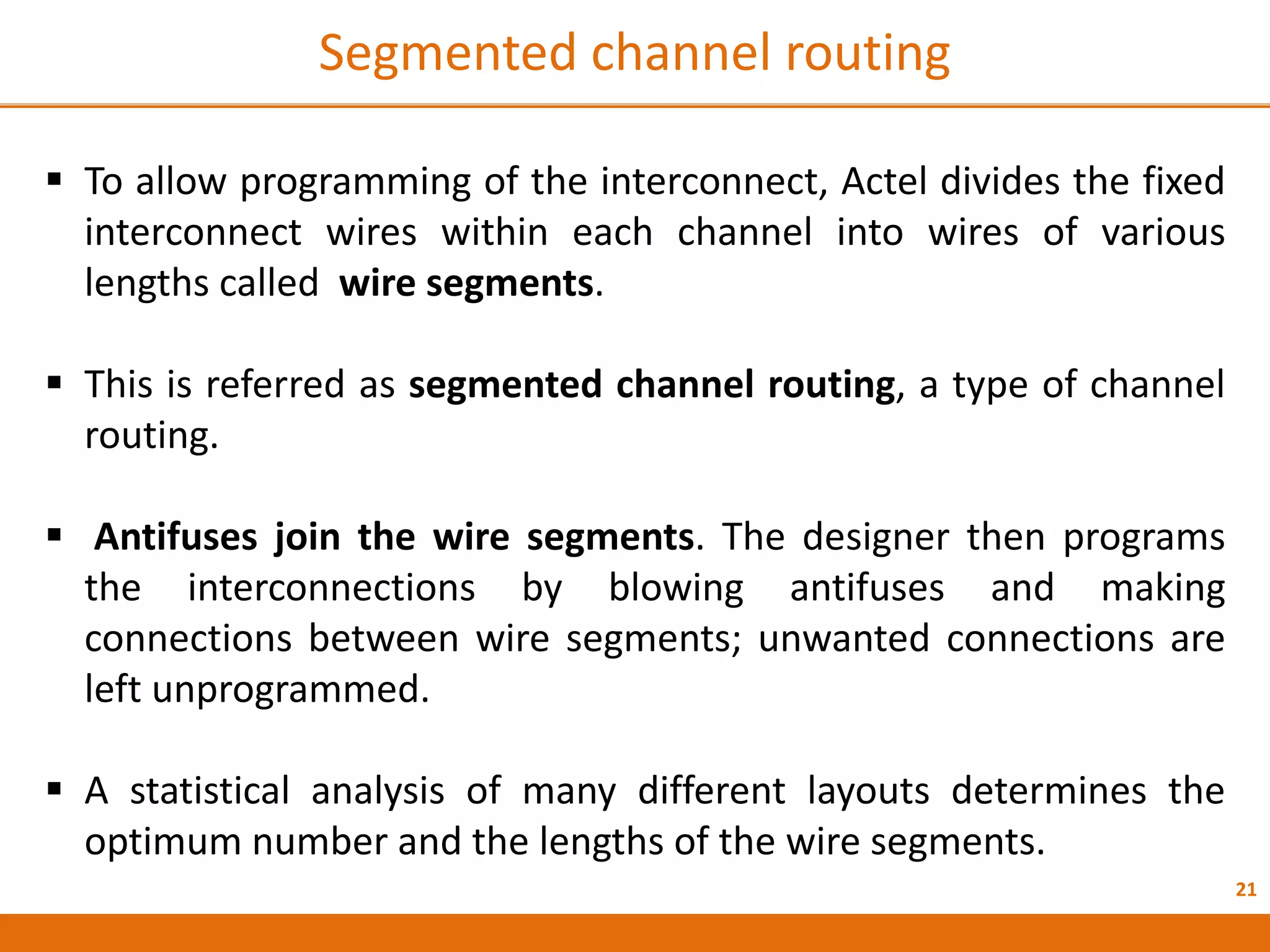
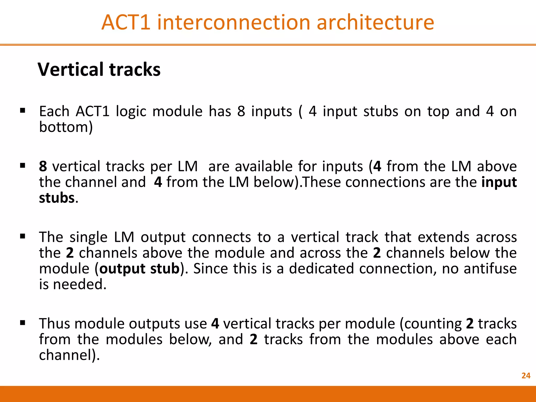
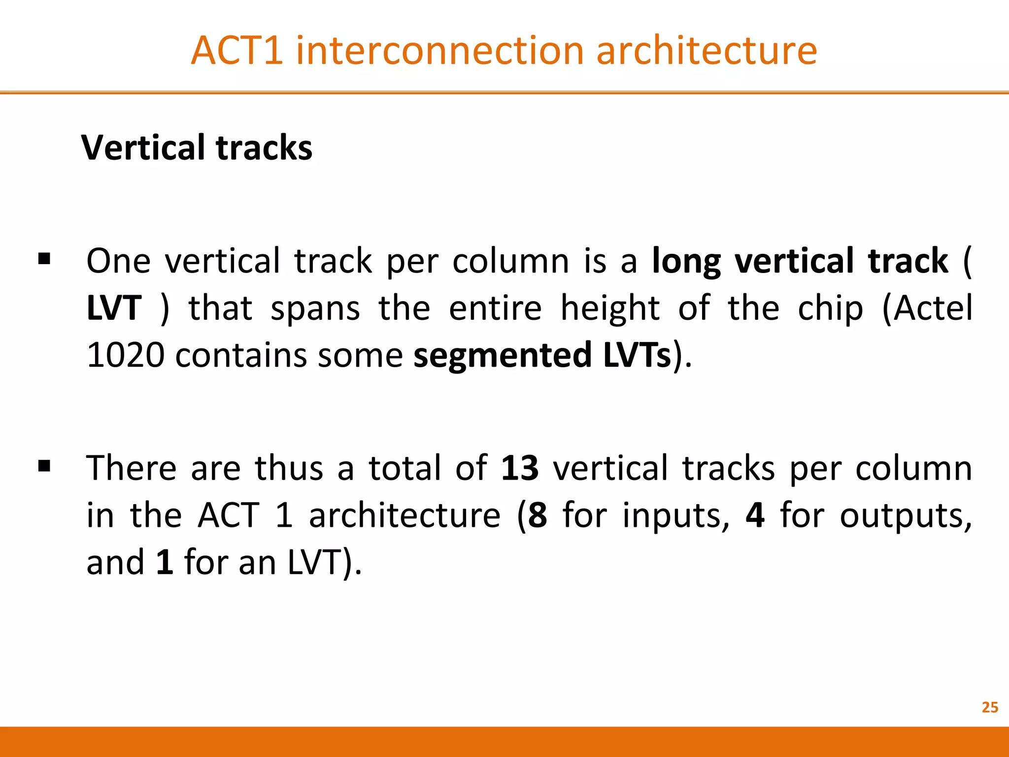
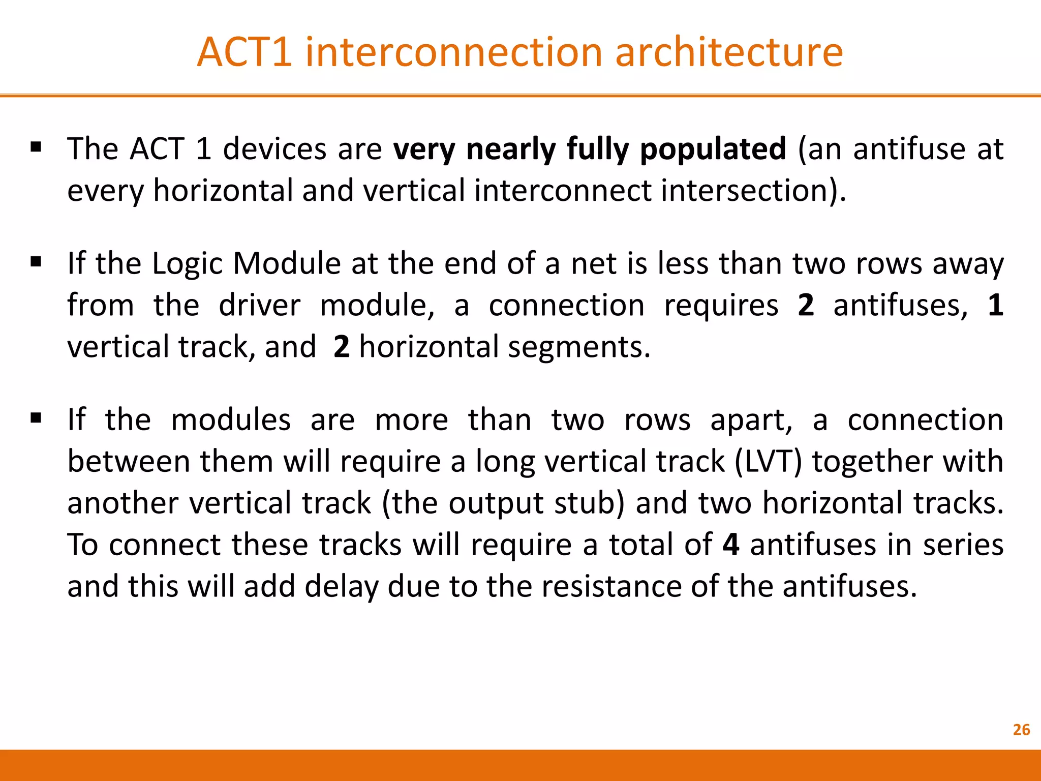
Description of ACTEL's interconnect routing channels and the concept of segmented channel routing.
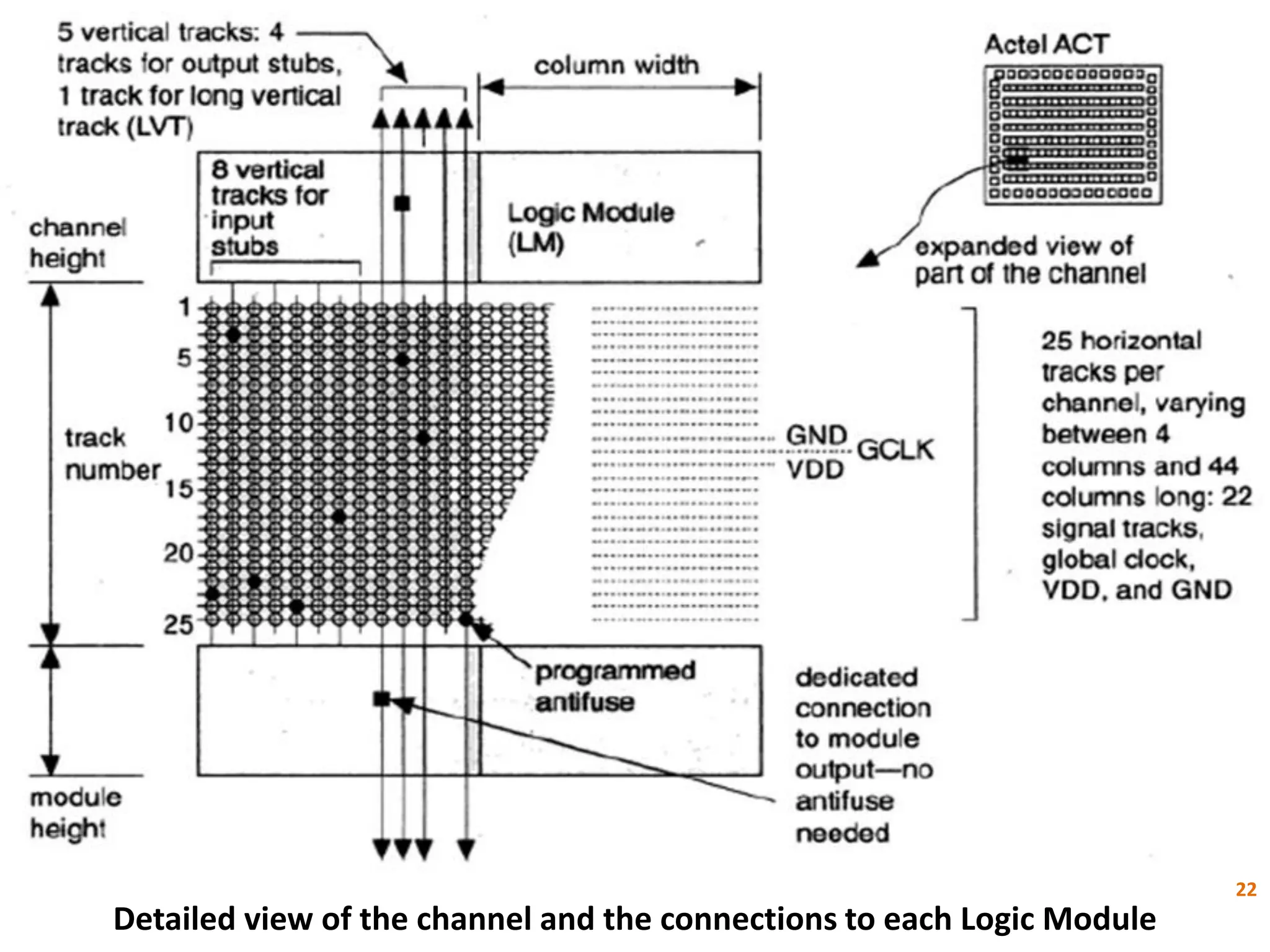
Detailed layout of horizontal and vertical tracks in ACTEL architecture, and antifuse connection details.
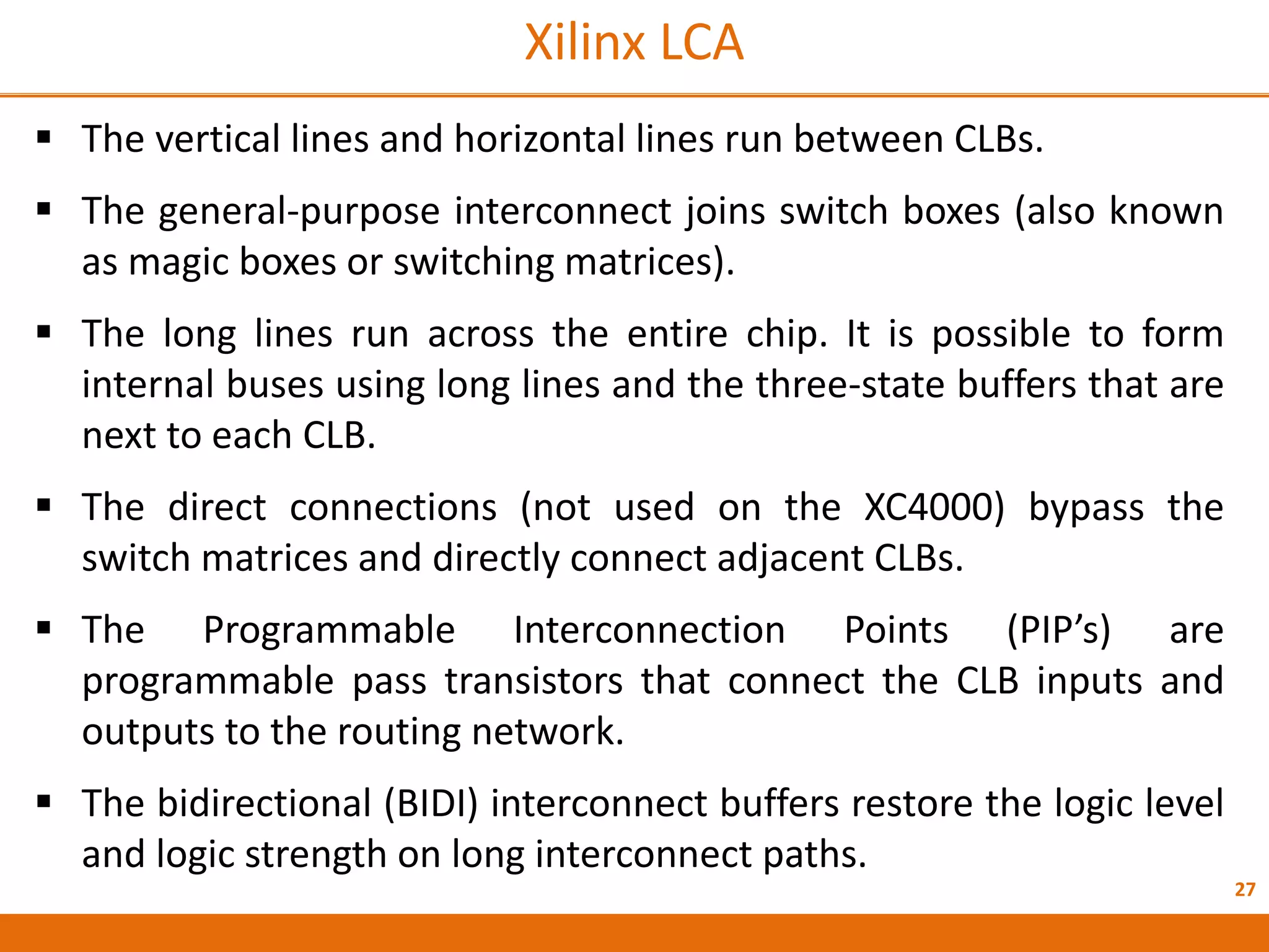
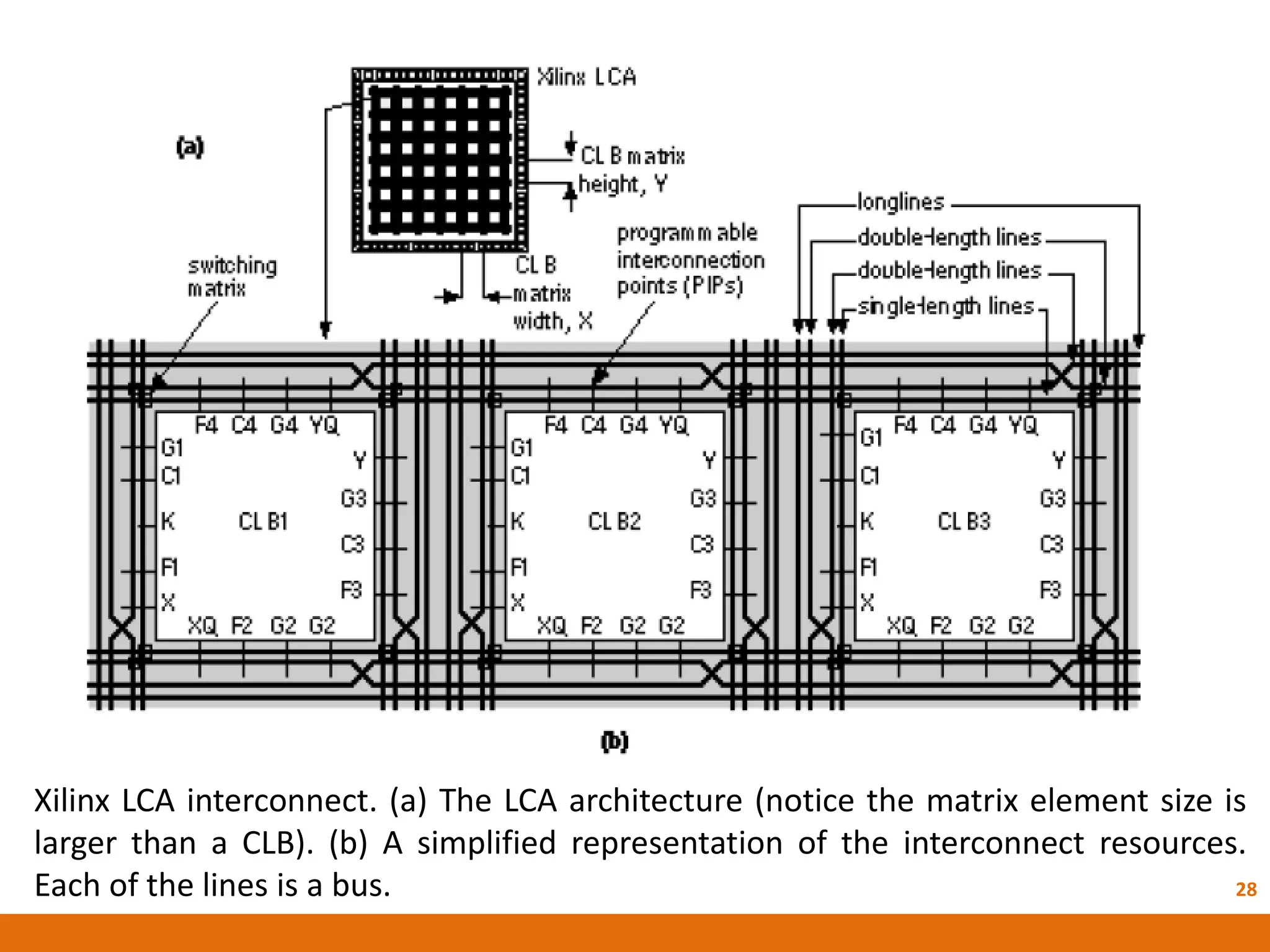
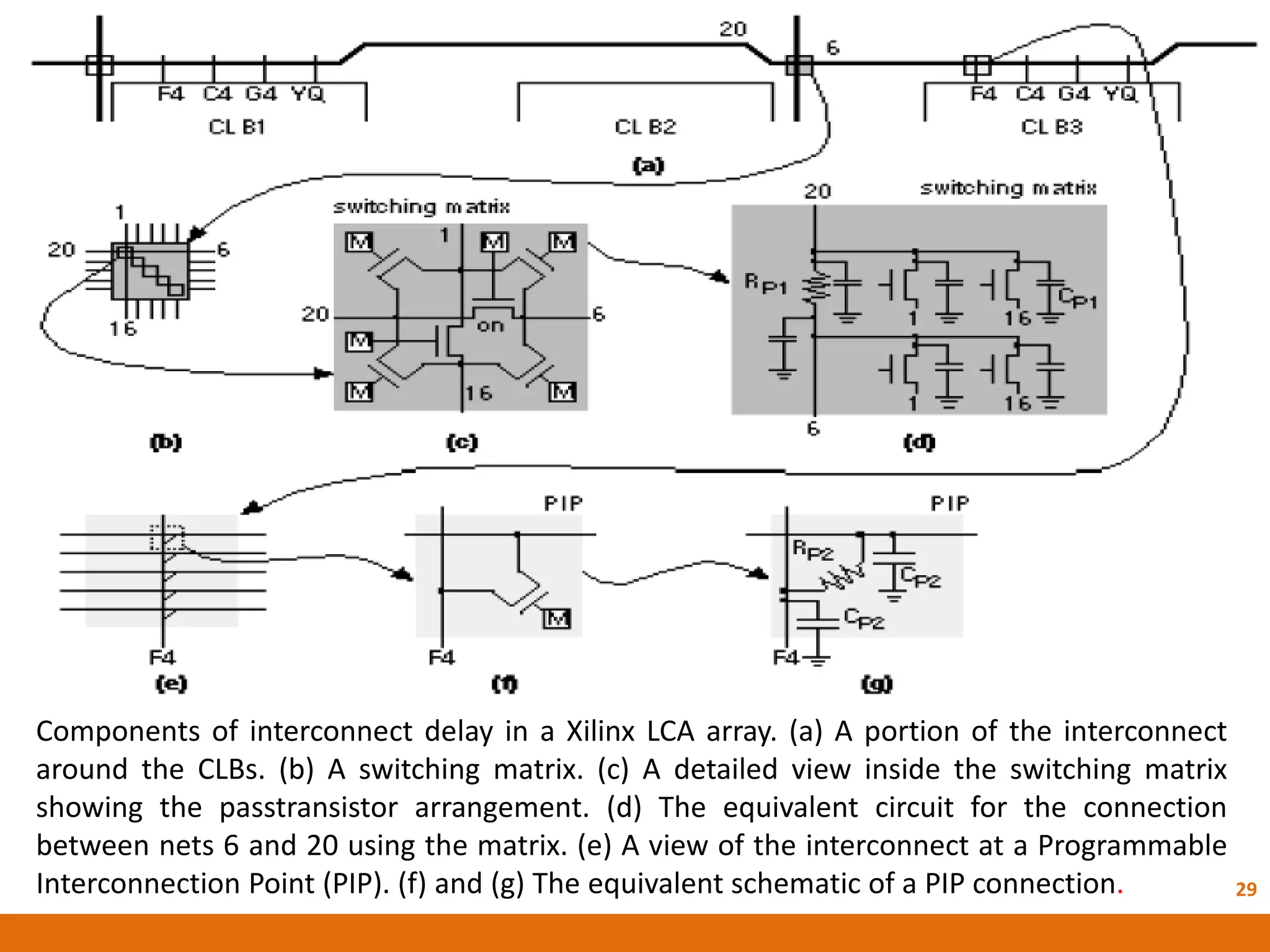
Overview of Xilinx LCA interconnect, programmable interconnection points, and components of interconnect delay.
Description of Altera MAX interconnect scheme using Programmable Interconnect Array for consistent delay.
Contact information for Dr. D.V. Kamath for further inquiries regarding the presentation.