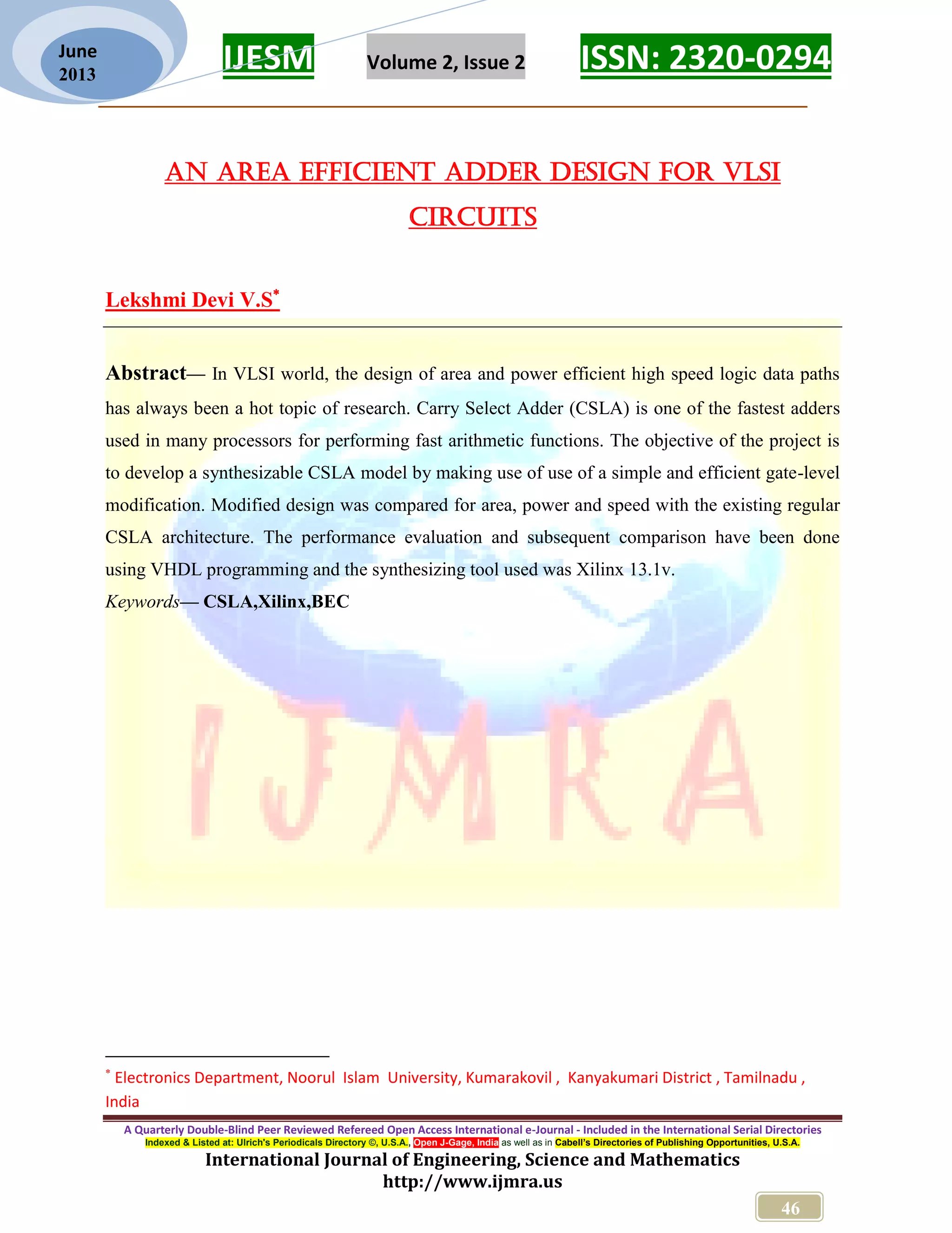
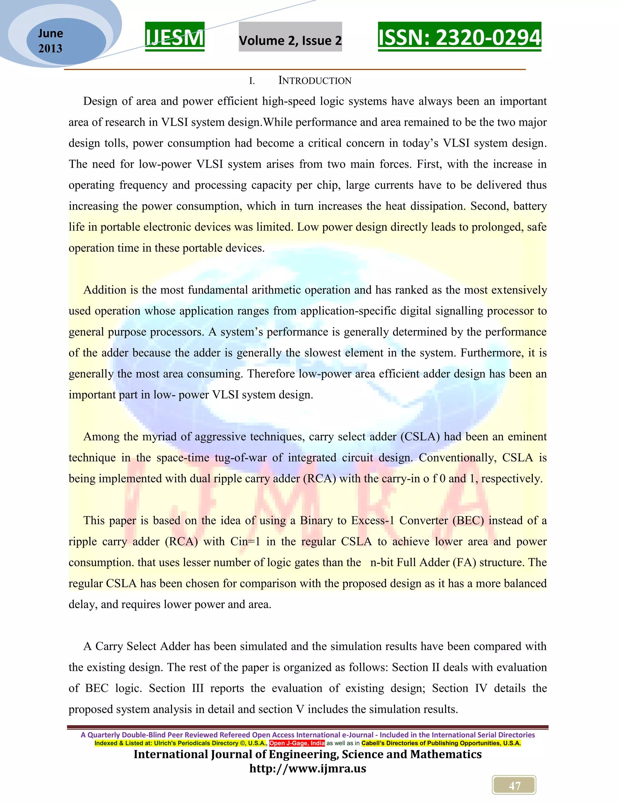
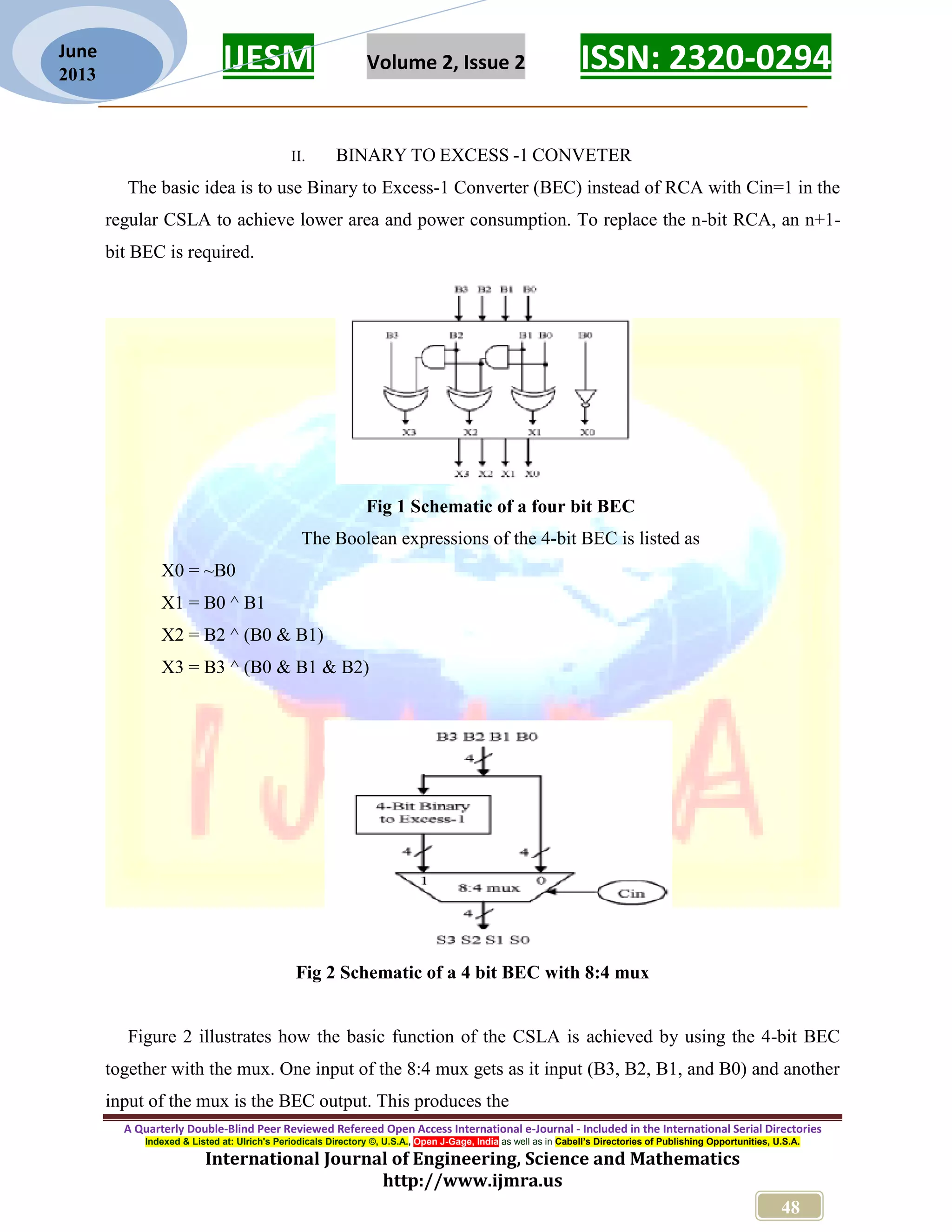
This document discusses the design and performance evaluation of a modified carry select adder (CSLA) for VLSI circuits, aimed at improving area efficiency and power consumption compared to traditional designs. The proposed method incorporates a binary to excess-1 converter (BEC), replacing conventional ripple carry adders to reduce gate count and delay. Simulation results demonstrate that the modified CSLA achieves a significant reduction in gate area with a minimal increase in delay, indicating its effectiveness for low-power applications.
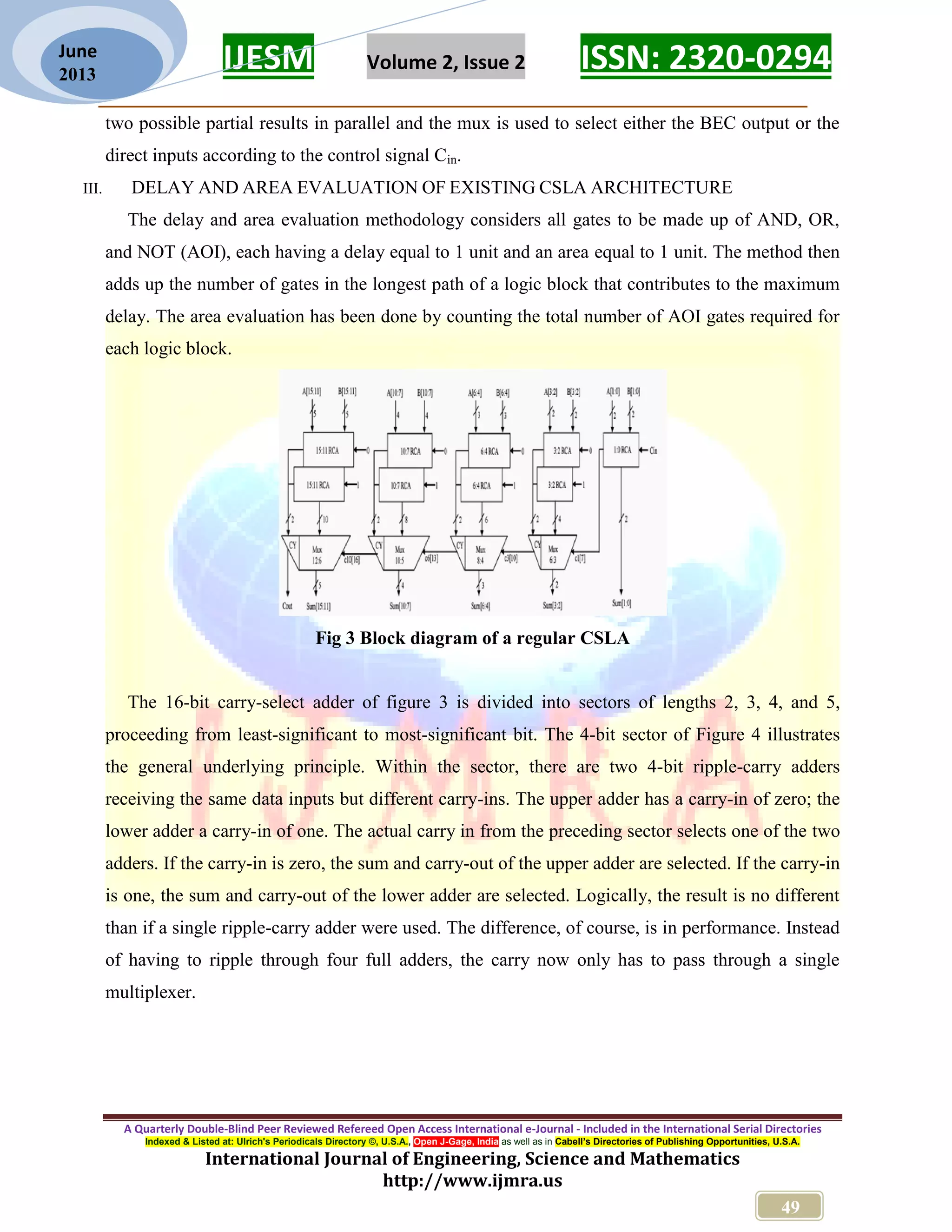
![IJESM Volume 2, Issue 2 ISSN: 2320-0294 _________________________________________________________ A Quarterly Double-Blind Peer Reviewed Refereed Open Access International e-Journal - Included in the International Serial Directories Indexed & Listed at: Ulrich's Periodicals Directory ©, U.S.A., Open J-Gage, India as well as in Cabell’s Directories of Publishing Opportunities, U.S.A. International Journal of Engineering, Science and Mathematics http://www.ijmra.us 50 June 2013 Fig 4 Four bit sector schematic Fig 5 Detailed internal schematic of a regular 16-bit CSLA The detailed internal architecture of a 16-bit conventional CSA is shown in Figure 5. It has 17-half adders and 15-full adders. Since the ripple carry adder (RCA) is used in the final stage, this structure yields large carry propagation delay. To reduce this delay, the final stage of CSA is divided into 5 groups .The first group includes 1+ log2n bit value and other groups include log2n bit value, where n is the bit size of the adder. The divided groups are listed below. i). c4, s [4:0] ii). c7, x [7:5] iii). c10, x [10:8] iv). c13, x [13:11] v). x [17:14] The first group of output s[4:0] are directly assigned as the final output; the second group c7,x[7:5] manipulates the partial result by considering c4 is zero; the third group c10,x[10:8]](https://image.slidesharecdn.com/5ijmra-esm3169-170815135824/75/An-Area-Efficient-Adder-Design-for-VLSI-Circuits-5-2048.jpg)
![IJESM Volume 2, Issue 2 ISSN: 2320-0294 _________________________________________________________ A Quarterly Double-Blind Peer Reviewed Refereed Open Access International e-Journal - Included in the International Serial Directories Indexed & Listed at: Ulrich's Periodicals Directory ©, U.S.A., Open J-Gage, India as well as in Cabell’s Directories of Publishing Opportunities, U.S.A. International Journal of Engineering, Science and Mathematics http://www.ijmra.us 51 June 2013 manipulates the partial result by considering c7 is zero; the fourth group c13,x[13:11] manipulates the partial result by considering c10 is zero and the fifth group x[17:14] manipulates the partial result by considering c13 is zero.Based on this approach, the delay and area evaluation of the CSLA adder block consisting of 2:1 mux, Half Adder (HA), and Full Adder (FA) are evaluated and listed in Table 1 Table 1 Delay and area evaluation results of various gates in the adder block group 1 group 2 group 3](https://image.slidesharecdn.com/5ijmra-esm3169-170815135824/75/An-Area-Efficient-Adder-Design-for-VLSI-Circuits-6-2048.jpg)
![IJESM Volume 2, Issue 2 ISSN: 2320-0294 _________________________________________________________ A Quarterly Double-Blind Peer Reviewed Refereed Open Access International e-Journal - Included in the International Serial Directories Indexed & Listed at: Ulrich's Periodicals Directory ©, U.S.A., Open J-Gage, India as well as in Cabell’s Directories of Publishing Opportunities, U.S.A. International Journal of Engineering, Science and Mathematics http://www.ijmra.us 52 June 2013 group 4 Fig 5 Delay and Area Evaluation of different stages of regular CSLA The group2 has two sets of 2 bit RCA. The arrival time of selection input c1 [time (t) = 7] of 6:3 mux is earlier than s3 [t = 8] and later than s2 [t = 6]. Thus, sum3 [t = 11] is the summation of s3 and mux [t= 3].Similarly, sum2 [t = 10] is the summation of c1 and mux. Except for group2, the arrival time of mux selection input is always greater than the arrival time of data outputs from the RCA’s.Thus,the delay of group3 togroup5 can be determined, respectively as follows: c6, sum [6 : 4] = c3 [t = 10] + mux c10, sum [10 : 7] = c6 [t = 13] + mux Cout, sum [15: 11] = c10 [t = 16] + mux. The one set of 2-bit RCA in group2 has 2 FA for Cin=1 and the other set has one FA and one HA for Cin=0. Based on the area count of Table I, the total number of gate counts in group2 can be determined as follows and is listed in Table II Gate count =57 (FA +HA + Mux) FA=39 HA=6 Mux=12](https://image.slidesharecdn.com/5ijmra-esm3169-170815135824/75/An-Area-Efficient-Adder-Design-for-VLSI-Circuits-7-2048.jpg)
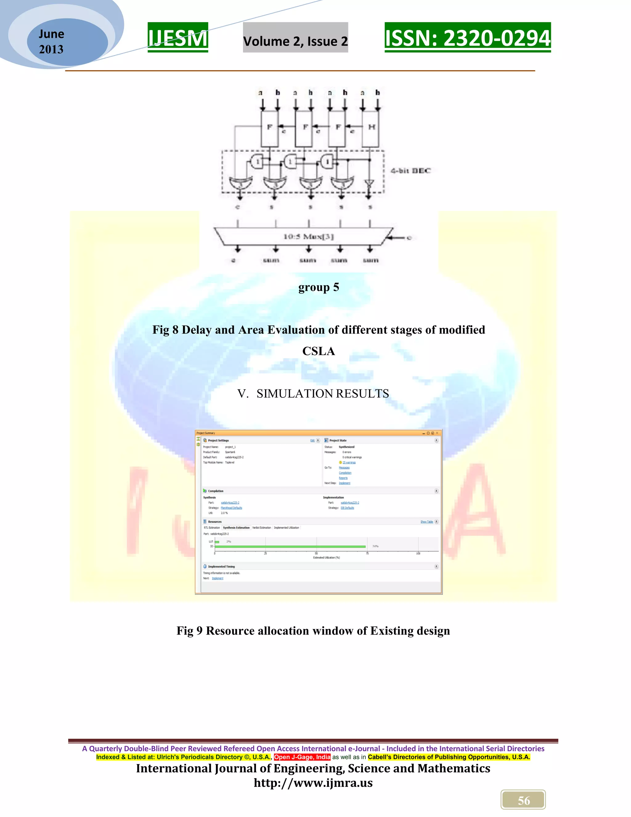
![IJESM Volume 2, Issue 2 ISSN: 2320-0294 _________________________________________________________ A Quarterly Double-Blind Peer Reviewed Refereed Open Access International e-Journal - Included in the International Serial Directories Indexed & Listed at: Ulrich's Periodicals Directory ©, U.S.A., Open J-Gage, India as well as in Cabell’s Directories of Publishing Opportunities, U.S.A. International Journal of Engineering, Science and Mathematics http://www.ijmra.us 54 June 2013 Here also, the design is spitted into 5 different stages and area and delay are evaluated as it had done previously. The delay and area estimation of each group are shown in Figures (a) through (d).The steps leading to the evaluation are. The group2 has one 2-bit RCA which consists of one FA and one HA for Cin=0.Instead of another 2 bit RCA with Cin=1, a 3 bit BEC is used which adds one to the output from 2 bit RCA. Based on the consideration of delay values of Table I, the arrival time of selection input c1 [t=7] of 6:3 mux is earlier than the s3 [t=9] and c3 [t=10] and later than the s2 [t=4]. Thus, the sum3 and final c3 (output from mux) are depending on s3 and mux and partial c3 (input to mux) and mux, respectively. The sum2 depends on c1 and mux2 For the remaining group’s the arrival time of mux selection input is always greater than the arrival time of data inputs from the BEC’s.Thus, the delay of the remaining groups depends on the arrival time of mux selection input and the mux delay. Similarly, the estimated maximum delay and area of the other groups of the modified CSLA are evaluated and listed in Table III.Comparing the tables, it is clear that the proposed modified CSLA saves 113 gate areas than the regular CSLA, with only 11 increases in gate delays. Table III Area and Delay evaluation results of various sections of Modified CSLA](https://image.slidesharecdn.com/5ijmra-esm3169-170815135824/75/An-Area-Efficient-Adder-Design-for-VLSI-Circuits-9-2048.jpg)
![IJESM Volume 2, Issue 2 ISSN: 2320-0294 _________________________________________________________ A Quarterly Double-Blind Peer Reviewed Refereed Open Access International e-Journal - Included in the International Serial Directories Indexed & Listed at: Ulrich's Periodicals Directory ©, U.S.A., Open J-Gage, India as well as in Cabell’s Directories of Publishing Opportunities, U.S.A. International Journal of Engineering, Science and Mathematics http://www.ijmra.us 59 June 2013 REFERENCES 1]. Padma Devi, Ashima Girdher, Balwinder Singh, “Improved Carry Select Adder with Reduced Area and Low Power Consumption”, International journal of computer applications (0975 – 8887) volume 3 – no.4, June 2010. ` [2].Youngjoon Kim and Lee-Sup Kim,” Low Power Carry Select AdderWith Reduced Area”, IEEE J.Solid-State Circuits, vol. 36, no. 10, pp. 1538–1545, Oct. 2001 [3].B.Ramkumar, Harish M Kittur, P.Mahesh Kannan,”Asic Implementation Of Modified Faster Carry Save Adder”, European Journal of Scientific Research Wassn 1450-216x Vol.42 No.1 (2010). [4].I-Chin Wey,Cheng-chen ho,YI-sheng lin,Chien-chang pen,“An Area-Efficient Carry Select Adder Design By Sharing The Common Boolean Logic Term”, IEEE Trans. Circuits Syst. II, Analog Digit. Signal Process. vol. 49, no. 1, pp. 16–24, Jan. 2002. [5].N. Ravikumar1, M. Vishwanath, B. Durga Malleswara Reddy, “An Area Efficient 32-Bit Carry-Select Adder For Low Power Applications”, International Journal Of Computer&Communication Technology (Ijcct), Vol.-3, Wassue - 4, 2012. [6].BehnamAmelifard,,FarzanFallah,Massoud Pedram,”Closing The Gap Between Carry Select Adder And RippleCarryAdder:](https://image.slidesharecdn.com/5ijmra-esm3169-170815135824/75/An-Area-Efficient-Adder-Design-for-VLSI-Circuits-14-2048.jpg)