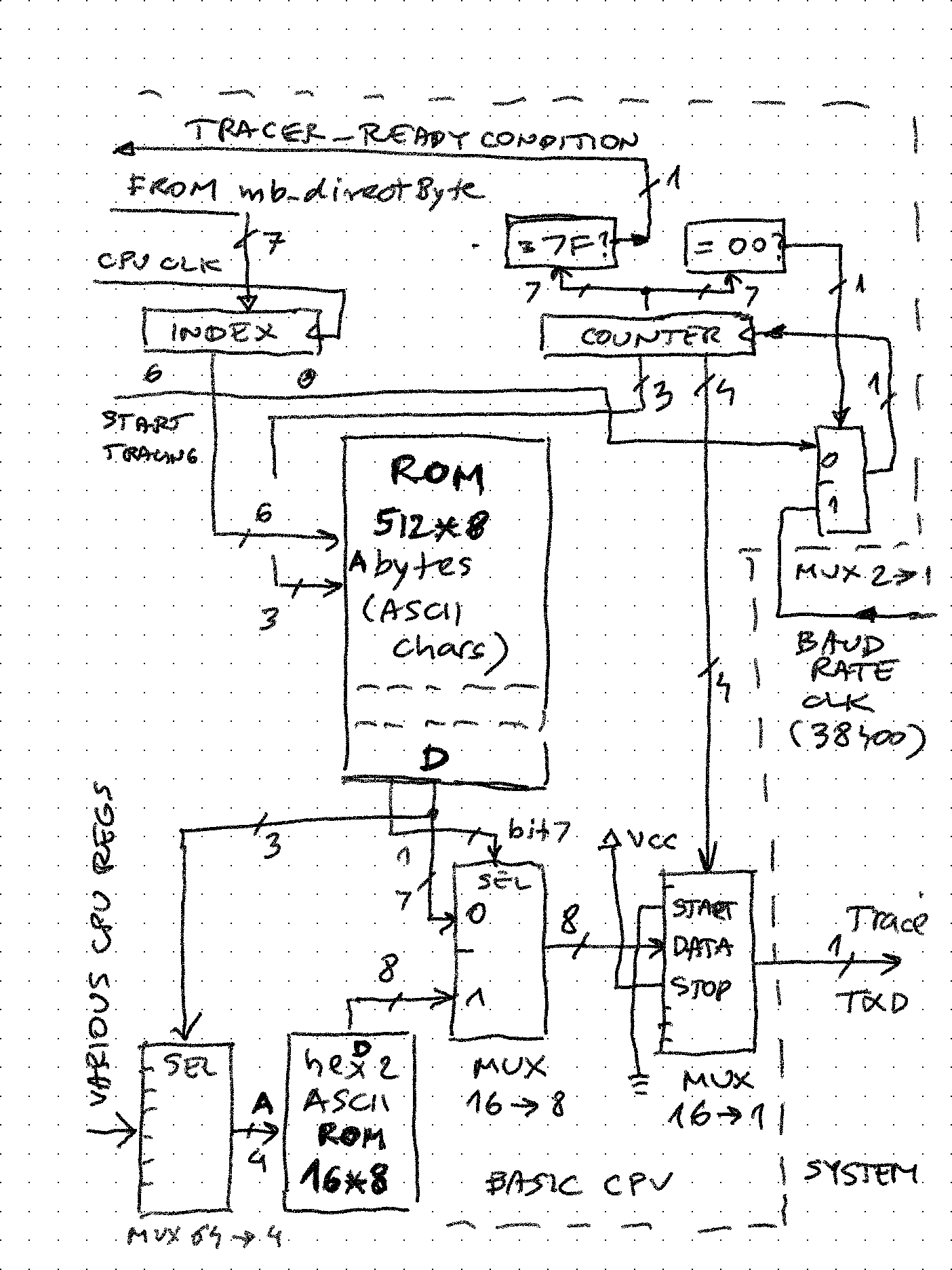
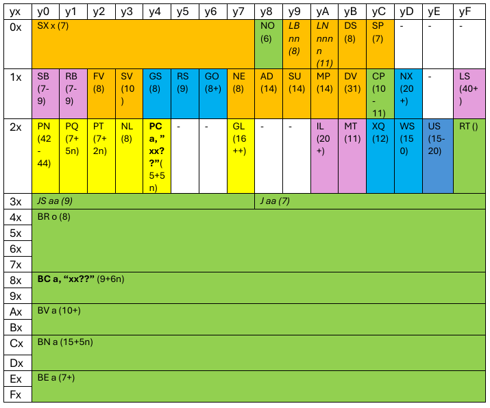
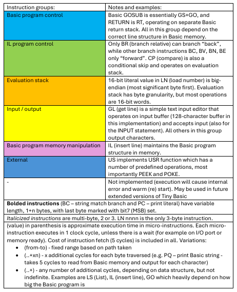
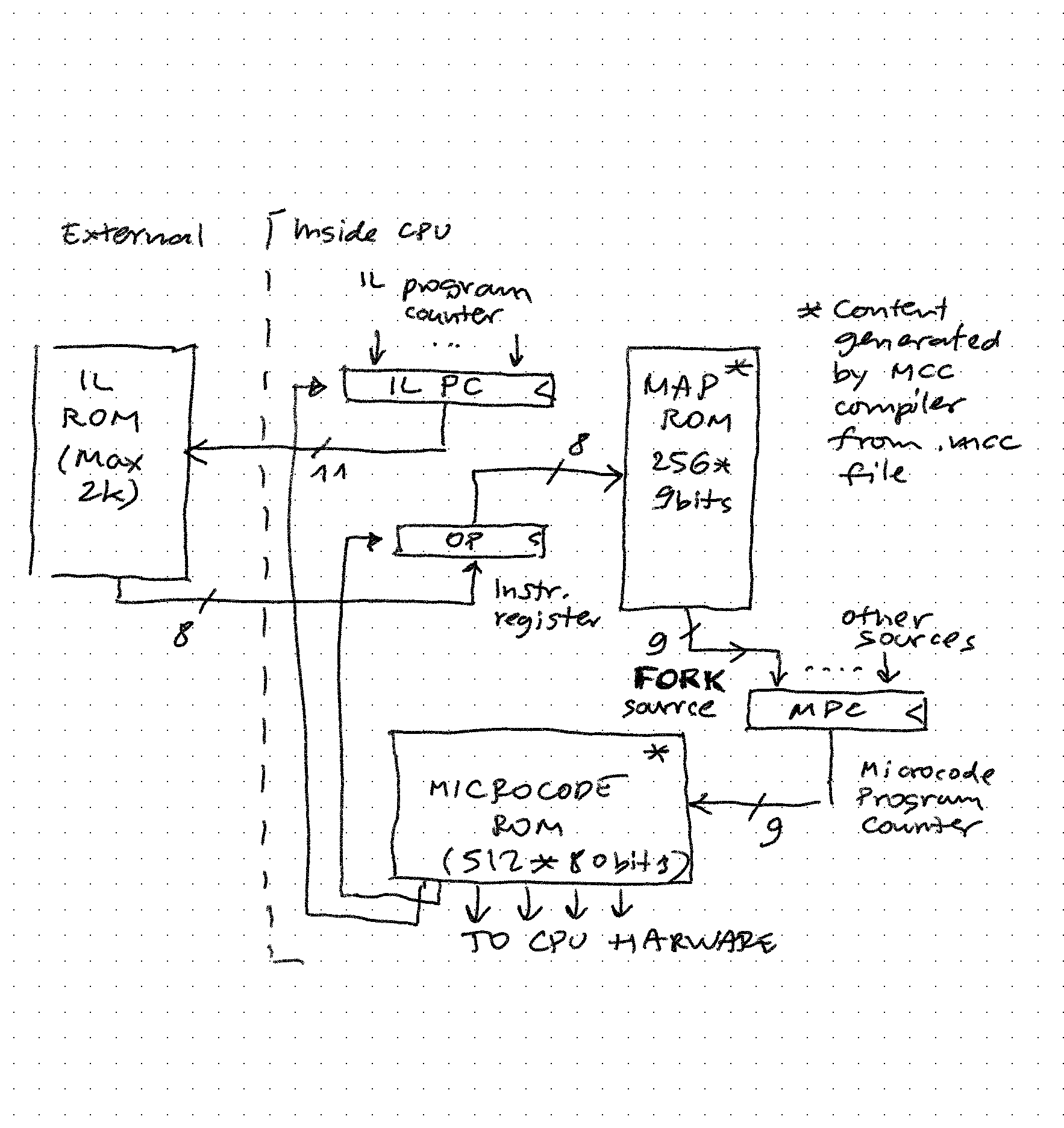
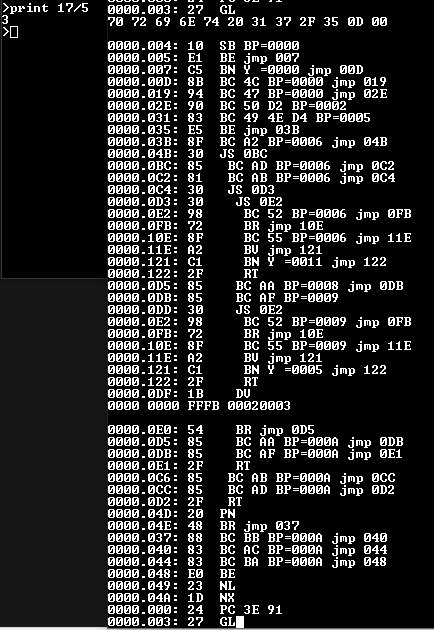
By implementing a custom micro-coded CPU that executes it directly (up to 100MHz)
To make the experience fit your profile, pick a username and tell us what interests you.
We found and based on your interests.
marquee_demo.basDisplays "Hello world" (or any other text) as marquee on VGA (only works if the core memory is visualized through some display device)bas - 1.08 kB - 11/17/2025 at 04:28 | | |
hexdump.basHexDump program from http://www.ittybittycomputers.com/IttyBitty/TinyBasic/TBuserMan.txtbas - 2.13 kB - 11/17/2025 at 04:21 | | |
benchmark_mag - tiny.basFirst 1000 primes benchmark - with GOTO onlybas - 873.00 bytes - 11/17/2025 at 04:20 | | |
benchmark_lalu - tiny.basFirst 1000 primes benchmark - with GOSUBbas - 912.00 bytes - 11/17/2025 at 04:20 | | |
sys_microbasic_anvyl.bitBinary for direct download (will work only on Digilent Anvyl board)bit - 1.42 MB - 11/17/2025 at 04:20 | |
I was really curious how the Basic CPU will perform in comparison with classic CPUs of the home computer era and put some effort into optimizing the design with that goal in mind. Based on the benchmark tests, the goal has been only partially achieved. While in some cases the speed up of factor 4 to 8 looks noteworthy, my suspicion is that those Basic interpreters by default work with software - implemented floating point for the benchmark test (haven't explored them in depth), while other group showing more modest gain of 1.5 to 2X are "integer Basic" implementations, and a more fair comparison.
CPU performance optimizations I used:
A bit of "cheating" going on here - whole design is inside the FPGA which allows it to work at maximum available hardware clock frequency of 100MHz. Most importantly, the "core" RAM (Basic input buffer and program store) can be accessed in 1 or 2 clock cycles (so 10 or 20ns):
writeCore: nWR = 0, if nBUSACK then repeat else return; readCore: nRD = 0, if nBUSACK then repeat else next; nRD = 0, MDR <= from_Bus, back; This would clearly be impossible if the RAM is outside of the FPGA, even on the same board. Depending on the CPU clock and memory speed, one or more wait cycles would need to be added. Anvyl board has a breadboard section, so in future I may move the Basic core memory to a 62256 type device and experiment for example how many wait cycles does a 70ns vs. 120ns memory chip need.
Other limiting factor is I/O speed. Currently, max I/O serial speed is 38400 bps. Sending and receiving 1 byte over such channels takes at least 10-bit times, during which CPU has to wait for the ready signal.
outChar: if CHAROUT_READY then next else repeat; // sync with baudrate clock if CHAROUT_READY then return else repeat; FIFO queue on both input and output would help, but their implementation belongs to the Ser2Par and Par2Ser components, not the CPU (except for the trace serial output, but that one is only active up to 4kHz CPU frequency so not much gained there).
Basic CPU is a CISC processor, and pipelining is not traditionally their strength. However a very limited opportunity of overlap is used between execute and fetch in few instructions. Note that the fetch cycle has two entry points:
fetch: traceString 51; // CR, LF, then trace Basic line number (in hex, for speed) fetch1: traceString 2; // trace IL_PC and future opcode IL_OP <= from_interpreter, IL_PC <= inc, traceSDepth; // load opcode, advance IL_PC, indent by stack depth IL code if tracing is on T <= zero, alu <= reset0, if IL_A_VALID then fork else INTERNAL_ERR; // jump to entry point implementing the opcode (or break if we went into the weeds) Most instructions finish their execute cycle and then branch back to "fetch" (no overlap). Few have the opportunity to execute "traceString 51" operation while in parallel doing other operations, and when done can branch to "fetch1" - this is a 1 clock cycle overlap. This could be utilized more, but tracing at the beginning of fetch cycle is very convenient debug tool, so this was an engineering compromise between 2 important goals (troubleshooting and performance).
//////////////////////////////////////////////////////////////////////////////// .map 0x12; // FV (Fetch Variable) //////////////////////////////////////////////////////////////////////////////// traceString 36; // trace mnemonic Vars <= indexFromExpStack, if STACK_IS_EMPTY then ESTACK_ERR; // get index (variable name A-Z) T <= from_vars, ExpStack <= pop1, traceString 51; // T <= Vars(index) ExpStack <= push_TWord, goto fetch1; // push onto stack, go to 2rd fetch entry point as we overlapped 1 cycle Basic CPU uses "horizontal microcode" with fairly wide control word of 80 bits:
Complex programmable logic designs are opaque. Unless this opaqueness is turned into transparency, the design and the whole project will fail. I use mainly two methods to peek into the (quite literally) little black box of FPGA:
| component \ visualization | LEDs, 7-seg LEDs | Serial output | VGA |
| serial to parallel input | LEDs | Echo of input buffer during GL | Input buffer hardware window |
| CPU register T | traceT(); microcode subroutine | Displayed using block cursor at the locations it points to | |
| CPU registers BP, LS, LE, PrgEnd | 7-seg LEDs | traceBP(); | Underline cursor shown at location pointed by register |
| ALU registers | - | traceALU(); | - |
| CPU return stack | - | displayed as indentation of each IL operation | - |
| Microcode execution | (program counter can be displayed) | - | Hardware window, using symbols from symbols ROM produced by microcode compiler |
| IL execution | - | Each IL instruction traced with mnemonic and parameters | - |
| Command line | - | - | Hardware window |
| Basic program | - | - | Hardware window |
| GOTO cache | Only empty/used/full state on LEDs | - | - |
Armed with the above, I was able to visualize and debug the 3 layers of code:
Two components important for debugging merit some discussion as they are useful and generic enough for other programmable logic projects too:
Basic CPU has an output - only serial port which outputs a constant stream of trace data, whenever microcode includes a call to the "traceString nn" subroutine. nn is a number from 0 to 63 (can be easily expanded to 127) which is an index into an 8-byte string which will be output on this port. While the trace output is ongoing, microcode execution is waiting for it to finish (good opportunity to add an outgoing FIFO here)
trace: if DBG_READY then next else repeat; // sync with baudrate clock that drives UART if DBG_READY then next else repeat; DBGINDEX <= zero, back; // clear the serial debug output register and return 
Central part is the 512 byte ROM organized as 64 entries of 8 ASCII characters. When desired entry number is stored into the index register, the 7-bit counter resets to 0 and starts counting up, driven by the baudrate clock. Lower 4 bits of this counter are connected to a 16 to 1 MUX. This MUX drives the serial output line, by selecting the start ("space"), data, and stop ("mark") bits. The upper 3 bits select 1 out of 8 characters in that ROM entry. For extra capability, if the character stored has bit 7 set, it doesn't go directly to output, but selects 1 out of 16 inputs that tap into various values in the Basic CPU. The 4-bit hex value is converted using a look-up table into ASCII, and it sent out to trace_txd output.
For example, entry #2 in the ROM is equivalent to C# "string.format()" such as $"{IL_PC:X3}: {IL_OP:X2}"
X"80", X"81", X"82", c(':'), c(' '), X"83", X"84", c(' '), -- aaa xx: The VGA controller generates a 640*480, 50Hz signal using 25MHz dot clock. The screen is divided into 80 columns and 60 rows, and these two values are fed into and consumed by "hardware window" components. They simply check if the current horizontal and vertical position of the screen pixel is inside their coordinates. If yes, they convert it to a memory address based on window size and memory base address. The resulting address is used to fetch ASCII char from memory and displayed (each window can have own background and foreground...
Read more »Call to action: if you are reading this and have a working retro-computer with any CPU running Tiny Basic (esp. the version with TBIL) please run the same benchmark test and share the results here!
As soon as the CPU started semi-working, I set out to measure and improve the performance. To be precise, I added the elapsed run timer into the CPU. It is driven by 1kHz clock (so has 1ms resolution of "ticks"). It is started when Lino register (holding the line of executing statement) goes from 0 to != (program execution starts) and stops when it goes back to 0.
-- counting ticks (typically 1ms) while the program is running (to be displayed at the end of execution on_clk_tick: process(clk_tick, reset) begin if (reset = '1') then cnt_tick <= (others => '0'); cnt_tick1000 <= (others => '0'); lino_tick <= (others => '0'); else if (rising_edge(clk_tick)) then lino_tick <= Lino; if (is_runmode = '1') then if (lino_tick = X"0000") then -- going from stopped to running, reset counters cnt_tick <= (others => '0'); cnt_tick1000 <= (others => '0'); else -- when running, load increment counters if (cnt_tick = X"03E7") then -- wrap around at 1000 cnt_tick <= (others => '0'); cnt_tick1000 <= std_logic_vector(unsigned(cnt_tick1000) + 1); else cnt_tick <= std_logic_vector(unsigned(cnt_tick) + 1); end if; end if; end if; end if; end if; end process; At the end of program execution, the value of these 2 counters (seconds and milliseconds elapsed) is displayed:
For benchmark, I used the "find first 1000 primes" test which has the advantage of simplicity and portability. Because this version has no FOR/NEXT (I plan to implement it), the test had to slightly change and replace that with IF/GOTO.
There are two variations of the test code:
Below is the direct comparison with my previous Tiny Basic project. Meaningless (because it is different interpreter and CPU) but still fun:
| Clock frequency | 25MHz | 25MHz | Acceleration |
| Serial I/O | 38400 baud, 8N1 | 38400 baud, 8N1 | 1 |
| CPU | Am9080 (implemented using Am2901 bit slices) | Basic CPU | N/A |
| Tiny Basic version | Native assembler interpreter | Intermediate language based | N/A |
| Run time (s) | 197 | 36.58 | 5.32 |
Going back to the original article from 1980, I attempted to compare by reducing the Basic CPU clock speed to be same as those systems.
| Clock (MHz) | CPU | Basic version | Run time (s) | Basic CPU run time (s) | Acceleration |
| 1 | 6502 | Level I Basic | 1346 | 906 | 1.48 |
| 2 | 6502 | Level I Basic | 680 | 453 | 1.50 |
| 2 | 6502 | Applesoft II Basic | 960 | 453 | 2.12 |
| 2 | Z80 | Level II Basic | 1928 | 453 | 4.26 |
| 3 | 9900 | Super Basic 3.0 | 585 | 302 | 1.94 |
| 3 | 8085 | StarDOS Basic | 1438 | 302 | 4.76 |
| 4 | Z80 | Zilog Basic | 1864 | 227 | 8.21 |
| 4 | Z80 | Level III Basic | 955 | 227 | 4.20 |
| 5 | 8086 | Business Basic | 1020 | 182 | 5.60 |
| 6 | 4*Am2901 | HBASIC+ | 143 | 152 | 0.94 |
As can be seen, Basic CPU is faster than all compared systems, except AMD's own HEX-29 system / CPU which was a showcase of their own bit-slice technology. Interestingly, it is also controlled by similar "horizontal" micro-code just like the Basic CPU. This CPU has been described in the classic "Bit-slice Microprocessor Design" book.
If Basic CPU was a real IC (maybe one day it will be? :-)) the data sheet would brag the following features:
CPU has "Harvard architecture" - its program (IL code) and data (Basic statements and command line) reside in two independent memory stores. Typically, the former is ROM, latter is RAM, but both can be ROM.
Here is an improvised sketch of the main CPU components:

Implementation is mostly in one VHDL source file (may refactor later), with few subcomponents:

Main components (some may merit separate project logs, stay tuned)
(if not familiar with micro-coding, this project goes into some details, including the MCC compiler and the toolchain)
Consists of:
All of these components are automatically generated by running the 2-pass MCC compiler on the microcode source file.
Consist of:
Microbasic CPU executes the full set of TBIL (Tiny Basic Intermediate Language) operation codes, which are described here. It is a physical implementation of a virtual machine required by Tiny Basic to interpret Basic, unlike implementations on classic microprocessors which implement the TB virtual machine in their own instructions (for example 6502 or 6800)
It is helpful to visualize the instruction set:
Execution of each instruction begins with straightforward fetch cycle:
fetch: traceString 51; // CR, LF, then trace Basic line number (in hex, for speed) traceString 2; // trace IL_PC and future opcode IL_OP <= from_interpreter, IL_PC <= inc, traceSDepth; // load opcode, advance IL_PC, indent by stack depth IL code if tracing is on T <= zero, alu <= reset0, if IL_A_VALID then fork else INTERNAL_ERR; // jump to entry point implementing the opcode (or break if we went into the weeds) IL_OP is the 8-bit instruction register which is loaded from external IL ROM (name of this MUX source is "from_interpreter"), then the IL_PC is incremented. After that, microinstruction control unit executes a "fork" instruction, which is loads the microinstruction program counter with the address of the starting routine for that instruction. Hardware that supports this:

Looking at the content of map ROM, it is easy to recognize the start addresses of the instructions. For example, comparing first 16 words with the first row of the instruction set table it is clear that SX starts at microcode ROM location 0x00E, and that location 0x00D is occupied by the "bad op code" routine which will generate an internal error.
constant mb_mapper: mb_mapper_memory := ( -- L0381@0011 0011. 0011.map 0x00; 0 => X"0011", 1 => X"000E", 2 => X"000E", 3 => X"000E", 4 => X"000E", 5 => X"000E", 6 => X"000E", 7 => X"000E", -- L0386@0013 0013. 0013.map 0x08; 8 => X"0013", -- L0392@0015 0015. 0015.map 0x09; 9 => X"0015", -- L0400@0019 0019. 0019.map 0x0A; 10 => X"0019", -- L0408@001D 001D. 001D.map 0x0B; 11 => X"001D", -- L0416@0021 0021. 0021.map 0x0C; 12 => X"0021", 13 => X"000D", 14 => X"000D", 15 => X"000D", ... This mapping ROM is produced automatically by the MCC compiler based on .map statements in the microcode source. The first map matches all instruction opcode patterns, meaning the whole mapping ROM will be first filled with entry to go into the badop, and then subsequent .map statements will override based on the pattern they specify. This makes implementation of op-codes for even complex processors easy (including the ones which have "prefixes" such as Z80, in which case either the map ROM must be expanded (fast solution, but needs more ROM) or condition implemented to recognize the prefix in each "overloaded" instruction call (slower)
.map 0b????????; // opcode sink of last resort badop: goto INTERNAL_ERR; //////////////////////////////////////////////////////////////////////////////// .map 0b00000???; // SX (Stack exchange, 0x00 .. 0x07) //////////////////////////////////////////////////////////////////////////////// traceString 15; // trace mnemonic ExpStack <= startSwap; // R <= ExpStack(0), S <= ExpStack(0 + param) ExpStack <= endSwap, goto fetch; // ExpStack(0) <= S, ExpStack(0 + param) <= R .map 0x00; // SX 0 does nothing, so map to just skip traceString 15; // trace mnemonic goto fetch; Execution of each IL instruction is traced on dedicated trace serial output, if enabled. If not enabled, each traceXX subroutine call takes 1 cycle, which is ok penalty to be able to visualize how TBIL executes Basic command line and/or program.
The number after traceString is index into a table which is like a string format:
traceString 51 - prints Basic line number and IL PC
traceString 2 - prints depth of IL stack (indents)
traceString 15 etc... prints SX (mnemonic for the executed instruction)
For example, this is how "print 17/5" is executed in direct mode:
As expected in direct mode (Basic line number...
Read more »
Create an account to leave a comment. Already have an account? Log In.
Become a member to follow this project and never miss any updates
About Us Contact Hackaday.io Give Feedback Terms of Use Privacy Policy Hackaday API Do not sell or share my personal information